Photonic Crystals: Shaping the Flow of Thermal Radiation. Ivan Čelanović Massachusetts Institute of Technology Cambridge, MA 02139
|
|
|
- Mavis Kelley
- 6 years ago
- Views:
Transcription

1 Photonic Crystals: Shaping the Flow of Thermal Radiation Ivan Čelanović Massachusetts Institute of Technology Cambridge, MA 02139
2 Overview: Thermophotovoltaic (TPV) power generation Photonic crystals, design through periodicity Tailoring electronic- and photonic bandgap properties: a path towards record efficiencies Photovoltaic module: design and characterization TPV system design challenges Quasi-coherent thermal radiation via photonic crystals
3 Thermophotovoltaic power generation: basic ideas and concepts

4 Thermo-photo-voltaic conversion TPV power conversion describes the direct conversion of thermal radiation into electricity. Photons Brief History Dr. H. Kolm / Dr. P. Aigrain independently propose TPV power conversion concept 1970 s - Loss of interest in TPV due to low efficiencies 1990 s - Advancements in microfabrication technology allow for production of low-bandgap diodes, opening the door for more efficient TPV First NREL Conference on TPV Generation of Electricity 2000 s -Photonic crystals for thermal radiation control
5 Basic TPV energy conversion diagram P N Heat Emitter Blackbody Radiation Cell Surface Reflection GaSb + Waste Heat Pout
 TPV Properties: Sensitivity Range Visible and NIR NIR and IR")
 1000-1500K Over 90 million miles Lost to")
6 PV vs. TPV PV (Solar Cells) TPV Properties: Sensitivity Range Visible and NIR NIR and IR Source Sun Thermal emitter Source Temperature Distance from Source Energy reflected from cell surface Over 5000K (sun s surface) K Over 90 million miles Lost to atmosphere µm to cm Courtesy of DOE/NREL, Credit - Beck Energy. Recycled to the emitter

 1 W e")

 for 30 years 24%")


7 TPV Technologies and applications AA radioisotope TPV battery: ~10 mwe 30 years life time 24% efficiency micro-tpv power generator (propane/butane operated) 1 W e 15% efficiency Plutonium pellet Courtesy of Klavs Jensen. Used with permission. Photo courtesy of LLNL. 18 W/kg, (PuO 2 fuel) for 30 years 24% efficient sun radiation concentrator absorber/photonic crystal Solar cell Solar TPV T PhC Radioisotope TPV power system for deep space and Mars missions Images courtesy of NASA. Photo courtesy of Sandia National Labs.
8 Thermophotovoltaics: converting thermal radiation into electricity, with no moving parts good photons thermal emitter filter PV diode Heat sink bad photons Heat Input Waste Heat Si (1.23 ev) InGaAsSb (0.53 ev) InGaAs (0.6 ev) GaSb (0.72 ev)
9 Photonic Crystals: shaping thermal radiation Normalized radiated power wavelength [µm]
10 TPV Technology roadmap: the time is now Si and Ge PV diode III-V s (GaSb, InGaAs, GaInAsSb) rare earth oxides Spectral control Dielectric stack filters Photonic Crystals System design JX Thermo Power 1950 s 1960 s 1970 s 1980 s 1990 s 2000 s
11 Photonic crystals, design through periodicity
12 Photonic crystals are periodical structures with 1D, 2D or 3D periodicity ),, ( ),, ( z y x z y x x λ ε ε + = 1-D Periodicity 2-D Periodicity 3-D Periodicity ),, ( ),, ( z y x z y x y λ x λ ε ε + + = ),, ( ),, ( z y x z y x z y x λ λ λ ε ε =
13 Metamaterial: optical properties determined from its nano- structure (rather than its composition) High h index e x of o f refraction c n Low w index e x of o f refraction c n 3D photonic crystal: a semiconductor for photons Frequency Allowed Forbidden Allowed Refs: E.Yablonovitch, Phys. Rev. Lett. 58, 2059, (1987). S.John, Phys. Rev. Lett. 58, 2486, (1987). frequency wavevector
 = N ( ω) hω e")

14 Controlling density of photonic states controlling thermal emission spectrum u ( ω, T ) = N ( ω) hω e k BT hω 1 energy density density of photonic modes energy in each photonic mode frequency wavevector
15 Photonic crystals are analogous to semiconductors E Face center cubic lattice E allowed states forbidden states allowed Conduction band electronic bandgap E states valence k k band g

: 3492-3500. Fig. S1a, S2, and S4a in Vukusic, Pete, and Ian Hooper.")
: 1311-1316. P. Vukusic, I.")
16 Naturally occurring photonic crystals: Butterfly wings Opal Photo by Megan McCarty at Wikimedia Commons. Images removed due to copyright restrictions. Please see: Fig. 11 in Ghiradella, Helen. "Light and Color on the Wing: Structural Colors in Butterflies and Moths." Applied Optics 30 (1991): Fig. S1a, S2, and S4a in Vukusic, Pete, and Ian Hooper. "Directionally Controlled Fluorescence Emission in Butterflies." Science 310 (November 18, 2005): Fig. 3 in Pendry, J. B. "Photonic Gap Materials." Current Science 76 (May 25, 1999): P. Vukusic, I. Hooper, Directionally controlled fluorescence emission in butterflies, Science, vol. 310, pp. 1151
17 Tailoring electronic-and photonic bandgap properties: a path towards record efficiencies
18 Photonic crystal as omnidirectional mirror Selective emitter Front-side filter Heat Waste Heat A B C
19 1D Si/SiO 2 photonic crystals exhibit omni-directional bandgap thermal emitter filter PV diode Heat sink n PV T PV Heat Waste Heat θ 1 ε o ε 1 ε 2 ε 3 ε n ε PV y z 0 Angular frequency ω (2πc/a) Δω gn Projected photonic band diagram vacuum light line SiC light line TM modes TE modes Parallel wave vector k y (2π/a) Reflectance 0.8 1

20 Spectral characterization of 1D photonic crystal measured simulated 0.7 Transmittance nm TEM cross section of LPCVD * grown quarter-wave stack filter with half-layer at the top Wavelength (µm) Si = lighter layers (170nm) SiO 2 = darker layers (390nm) Image removed due to copyright restrictions. Please see Fig. S2 in Vukusic, Pete, and Ian Hooper. "Directionally Controlled Fluorescence Emission in Butterflies." Science 310 (November 18, 2005): 1151.
21 Front side PhC designs, 0.72 ev, 0.6 ev, 0.52 ev 1 1 1D 1D & plasma ev ev 0.9 1D 1D w/plasma ev 0.9 ev 1DSi/SiO ev ev Transmittance wavelength [µm] wavelength [µm] BB n PV BB n PV θ BB θ BB ε BB ε o ε 1 ε 2 ε 3 ε n ε PV ε BB ε o ε 1 ε 2 ε 3 ε plasma ε n ε PV y L o y L o z z
22 1D Si/SiO 2 photonic crystals: quarter-wave based stack and genetic algorithm optimized stack as a spectral control tool Quarter-wave photonic crystal PV T PV 1 (a) (b) Transmittance Transmittance Wavelength [µm] ε 1 ε 2 ε 1 ε 2 ε 1 ε 2 ε PV half layer Genetic algorithm optimized stack PV T PV Wavelength [µm] ε 1 ε 2 ε 1 ε 2 ε 1 ε 2 ε PV
23 Spectral characterization of fabricated 1D photonic crystal Reflectance TE 20 TE TE 40 0 TE a) TM 20 TM TM 40 0 TM Wavelength (µm) b)
24 Improving the spectral efficiency via selective thermal emission Selective emitter Front-side filter Heat Waste Heat A B C
25 But remember thermal emitter is really hot! (up to 1500K) Refractory metals have high melting temperature, especially tungsten, and that is why it has been used for incandescent light bulbs ever since William D. Coolidge, invented the process for producing the ductile tungsten in 1909 that revolutionized light bulbs and X-ray tubes. His first light bulb was named Mazda Images removed due to copyright restrictions.please see:
26 Adding an array of resonant cavities in tungsten can help us tailor the emittance Lorentz-Drude model for tungsten ω 2 ω 1
 sim. 2D W PhC (r=440nm d=315nm) meas. 2D W PhC (r=390nm d=600nm) sim. 2D W PhC (r=390nm d=600nm) meas. flat tungsten sim. flat tungsten 0.3 0.2 0.")
27 2D W PhC as selective thermal emitter: Emittance meas. 2D W PhC (r=450nm d=560nm) sim. 2D W PhC (r=450nm d=560nm) meas. 2D W PhC (r=440nm d=315nm) sim. 2D W PhC (r=440nm d=315nm) meas. 2D W PhC (r=390nm d=600nm) sim. 2D W PhC (r=390nm d=600nm) meas. flat tungsten sim. flat tungsten wavelength [µm]
28 2D W PhC exhibits tunable cut-off and resonant enhancement


29 Fabrication process improvements Old New
30 Fabrication Process Laser Interference Lithography Development Soft-mask etch Hard-mask etch ARC = Anti-Reflective Coating Soft-mask removal Tungsten etch Hard-mask removal
31 Tailoring electronic-and photonic bandgap properties: a path towards record efficiencies
32 GaSb and GaInAsSb diode comparison 0.5 V oc (V) V [V ] oc GaSb GaInAsSb Quantum efficiency External Quantum Efficiency GaSb GaInAsSb EQE GaSb EQE GaInAsSb J [A/cm 2 ] sc I sc (A/cm 2 ) wavelength [µm] Wavelength (µm)
33 Tuning the PhC and PV diode bandgaps: GaSb (0.72 ev) and GaInAsSb (0.52 ev) GaSb GaInAsSb Quantum efficiency, Transmittance 11 PhC PhC Transmittance 0.9 GaSb 0.9 QE QE EQE, Transmittance η spectral = 41 % T >Eg = 70 % wavelength [µm] Quantum efficiency, Transmittance 11 PhC PhC Transmittance 0.9 InGaAsSb 0.9 QE QE EQE, Transmittance Wavelength (µm) η spectral = 80 % T >Eg = 79 %
34 Photonic crystals tailoring photonic- and electronic bandgaps
35 Tuning the PhC and PV diode bandgaps: GaSb (0.72 ev) GaSb EQE, 1D PhC Transmittance, 2D PhC Emittance Wavelength (µm) 2D 2D PhC PhC Emittance 1D 1D PhC PhC Transmittance GaSb EQE Heat Selective emitter Front-side filter A B C PV diode Electricity out Waste Heat 1D PhC and 2D W PhC Spectral efficiency Above bandgap transmittance 93 % 70 %
36 Photovoltaic module: design and characterization
37 Simple TPV diode model
 oc 0.3 0.25 EQE (Percent) 60 50 40 30 0.2 20 10 0 0.15 1 1.2 1.4 1.6 1.8 2 2.")
38 GaInAsSb diode characterization cont d Packaged Cells External Quantum Efficiency V (V) oc EQE (Percent) Wavelength (µm) J (A/cm 2 ) sc
 V (V) oc oc 0.2 V (V) oc 0.25 0.25 0.15 0.")
 J (A/cm 2 ) sc sc 01-471-15 01-471-16 0.35 V oc (V) 0.2 0.3 0.25 0.")
39 GaInAsSb diode characterization Unpackaged Packaged AR Coated Unpackaged Packaged AR Coated V (V) V (V) oc oc 0.2 V (V) oc J (A/cm 2 ) J (A/cm 2 ) sc sc V oc (V) J sc (A/cm 2 ) J sc (A/cm 2 )


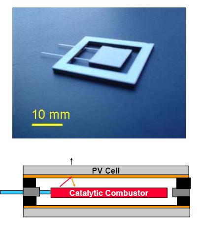
40 MIT µ-tpv T Generato r P roo jee ctt


41 Key innovations in: photonic crystals, MEMs reactors, power electronics, PV 1D photonic crystal 2D tungsten photonic crystal Low-bandgap PV cells Power electronics Si micro-fabricated reactor
42 Photonic crystals tailoring photonic- and electronic bandgaps


43 Robust, integrated catalytic micro-reactor r dee sii gnn


44 Integrated power electronics controller single chip integrated MPPT
45 Quasi-coherent thermal emission via photonic crystals Vertical-cavity resonant thermal emitter 2D PhC slab resonant thermal emission

46 Broad-band spectral control Reflectance measured simulated Wavelength (µm) Emittance flat W 2D W PhC (r=440 nm,d=315 nm) 2D W PhC (r=390 nm,d=560 nm) 2D W PhC (r=440 nm, d=560 nm) Generation Generation Narrow-band spectral control θ z ε 0 ε H ε H ε L ε H ε L ε H L 0 ε cavity ε M y

47 Vertical cavity resonant thermal emitter is highlydirectional, quasi-coherent radiation source ε 0 θ z ε H ε H ε L ε H ε L ε H L 0 ε cavity ε M y
48 Vertical cavity resonant thermal emitter: narrow-band, highly directional and Tungsten cavity mirror
49 Quasi-coherent thermal emission via photonic crystals Vertical-cavity resonant thermal emitter 2D PhC slab resonant thermal emission
50 Black/Gray- Body Physics Thermal Thermal Ref: Max Planck, Annalen der Physik, 4, 553, (1901).

51 Modes of a 2D PhC slab H z odd guided resonance z y even guided resonance mode x H z
52 Fano resonances of a 2D PhC slab z y x Ref: S. Fan and J. D. Joannopoulos, Phys. Rev. B 65, (2002).
53 Thermal emittance of a 2D PhC slab Im(ε) z y x Thermal Emittance Ref: D.Chan, I.Celanovic, J.D.Joannopoulos, and M.Soljačić, submitted for publication.

54 Dependence on angle of observation θ θ increases θ increases Thermal Emittance Thermal Emittance z y x
55 Analytical understanding of Fano resonances 2 a 2 = Q ABS Q RAD ω ω FANO Q RAD Q ABS PhC 2 2 Q ABS = ε R σε I Q ABS = Q RAD a PhC MAX = 50%
56 Rules for designing thermal emission Thermal Emittance z y x ω EMIT (θ): slab thickness Re(ε) lattice constant Γ EMIT Q RAD : size of holes Peak emission Q ABS : Im(ε) 2 2 Q ABS Q a RAD PhC = 2 ω ω FANO QRAD Q ABS 2
57 An example of thermal design z y Q RAD =370 x Q RAD =2000 Thermal
58 Quasi-coherent thermal radiation: summary and opportunities PhC s offer unprecedented opportunities for tailoring thermal emission spectra Highly anomalous thermal spectra can be obtained Even dynamical tuning of spectra is possible Research in the combined near-field and quasi-coherent PhC radiation is opening up new frontiers Possible applications include: masking thermal targets, coherent thermal sources, high-efficiency TPV generation, chemical sensing, etc.
59 MIT OpenCourseWare Direct Solar/Thermal to Electrical Energy Conversion Technologies Fall 2009 For information about citing these materials or our Terms of Use, visit:
HIGH EFFICIENCY THERMOPHOTOVOLTAIC SYSTEMS. Anubha Mathur, Enas Said Sakr, Professor Peter Bermel Purdue University
 HIGH EFFICIENCY THERMOPHOTOVOLTAIC SYSTEMS Anubha Mathur, Enas Said Sakr, Professor Peter Bermel Purdue University PRESENTATION OVERVIEW Motivation and Introduction Background Research and Methodology
Nanophotonics: solar and thermal applications
 Nanophotonics: solar and thermal applications Shanhui Fan Ginzton Laboratory and Department of Electrical Engineering Stanford University http://www.stanford.edu/~shanhui Nanophotonic Structures Photonic
Ultra High Efficiency Thermo-Photovoltaic Solar Cells Using Metallic Photonic Crystals As Intermediate Absorber and Emitter
 Ultra High Efficiency Thermo-Photovoltaic Solar Cells Using Metallic Photonic Crystals As Intermediate Absorber and Emitter A. Investigators Shanhui Fan, Associate Professor, Electrical Engineering, Stanford
Control of thermal radiation for energy applications. Shanhui Fan Ginzton Laboratory and Department of Electrical Engineering Stanford University
 Control of thermal radiation for energy applications Shanhui Fan Ginzton Laboratory and Department of Electrical Engineering Stanford University Thermal radiation: an ubiquitous aspect of nature Sun (6000K)
High temperature plasmonics: Narrowband, tunable, nearfield. thermal sources
 High temperature plasmonics: Narrowband, tunable, nearfield thermal sources Yu Guo, S. Molesky, C. Cortes and Zubin Jacob * Department of Electrical and Computer Engineering, University of Alberta, Edmonton,
PHOTOVOLTAICS Fundamentals
 PHOTOVOLTAICS Fundamentals PV FUNDAMENTALS Semiconductor basics pn junction Solar cell operation Design of silicon solar cell SEMICONDUCTOR BASICS Allowed energy bands Valence and conduction band Fermi
Electrons are shared in covalent bonds between atoms of Si. A bound electron has the lowest energy state.
 Photovoltaics Basic Steps the generation of light-generated carriers; the collection of the light-generated carriers to generate a current; the generation of a large voltage across the solar cell; and
Dielectric Meta-Reflectarray for Broadband Linear Polarization Conversion and Optical Vortex Generation
 Supporting Information Dielectric Meta-Reflectarray for Broadband Linear Polarization Conversion and Optical Vortex Generation Yuanmu Yang, Wenyi Wang, Parikshit Moitra, Ivan I. Kravchenko, Dayrl P. Briggs,
Photonic devices for quantum information processing:
 Outline Photonic devices for quantum information processing: coupling to dots, structure design and fabrication Optoelectronics Group, Cavendish Lab Outline Vuckovic s group Noda s group Outline Outline
Photonic crystals. Semi-conductor crystals for light. The smallest dielectric lossless structures to control whereto and how fast light flows
 Photonic crystals Semi-conductor crystals for light The smallest dielectric lossless structures to control whereto and how fast light flows Femius Koenderink Center for Nanophotonics AMOLF, Amsterdam f.koenderink@amolf.nl
Photonic Crystals. Introduction
 Photonic Crystals Introduction Definition Photonic crystals are new, artificialy created materials, in which refractive index is periodically modulated in a scale compared to the wavelength of operation.
Nanomaterials and their Optical Applications
 Nanomaterials and their Optical Applications Winter Semester 2012 Lecture 08 rachel.grange@uni-jena.de http://www.iap.uni-jena.de/multiphoton Outline: Photonic crystals 2 1. Photonic crystals vs electronic
Improved Thermal Emitters for Thermophotovoltaic Energy Conversion
 Improved Thermal Emitters for Thermophotovoltaic Energy Conversion The MIT Faculty has made this article openly available. Please share how this access benefits you. Your story matters. Citation As Published
High Efficiency Triple-Junction Solar Cells Employing Biomimetic Antireflective Structures
 High Efficiency Triple-Junction Solar Cells Employing Biomimetic Antireflective Structures M.Y. Chiu, C.-H. Chang, F.-Y. Chang, and Peichen Yu, Green Photonics Laboratory Department of Photonics National
Light Interaction with Small Structures
 Light Interaction with Small Structures Molecules Light scattering due to harmonically driven dipole oscillator Nanoparticles Insulators Rayleigh Scattering (blue sky) Semiconductors...Resonance absorption
Optics of complex micro structures
 Optics of complex micro structures dielectric materials λ L disordered partially ordered ordered random multiple scattering liquid crystals quasi crystals (Fibonacci) photonic crystals Assembly of photonic
Resonator Fabrication for Cavity Enhanced, Tunable Si/Ge Quantum Cascade Detectors
 Resonator Fabrication for Cavity Enhanced, Tunable Si/Ge Quantum Cascade Detectors M. Grydlik 1, P. Rauter 1, T. Fromherz 1, G. Bauer 1, L. Diehl 2, C. Falub 2, G. Dehlinger 2, H. Sigg 2, D. Grützmacher
Chapter 7. Solar Cell
 Chapter 7 Solar Cell 7.0 Introduction Solar cells are useful for both space and terrestrial application. Solar cells furnish the long duration power supply for satellites. It converts sunlight directly
LASERS. Amplifiers: Broad-band communications (avoid down-conversion)
") L- LASERS Representative applications: Amplifiers: Broad-band communications (avoid down-conversion) Oscillators: Blasting: Energy States: Hydrogen atom Frequency/distance reference, local oscillators,
L- LASERS Representative applications: Amplifiers: Broad-band communications (avoid down-conversion) Oscillators: Blasting: Energy States: Hydrogen atom Frequency/distance reference, local oscillators,
(b) Spontaneous emission. Absorption, spontaneous (random photon) emission and stimulated emission.
 Spontaneous emission. Absorption, spontaneous (random photon) emission and stimulated emission.") Lecture 10 Stimulated Emission Devices Lasers Stimulated emission and light amplification Einstein coefficients Optical fiber amplifiers Gas laser and He-Ne Laser The output spectrum of a gas laser Laser
Lecture 10 Stimulated Emission Devices Lasers Stimulated emission and light amplification Einstein coefficients Optical fiber amplifiers Gas laser and He-Ne Laser The output spectrum of a gas laser Laser
Modern optics Lasers
 Chapter 13 Phys 322 Lecture 36 Modern optics Lasers Reminder: Please complete the online course evaluation Last lecture: Review discussion (no quiz) LASER = Light Amplification by Stimulated Emission of
Thin film interference in ultra-thin layers: color coatings, tunable absorbers, and thermal emitters
 Thin film interference in ultra-thin layers: color coatings, tunable absorbers, and thermal emitters Mikhail A. Kats Harvard University School of Engineering and Applied Sciences NanoLight [Benasque] March
Nanophysics: Main trends
 Nano-opto-electronics Nanophysics: Main trends Nanomechanics Main issues Light interaction with small structures Molecules Nanoparticles (semiconductor and metallic) Microparticles Photonic crystals Nanoplasmonics
Charge Excitation. Lecture 4 9/20/2011 MIT Fundamentals of Photovoltaics 2.626/2.627 Fall 2011 Prof. Tonio Buonassisi
 Charge Excitation Lecture 4 9/20/2011 MIT Fundamentals of Photovoltaics 2.626/2.627 Fall 2011 Prof. Tonio Buonassisi 1 2.626/2.627 Roadmap You Are Here 2 2.626/2.627: Fundamentals Every photovoltaic device
Signal regeneration - optical amplifiers
 Signal regeneration - optical amplifiers In any atom or solid, the state of the electrons can change by: 1) Stimulated absorption - in the presence of a light wave, a photon is absorbed, the electron is
Stimulated Emission Devices: LASERS
 Stimulated Emission Devices: LASERS 1. Stimulated Emission and Photon Amplification E 2 E 2 E 2 hυ hυ hυ In hυ Out hυ E 1 E 1 E 1 (a) Absorption (b) Spontaneous emission (c) Stimulated emission The Principle
EV Group. Engineered Substrates for future compound semiconductor devices
 EV Group Engineered Substrates for future compound semiconductor devices Engineered Substrates HB-LED: Engineered growth substrates GaN / GaP layer transfer Mobility enhancement solutions: III-Vs to silicon
Thermal Emission in the Near Field from Polar Semiconductors and the Prospects for Energy Conversion
 Thermal Emission in the Near Field from Polar Semiconductors and the Prospects for Energy Conversion R.J. Trew, K.W. Kim, V. Sokolov, and B.D Kong Electrical and Computer Engineering North Carolina State
High Power Diode Lasers
 Lecture 10/1 High Power Diode Lasers Low Power Lasers (below tenth of mw) - Laser as a telecom transmitter; - Laser as a spectroscopic sensor; - Laser as a medical diagnostic tool; - Laser as a write-read
3.003 Principles of Engineering Practice
 3.003 Principles of Engineering Practice One Month Review Solar Cells The Sun Semiconductors pn junctions Electricity 1 Engineering Practice 1. Problem Definition 2. Constraints 3. Options 4. Analysis
Modeling of an efficient Thermo-Photovoltaic (TPV) cell as a power source for space application
 cell as a power source for space application") Modeling of an efficient Thermo-Photovoltaic (TPV) cell as a power source for space application Khomdram Jolson Singh Dept. of ECE. Manipur I nst it ut e of T echnology Imphal-795004 (India) jolly4u2@rediffmail.com
Modeling of an efficient Thermo-Photovoltaic (TPV) cell as a power source for space application Khomdram Jolson Singh Dept. of ECE. Manipur I nst it ut e of T echnology Imphal-795004 (India) jolly4u2@rediffmail.com
Supporting information. Unidirectional Doubly Enhanced MoS 2 Emission via
 Supporting information Unidirectional Doubly Enhanced MoS 2 Emission via Photonic Fano Resonances Xingwang Zhang, Shinhyuk Choi, Dake Wang, Carl H. Naylor, A. T. Charlie Johnson, and Ertugrul Cubukcu,,*
arxiv: v2 [physics.optics] 23 May 2016
![arxiv: v2 [physics.optics] 23 May 2016](/thumbs/77/75337351.jpg "arxiv: v2 [physics.optics] 23 May 2016") Optimized aperiodic broadband thermal emitters for use as light bulb filaments arxiv:1605.00731v2 [physics.optics] 23 May 2016 1. Introduction Christopher H. Granier, 1 Simón G. Lorenzo, 1,2, Chenglong
Optimized aperiodic broadband thermal emitters for use as light bulb filaments arxiv:1605.00731v2 [physics.optics] 23 May 2016 1. Introduction Christopher H. Granier, 1 Simón G. Lorenzo, 1,2, Chenglong
Lasers. Stimulated Emission Lasers: Trapping Photons Terahertz Lasers Course Overview
 Lasers Stimulated Emission Lasers: Trapping Photons Terahertz Lasers Course Overview 1 P-N Junctions and LEDs Terminal Pins Emitted Light Beams Diode Transparent Plastic Case High energy electrons (n-type)
Interested in exploring science or math teaching as a career?
 Interested in exploring science or math teaching as a career? Start with Step 1: EDUC 2020 (1 credit) Real experience teaching real kids! No commitment to continue with education courses Registration priority
Research on the Wide-angle and Broadband 2D Photonic Crystal Polarization Splitter
 Progress In Electromagnetics Research Symposium 2005, Hangzhou, China, August 22-26 551 Research on the Wide-angle and Broadband 2D Photonic Crystal Polarization Splitter Y. Y. Li, P. F. Gu, M. Y. Li,
Selective emitters design and optimization for thermophotovoltaic applications
 Selective emitters design and optimization for thermophotovoltaic applications E. Nefzaoui, J. Drevillon, and K. Joulain Institut Pprime, CNRS-Université de Poitiers-ENSMA, Département Fluides, Thermique,
Photovoltaic Energy Conversion. Frank Zimmermann
 Photovoltaic Energy Conversion Frank Zimmermann Solar Electricity Generation Consumes no fuel No pollution No greenhouse gases No moving parts, little or no maintenance Sunlight is plentiful & inexhaustible
ECE 695 Numerical Simulations Lecture 35: Solar Hybrid Energy Conversion Systems. Prof. Peter Bermel April 12, 2017
 ECE 695 Numerical Simulations Lecture 35: Solar Hybrid Energy Conversion Systems Prof. Peter Bermel April 12, 2017 Ideal Selective Solar Absorber Efficiency Limits Ideal cut-off wavelength for a selective
Appendix. Photonic crystal lasers: future integrated devices
 91 Appendix Photonic crystal lasers: future integrated devices 5.1 Introduction The technology of photonic crystals has produced a large variety of new devices. However, photonic crystals have not been
Understanding Nanoplasmonics. Greg Sun University of Massachusetts Boston
 Understanding Nanoplasmonics Greg Sun University of Massachusetts Boston Nanoplasmonics Space 100pm 1nm 10nm 100nm 1μm 10μm 100μm 1ns 100ps 10ps Photonics 1ps 100fs 10fs 1fs Time Surface Plasmons Surface
Electromagnetic Metamaterials
 Photonic Bandgap and Electromagnetic Metamaterials Andrew Kirk andrew.kirk@mcgill.ca ca Department of Electrical and Computer Engineering McGill Institute for Advanced Materials A Kirk 11/24/2008 Photonic
2.626 Fundamentals of Photovoltaics
 MIT OpenCourseWare http://ocw.mit.edu 2.626 Fundamentals of Photovoltaics Fall 2008 For information about citing these materials or our Terms of Use, visit: http://ocw.mit.edu/terms. Quiz #1 Review: Fundamentals
Nanoscale Heat Transfer and Information Technology
 Response to K.E. Goodson Nanoscale Heat Transfer and Information Technology Gang Chen Mechanical Engineering Department Massachusetts Institute of Technology Cambridge, MA 02139 Rohsenow Symposium on Future
Demonstration of Near-Infrared Negative-Index Materials
 Demonstration of Near-Infrared Negative-Index Materials Shuang Zhang 1, Wenjun Fan 1, N. C. Panoiu 2, K. J. Malloy 1, R. M. Osgood 2 and S. R. J. Brueck 2 1. Center for High Technology Materials and Department
The Shockley-Queisser Limit. Jake Friedlein 7 Dec. 2012
 The Shockley-Queisser Limit Jake Friedlein 7 Dec. 2012 1 Outline A. Loss factors 1. Bandgap energy 2. Geometric factor 3. Recombination of electrons and holes B. Overall efficiency C. Optimum bandgap 2
Spectra from transitions in atoms and lighting
 Spectra from transitions in atoms and lighting Safety: This experiment uses a Mercury Light source and a laser. Mercury light source emits Ultraviolet light. You should always have the ground glass shield
Development of spectrally selective infrared emitter for thermophotovoltaic power generation
 Development of spectrally selective infrared emitter for thermophotovoltaic power generation 波長選択機能を有する熱光起電力発電用赤外線源の開発 Motofumi Suzuki, Department of Micro Engineering, Kyoto University 1. Introduction
InAs/GaSb Mid-Wave Cascaded Superlattice Light Emitting Diodes
 InAs/GaSb Mid-Wave Cascaded Superlattice Light Emitting Diodes John Prineas Department of Physics and Astronomy, University of Iowa May 3, 206 Collaborator: Thomas Boggess Grad Students: Yigit Aytak Cassandra
Micro- and Nano-Technology... for Optics
 Micro- and Nano-Technology...... for Optics U.D. Zeitner Fraunhofer Institut für Angewandte Optik und Feinmechanik Jena Today: 1. Introduction E. Bernhard Kley Institute of Applied Physics Friedrich-Schiller
Quantum Dot Technology for Low-Cost Space Power Generation for Smallsats
 SSC06-VI- Quantum Dot Technology for Low-Cost Space Power Generation for Smallsats Theodore G. DR Technologies, Inc. 7740 Kenamar Court, San Diego, CA 92020 (858)677-230 tstern@drtechnologies.com The provision
One dimensional TiO 2 /SiO 2 photonic crystal filter for thermophotovoltaic applications
 Mbakop et al. Journal of the European Optical Society-Rapid Publications (2016) 12:23 DOI 10.1186/s41476-016-0026-4 Journal of the European Optical Society-Rapid Publications RESEARCH Open Access One dimensional
Polarization control and sensing with two-dimensional coupled photonic crystal microcavity arrays. Hatice Altug * and Jelena Vučković
 Polarization control and sensing with two-dimensional coupled photonic crystal microcavity arrays Hatice Altug * and Jelena Vučković Edward L. Ginzton Laboratory, Stanford University, Stanford, CA 94305-4088
ENERGY NANOTECHNOLOGY --- A Few Examples
 ENERGY NANOTECHNOLOGY --- A Few Examples Gang Chen Nanoengineering Group Rohsenow Heat and Mass Transfer Laboratory Massachusetts Institute of Technology Cambridge, MA 02139 Email: gchen2@mit.edu http://web.mit.edu/nanoengineering
Fabrication Technology, Part I
 EEL5225: Principles of MEMS Transducers (Fall 2004) Fabrication Technology, Part I Agenda: Microfabrication Overview Basic semiconductor devices Materials Key processes Oxidation Thin-film Deposition Reading:
Photonic Crystals: Periodic Surprises in Electromagnetism. You can leave home without them. Complete Band Gaps: Steven G.
 Photonic Crystals: Periodic Surprises in lectromagnetism Steven G. ohnson MIT Complete Band Gaps: You can leave home without them. How else can we confine light? Total Internal Reflection n o n i > n o
Laser Basics. What happens when light (or photon) interact with a matter? Assume photon energy is compatible with energy transition levels.
 interact with a matter? Assume photon energy is compatible with energy transition levels.") What happens when light (or photon) interact with a matter? Assume photon energy is compatible with energy transition levels. Electron energy levels in an hydrogen atom n=5 n=4 - + n=3 n=2 13.6 = [ev]
What happens when light (or photon) interact with a matter? Assume photon energy is compatible with energy transition levels. Electron energy levels in an hydrogen atom n=5 n=4 - + n=3 n=2 13.6 = [ev]
Chemistry Instrumental Analysis Lecture 5. Chem 4631
 Chemistry 4631 Instrumental Analysis Lecture 5 Light Amplification by Stimulated Emission of Radiation High Intensities Narrow Bandwidths Coherent Outputs Applications CD/DVD Readers Fiber Optics Spectroscopy
Angular and polarization properties of a photonic crystal slab mirror
 Angular and polarization properties of a photonic crystal slab mirror Virginie Lousse 1,2, Wonjoo Suh 1, Onur Kilic 1, Sora Kim 1, Olav Solgaard 1, and Shanhui Fan 1 1 Department of Electrical Engineering,
Analysis of Photonic Band Structure in 1-D Photonic Crystal using PWE and FDTD Method
 P P IJISET - International Journal of Innovative Science, Engineering & Technology, Vol. Issue 8, August 05. Analysis of Photonic Band Structure in -D Photonic Crystal using PWE and FDTD Method Pooja ChhokerP
Photon Extraction: the key physics for approaching solar cell efficiency limits
 Photon Extraction: the key physics for approaching solar cell efficiency limits Owen Miller*: Post-doc, MIT Math Eli Yablonovitch: UC Berkeley, LBNL Slides/Codes/Relevant Papers: math.mit.edu/~odmiller/publications
Optimization of enhanced absorption in 3D-woodpile metallic photonic crystals
 Optimization of enhanced absorption in 3D-woodpile metallic photonic crystals Md Muntasir Hossain 1, Gengyan Chen 2, Baohua Jia 1, Xue-Hua Wang 2 and Min Gu 1,* 1 Centre for Micro-Photonics and CUDOS,
Supplementary Information for Negative refraction in semiconductor metamaterials
 Supplementary Information for Negative refraction in semiconductor metamaterials A.J. Hoffman *, L. Alekseyev, S.S. Howard, K.J. Franz, D. Wasserman, V.A. Poldolskiy, E.E. Narimanov, D.L. Sivco, and C.
PRESENTED BY: PROF. S. Y. MENSAH F.A.A.S; F.G.A.A.S UNIVERSITY OF CAPE COAST, GHANA.
 SOLAR CELL AND ITS APPLICATION PRESENTED BY: PROF. S. Y. MENSAH F.A.A.S; F.G.A.A.S UNIVERSITY OF CAPE COAST, GHANA. OUTLINE OF THE PRESENTATION Objective of the work. A brief introduction to Solar Cell
Homework 1. Property LASER Incandescent Bulb
 Homework 1 Solution: a) LASER light is spectrally pure, single wavelength, and they are coherent, i.e. all the photons are in phase. As a result, the beam of a laser light tends to stay as beam, and not
Comparison of Ge, InGaAs p-n junction solar cell
 ournal of Physics: Conference Series PAPER OPEN ACCESS Comparison of Ge, InGaAs p-n junction solar cell To cite this article: M. Korun and T. S. Navruz 16. Phys.: Conf. Ser. 77 135 View the article online
Photo-Thermal Engineering for Clean Energy and Water Applications
 Photo-Thermal Engineering for Clean Energy and Water Applications Ravi Prasher Associate Lab Director Energy Technology Area Lawrence Berkeley National Lab Adjunct Professor Department of Mechanical Engineering
PHYS 219 General Physics: Electricity, Light and Modern Physics
 PHYS 219 General Physics: Electricity, Light and Modern Physics Final exam is scheduled on Thursday May 2 @ 8 10 AM In Physics 112 It will cover five Chapters 25, 27, 28, 29, and 30. Review lecture notes,
Problem One Answer the following questions concerning fundamental radiative heat transfer. (2 points each) Part Question Your Answer
 Part Question Your Answer") Problem One Answer the following questions concerning fundamental radiative heat transfer. ( points each) Part Question Your Answer A Do all forms of matter emit radiation? Yes B Does the transport of
Problem One Answer the following questions concerning fundamental radiative heat transfer. ( points each) Part Question Your Answer A Do all forms of matter emit radiation? Yes B Does the transport of
Lecture 3: Optical Properties of Insulators, Semiconductors, and Metals. 5 nm
 Metals Lecture 3: Optical Properties of Insulators, Semiconductors, and Metals 5 nm Course Info Next Week (Sept. 5 and 7) no classes First H/W is due Sept. 1 The Previous Lecture Origin frequency dependence
PLASMONICS/METAMATERIALS
 PLASMONICS/METAMATERIALS Interconnects Optical processing of data Subwavelength confinement Electrodes are in place Coupling to other on-chip devices Combination of guiding, detection, modulation, sensing
Toward a 1D Device Model Part 1: Device Fundamentals
 Toward a 1D Device Model Part 1: Device Fundamentals Lecture 7 9/29/2011 MIT Fundamentals of Photovoltaics 2.626/2.627 Fall 2011 Prof. Tonio Buonassisi 1 Learning Objectives: Toward a 1D Device Model 1.
Chapter 24 Photonics Question 1 Question 2 Question 3 Question 4 Question 5
 Chapter 24 Photonics Data throughout this chapter: e = 1.6 10 19 C; h = 6.63 10 34 Js (or 4.14 10 15 ev s); m e = 9.1 10 31 kg; c = 3.0 10 8 m s 1 Question 1 Visible light has a range of photons with wavelengths
Theoretical Approach to Simulate Efficient Selective Solar Absorbers With Micro or Nano Structured Arrays. 1. Introduction
 Materials Research. 218; 21(): e217126 DOI: http://dx.doi.org/1.159/198-57-mr-217-126 Theoretical Approach to Simulate Efficient Selective Solar Absorbers With Micro or Nano Structured Arrays Jhong-sian
arxiv: v1 [physics.optics] 12 Jun 2014
![arxiv: v1 [physics.optics] 12 Jun 2014](/thumbs/94/121282336.jpg "arxiv: v1 [physics.optics] 12 Jun 2014") Intermediate Mirrors to Reach Theoretical Efficiency Limits of Multi-Bandgap Solar Cells arxiv:1406.3126v1 [physics.optics] 12 Jun 2014 Abstract Vidya Ganapati, Chi-Sing Ho, Eli Yablonovitch University
Intermediate Mirrors to Reach Theoretical Efficiency Limits of Multi-Bandgap Solar Cells arxiv:1406.3126v1 [physics.optics] 12 Jun 2014 Abstract Vidya Ganapati, Chi-Sing Ho, Eli Yablonovitch University
Emission pattern control and polarized light emission through patterned graded-refractiveindex coatings on GaInN light-emitting diodes
 Emission pattern control and polarized light emission through patterned graded-refractiveindex coatings on GaInN light-emitting diodes Ming Ma, 1 Ahmed N. Noemaun, 2 Jaehee Cho, 2,* E. Fred Schubert, 2
Fall 2014 Nobby Kobayashi (Based on the notes by E.D.H Green and E.L Allen, SJSU) 1.0 Learning Objectives
 1.0 Learning Objectives") University of California at Santa Cruz Electrical Engineering Department EE-145L: Properties of Materials Laboratory Lab 7: Optical Absorption, Photoluminescence Fall 2014 Nobby Kobayashi (Based on the
University of California at Santa Cruz Electrical Engineering Department EE-145L: Properties of Materials Laboratory Lab 7: Optical Absorption, Photoluminescence Fall 2014 Nobby Kobayashi (Based on the
Supplementary Figure 1: Experimental measurement of polarization-dependent absorption properties in all-fibre graphene devices. a.
 Supplementary Figure 1: Experimental measurement of polarization-dependent absorption properties in all-fibre graphene devices. a. Schematic of experimental set-up including an amplified spontaneous emission
Introduction to Photonic Crystals
 1 Introduction to Photonic Crystals Summary. Chapter 1 gives a brief introduction into the basics of photonic crystals which are a special class of optical media with periodic modulation of permittivity.
Third generation solar cells - How to use all the pretty colours?
 Third generation solar cells - How to use all the pretty colours? Erik Stensrud Marstein Department for Solar Energy Overview The trouble with conventional solar cells Third generation solar cell concepts
Seminars in Nanosystems - I
 Seminars in Nanosystems - I Winter Semester 2011/2012 Dr. Emanuela Margapoti Emanuela.Margapoti@wsi.tum.de Dr. Gregor Koblmüller Gregor.Koblmueller@wsi.tum.de Seminar Room at ZNN 1 floor Topics of the
Photonic Crystal Nanocavities for Efficient Light Confinement and Emission
 Journal of the Korean Physical Society, Vol. 42, No., February 2003, pp. 768 773 Photonic Crystal Nanocavities for Efficient Light Confinement and Emission Axel Scherer, T. Yoshie, M. Lončar, J. Vučković
Two-dimensional lattice
 Two-dimensional lattice a 1 *, k x k x =0,k y =0 X M a 2, y Γ X a 2 *, k y a 1, x Reciprocal lattice Γ k x = 0.5 a 1 *, k y =0 k x = 0, k y = 0.5 a 2 * k x =0.5a 1 *, k y =0.5a 2 * X X M k x = 0.25 a 1
Plasmonics. The long wavelength of light ( μm) creates a problem for extending optoelectronics into the nanometer regime.
 creates a problem for extending optoelectronics into the nanometer regime.") Plasmonics The long wavelength of light ( μm) creates a problem for extending optoelectronics into the nanometer regime. A possible way out is the conversion of light into plasmons. They have much shorter
Plasmonics The long wavelength of light ( μm) creates a problem for extending optoelectronics into the nanometer regime. A possible way out is the conversion of light into plasmons. They have much shorter
Fundamental Limitations of Solar Cells
 2018 Lecture 2 Fundamental Limitations of Solar Cells Dr Kieran Cheetham MPhys (hons) CPhys MInstP MIET L3 Key Question Why can't a solar cell have a 100% efficiency? (Or even close to 100%?) Can you answer
TUNABLE MULTI-CHANNEL FILTERING USING 1-D PHOTONIC QUANTUM WELL STRUCTURES
 Progress In Electromagnetics Research Letters, Vol. 27, 43 51, 2011 TUNABLE MULTI-CHANNEL FILTERING USING 1-D PHOTONIC QUANTUM WELL STRUCTURES B. Suthar * and A. Bhargava Nanophysics Laboratory, Department
Acoustics and Fourier Transform
 AFT Acoustics and Fourier Transform 1. A Hamming filter is used to compute FFT (Fast Fourier Transform) plots in the AFT experiment. What is the reason for using such a filter? 2. Briefly describe what
Magneto-Optical Cavity-Type Resonators as Controllable Narrow-Band Sources of Infrared Radiation
 American Journal of Modern Physics and Application 8; 5(4): 77-8 http://www.openscienceonline.com/journal/ajmpa Magneto-Optical Cavity-Type Resonators as Controllable Narrow-Band Sources of Infrared Radiation
Progress In Electromagnetics Research Letters, Vol. 42, 13 22, 2013
 Progress In Electromagnetics Research Letters, Vol. 42, 3 22, 23 OMNIDIRECTIONAL REFLECTION EXTENSION IN A ONE-DIMENSIONAL SUPERCONDUCTING-DIELECTRIC BINARY GRADED PHOTONIC CRYSTAL WITH GRADED GEOMETRIC
Ge Quantum Well Modulators on Si. D. A. B. Miller, R. K. Schaevitz, J. E. Roth, Shen Ren, and Onur Fidaner
 10.1149/1.2986844 The Electrochemical Society Ge Quantum Well Modulators on Si D. A. B. Miller, R. K. Schaevitz, J. E. Roth, Shen Ren, and Onur Fidaner Ginzton Laboratory, 450 Via Palou, Stanford CA 94305-4088,
OPTICAL PROPERTIES of Nanomaterials
 OPTICAL PROPERTIES of Nanomaterials Advanced Reading Optical Properties and Spectroscopy of Nanomaterials Jin Zhong Zhang World Scientific, Singapore, 2009. Optical Properties Many of the optical properties
A Multipass Optics for Quantum-Well-Pumped Semiconductor Disk Lasers
 Multipass-Pumped Semiconductor Disk Lasers 37 A Multipass Optics for Quantum-Well-Pumped Semiconductor Disk Lasers Markus Polanik The pump absorption of quantum-well-pumped semiconductor disk lasers can
OPAC 101 Introduction to Optics
 OPAC 101 Introduction to Optics Topic 2 Light Sources Department of http://www1.gantep.edu.tr/~bingul/opac101 Optical & Acustical Engineering Gaziantep University Sep 2017 Sayfa 1 Light Sources: maybe
Preview from Notesale.co.uk Page 1 of 38
 F UNDAMENTALS OF PHOTONICS Module 1.1 Nature and Properties of Light Linda J. Vandergriff Director of Photonics System Engineering Science Applications International Corporation McLean, Virginia Light
EE 5344 Introduction to MEMS CHAPTER 5 Radiation Sensors
 EE 5344 Introduction to MEMS CHAPTER 5 Radiation Sensors 5. Radiation Microsensors Radiation µ-sensors convert incident radiant signals into standard electrical out put signals. Radiant Signals Classification
Photonic Band Gap Crystals. Srivatsan Balasubramanian
 Photonic Band Gap Crystals Srivatsan Balasubramanian Summary Physics of photonic bandgap crystals. Photonic Crystals Classification. Fabrication. Applications. Protoype photonic band gap devices. Current
1. Reminder: E-Dynamics in homogenous media and at interfaces
 0. Introduction 1. Reminder: E-Dynamics in homogenous media and at interfaces 2. Photonic Crystals 2.1 Introduction 2.2 1D Photonic Crystals 2.3 2D and 3D Photonic Crystals 2.4 Numerical Methods 2.5 Fabrication
Nanostrukturphysik (Nanostructure Physics)
") Nanostrukturphysik (Nanostructure Physics) Prof. Yong Lei & Dr. Yang Xu Fachgebiet 3D-Nanostrukturierung, Institut für Physik Contact: yong.lei@tu-ilmenau.de; yang.xu@tu-ilmenau.de Office: Unterpoerlitzer
Nanostrukturphysik (Nanostructure Physics) Prof. Yong Lei & Dr. Yang Xu Fachgebiet 3D-Nanostrukturierung, Institut für Physik Contact: yong.lei@tu-ilmenau.de; yang.xu@tu-ilmenau.de Office: Unterpoerlitzer
A World of Color. Session 2. OLLI at Illinois Spring D. H. Tracy
 A World of Color Session 2 OLLI at Illinois Spring 2018 D. H. Tracy Course Outline 1. Overview, History and Spectra 2. Nature and Sources of Light 3. Eyes and Color Vision 4. Origins of Colors of Things