High Efficiency Triple-Junction Solar Cells Employing Biomimetic Antireflective Structures
|
|
|
- Lillian French
- 5 years ago
- Views:
Transcription

1 High Efficiency Triple-Junction Solar Cells Employing Biomimetic Antireflective Structures M.Y. Chiu, C.-H. Chang, F.-Y. Chang, and Peichen Yu, Green Photonics Laboratory Department of Photonics National Chiao-Tung University, Hsinchu, Taiwan

2 Outline Introduction Biomimetics Moth-eye principle Device Fabrication Process Polystyrene nanosphere lithography Optical and Photovoltaic Characteristics Reflectance Engineering via RCWA* Summary *RCWA: rigorous coupled-wave analysis ERATO Symposium, Tohoku Univ. Japan 2011/2/16 2/16


3 Biomimetics Self-cleaning abilities of a lotus leave: ERATO Symposium, Tohoku Univ. Japan 2011/2/16 3/16

4 Biomimetics Colors of butterfly wings: Man-made polymer photonic crystals ERATO Symposium, Tohoku Univ. Japan 2011/2/16 4/16


5 Biomimetic Antireflective Structures The moth-eye principle : broadband and omni-directional AR Si Polymer ERATO Symposium, Tohoku Univ. Japan 2011/2/16 5/16

6 Moth-eye principle Sub-wavelength structure (SWS) λ n a i r n air Graded-index semiconductor n s n eff ERATO Symposium, Tohoku Univ. Japan 2011/2/16 6/16
7 air Introduction Graded refractive index profile n air n Multi-layer ARC: Material selection for different refractive indices Thermal constant mismatch that change mechanical and optical properties semiconductor n s Biomimetic ARC: Single layer SWS Mechanically and optically robust and durable Profile control possible *ARC: antireflective coating ERATO Symposium, Tohoku Univ. Japan 2011/2/16 7/16
8 Triple-junction solar cell I ng ap G aa s Ge Power conversion Efficiency ~40% ERATO Symposium, Tohoku Univ. Japan 2011/2/16 8/16
9 Triple-junction solar cell with SWS Ga 0.5 In 0.5 P/GaAs/Ge Triple-junction solar cell Broadband absorption (300nm ~1800nm) Very thin thickness (~ a few micrometers) InGaP GaAs λ Ge Surface Recombination =>SWS fabricated on SiNx passivation layer Current Matching => Reflectance engineering ERATO Symposium, Tohoku Univ. Japan 2011/2/16 9/16

 sphere Substrate 4 wafer 10")
10 Polystyrene Nanosphere Lithography Requirements for substrate Hydrophilic surface Homogeneous chemical property Flat and clean surface Spin Coating: 1.Scan speed 2.PS solution concentration Poly Styrene (PS) sphere Substrate 4 wafer 10 μm ERATO Symposium, Tohoku Univ. Japan 2011/2/16 10/16
 P o l y s t y r e n e")
 T J w a f e r T J w a f e r T J w a f e r")

11 Profile Control via RIE Sacrificial mask for reactive ion etching (RIE) P o l y s t y r e n e SiN x (n~1.8) T J w a f e r T J w a f e r T J w a f e r 1-step etching 2-step etching μ m nm 200 nm ~100 nm-thick SiN x was kept for passivation ERATO Symposium, Tohoku Univ. Japan 2011/2/16 11 /16
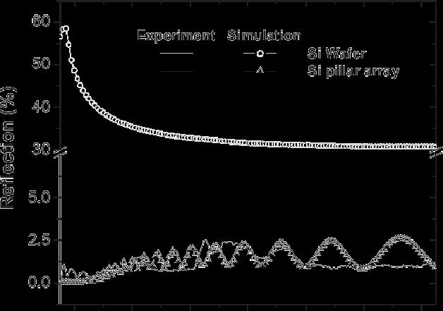
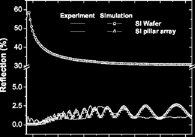
12 Optical Characterization Reflectance spectra (measured by an integrating sphere) Reflectiveity (%) SL-ARC SWS AM1.5D W a v e l e n g t h ( n m ) Irradiance (Wm -2 nm - 1 ) SWS shows a much flatter spectrum, particularly in UV and IR. Reflectance of SWS can be further improved by choosing a passivation material with a higher refractive index than SiNx, ~1.8. SWS designed to enhance the spectral response of the current limited junction ERATO Symposium, Tohoku Univ. Japan 2011/2/16 12/16


13 Device Fabrication Flow 3J wafer pattern ohmic GaAs 1um SiN x deposition top cell: Ga 0. 5 In 0. 5 P middle cell : GaAs front contact cap GaAs metal evaporation RIE etching for SWS spin on PS spheres bo t to m c el l : G e rear contact ERATO Symposium, Tohoku Univ. Japan 2011/2/16 13/16
 1 4 1 2 1 0 8 6 4 2 S W S S L - A R C no ARC 0 0.0 0.5 1.0 1.")
 9.36 11.37 11.62 F F( % ) 84.98 86.42 86.")

14 Device Characterization Current-Voltage measurement No ARC SL-ARC SWS Current Density (ma/cm 2 ) S W S S L - A R C no ARC V o l t a g e ( V ) AR condition w/o ARC SL ARC SWS V o c ( V ) Jsc (ma/cm 2 ) F F( % ) Efficiency (%) Jsc is increased by 24.2% and 2.2%, compared to those without ARC and with SLARC, respectively. ERATO Symposium, Tohoku Univ. Japan 2011/2/16 14/16
15 Rigorous Coupled Wave Analysis Modeling parameters SWS AR passivation Window layer Top cell 7x7 hexagonal SiN x parabola array Periodicity~600 nm Height ~ 900nm SiN x 100 nm 50% AlInP 50 nm 50%GaInP 500 nm 1. A l 0.5 In 0.5 P and Ga 0.5 In 0.5 P n,k mismatch. 2. Only top cell is included. ERATO Symposium, Tohoku Univ. Japan 2011/2/16 15/16

16 Summary We have successfully fabricated SiN x -based SWS for a Ga 0.5 In 0.5 P/GaAs/Ge triple-junction solar cell utilizing the polystyrene nanosphere lithography. PCE and Jsc of triple-junction solar cell were enhanced due to the absorption improvement of the GaAs mid-cell. The angular response of photocurrent nearly follows the cosine law and demonstrates the omnidirectionality of SWS. An RCWA approach enables the reflectance engineering for Jsc optimization of tandem cells with the SWS. ERATO Symposium, Tohoku Univ. Japan 2011/2/16 16/16
17 Thanks for your attention!! ERATO Symposium, Tohoku Univ. Japan at NCTU 17/16
Chapter 7. Solar Cell
 Chapter 7 Solar Cell 7.0 Introduction Solar cells are useful for both space and terrestrial application. Solar cells furnish the long duration power supply for satellites. It converts sunlight directly
Supplementary Information. Light Manipulation for Organic Optoelectronics Using Bio-inspired Moth's Eye. Nanostructures
 Supplementary Information Light Manipulation for Organic Optoelectronics Using Bio-inspired Moth's Eye Nanostructures Lei Zhou, Qing-Dong Ou, Jing-De Chen, Su Shen, Jian-Xin Tang,* Yan-Qing Li,* and Shuit-Tong
(Co-PIs-Mark Brongersma, Yi Cui, Shanhui Fan) Stanford University. GCEP Research Symposium 2013 Stanford, CA October 9, 2013
 Stanford University. GCEP Research Symposium 2013 Stanford, CA October 9, 2013") High-efficiency thin film nano-structured multi-junction solar James S. cells Harris (PI) (Co-PIs-Mark Brongersma, Yi Cui, Shanhui Fan) Stanford University GCEP Research Symposium 2013 Stanford, CA October
High-efficiency thin film nano-structured multi-junction solar James S. cells Harris (PI) (Co-PIs-Mark Brongersma, Yi Cui, Shanhui Fan) Stanford University GCEP Research Symposium 2013 Stanford, CA October
PHOTOVOLTAICS Fundamentals
 PHOTOVOLTAICS Fundamentals PV FUNDAMENTALS Semiconductor basics pn junction Solar cell operation Design of silicon solar cell SEMICONDUCTOR BASICS Allowed energy bands Valence and conduction band Fermi
Advanced Texturing of Si Nanostructures on Low Lifetime Si Wafer
 Advanced Texturing of Si Nanostructures on Low Lifetime Si Wafer SUHAILA SEPEAI, A.W.AZHARI, SALEEM H.ZAIDI, K.SOPIAN Solar Energy Research Institute (SERI), Universiti Kebangsaan Malaysia (UKM), 43600
Solar Energy Materials & Solar Cells
 Solar Energy Materials & Solar Cells 95 (211) 261 2615 Contents lists available at ScienceDirect Solar Energy Materials & Solar Cells journal homepage: www.elsevier.com/locate/solmat Angle-resolved characteristics
High resolution THz scanning for optimization of dielectric layer opening process on doped Si surfaces
 High resolution THz scanning for optimization of dielectric layer opening process on doped Si surfaces P. Spinelli 1, F.J.K. Danzl 1, D. Deligiannis 1,2, N. Guillevin 1, A.R. Burgers 1, S. Sawallich 3,
Nanostrukturphysik (Nanostructure Physics)
") Nanostrukturphysik (Nanostructure Physics) Prof. Yong Lei & Dr. Yang Xu Fachgebiet 3D-Nanostrukturierung, Institut für Physik Contact: yong.lei@tu-ilmenau.de; yang.xu@tu-ilmenau.de Office: Unterpoerlitzer
Nanostrukturphysik (Nanostructure Physics) Prof. Yong Lei & Dr. Yang Xu Fachgebiet 3D-Nanostrukturierung, Institut für Physik Contact: yong.lei@tu-ilmenau.de; yang.xu@tu-ilmenau.de Office: Unterpoerlitzer
Nanosphere Lithography
 Nanosphere Lithography Derec Ciafre 1, Lingyun Miao 2, and Keita Oka 1 1 Institute of Optics / 2 ECE Dept. University of Rochester Abstract Nanosphere Lithography is quickly emerging as an efficient, low
Multiple-Patterning Nanosphere Lithography for Fabricating Periodic Three-Dimensional Hierarchical Nanostructures
 Supporting Information Multiple-Patterning Nanosphere Lithography for Fabricating Periodic Three-Dimensional Hierarchical Nanostructures Xiaobin Xu, 1,2 Qing Yang, 1,2 Natcha Wattanatorn, 1,2 Chuanzhen
Nanophotonics: solar and thermal applications
 Nanophotonics: solar and thermal applications Shanhui Fan Ginzton Laboratory and Department of Electrical Engineering Stanford University http://www.stanford.edu/~shanhui Nanophotonic Structures Photonic
Analysis of Energy Production of Spectrolab Multijunction Solar Cells in Field Conditions
 Analysis of Energy Production of Spectrolab Multijunction Solar Cells in Field Conditions R. K. Jones, R. R. King, C. M. Fetzer, J. H. Ermer, K. M. Edmondson, P. Hebert Spectrolab, Inc., Sylmar, California,,
REFRACTORY METAL OXIDES: FABRICATION OF NANOSTRUCTURES, PROPERTIES AND APPLICATIONS
 REFRACTORY METAL OXIDES: FABRICATION OF NANOSTRUCTURES, PROPERTIES AND APPLICATIONS S.K. Lazarouk, D.A. Sasinovich BELARUSIAN STATE UNIVERSITY OF INFORMATICS AND RADIOELECTRONICS Outline: -- experimental
Demonstration of Near-Infrared Negative-Index Materials
 Demonstration of Near-Infrared Negative-Index Materials Shuang Zhang 1, Wenjun Fan 1, N. C. Panoiu 2, K. J. Malloy 1, R. M. Osgood 2 and S. R. J. Brueck 2 1. Center for High Technology Materials and Department
Graded S i N x /S i O x N y Layers as Antireflective Coatings for Solar Cells Based on GaAs and Silicon Crystalline
 Science Research 2016; 4(1): 21-25 Published online February 25, 2016 (http://www.sciencepublishinggroup.com/j/sr) doi: 10.11648/j.sr.20160401.14 ISSN: 2329-0935 (Print); ISSN: 2329-0927 (Online) Graded
The Opto-Electronic Physics That Just Broke the Efficiency Record in Solar Cells
 The Opto-Electronic Physics That Just Broke the Efficiency Record in Solar Cells Solar Energy Mini-Series Jen-Hsun Huang Engineering Center Stanford, California Sept. 26, 2011 Owen D. Miller & Eli Yablonovitch
OPTI510R: Photonics. Khanh Kieu College of Optical Sciences, University of Arizona Meinel building R.626
 OPTI510R: Photonics Khanh Kieu College of Optical Sciences, University of Arizona kkieu@optics.arizona.edu Meinel building R.626 Announcements HW#3 is assigned due Feb. 20 st Mid-term exam Feb 27, 2PM
Analyze the effect of window layer (AlAs) for increasing the efficiency of GaAs based solar cell
 for increasing the efficiency of GaAs based solar cell") American Journal of Engineering Research (AJER) e-issn: 2320-0847 p-issn : 2320-0936 Volume-4, Issue-7, pp-304-315 www.ajer.org Research Paper Open Access Analyze the effect of window layer (AlAs) for
American Journal of Engineering Research (AJER) e-issn: 2320-0847 p-issn : 2320-0936 Volume-4, Issue-7, pp-304-315 www.ajer.org Research Paper Open Access Analyze the effect of window layer (AlAs) for
Modeling III-V Semiconductor Solar Cells
 Modeling III-V Semiconductor Solar Cells Ideal limits to real device modeling A. W. Walker Fraunhofer Institute for Solar Energy Systems ISE PROMIS Workshop Cadiz, Spain May 18-20 th, 2016 www.ise.fraunhofer.de
Supporting Information. Monolithic perovskite-homojunction silicon tandem solar cell with over 22% efficiency
 Electronic Supplementary Material (ESI) for Energy & Environmental Science. This journal is The Royal Society of Chemistry 2017 Electronic Supplementary Information (ESI) for Energy & Environmental Science
Quantum Dots for Advanced Research and Devices
 Quantum Dots for Advanced Research and Devices spectral region from 450 to 630 nm Zero-D Perovskite Emit light at 520 nm ABOUT QUANTUM SOLUTIONS QUANTUM SOLUTIONS company is an expert in the synthesis
DIELECTRIC nanoparticles (NPs) have recently been proposed
 have recently been proposed") IEEE JOURNAL OF PHOTOVOLTAICS 1 Effect of EVA Encapsulation on Antireflection Properties of Mie Nanoscatterers for c-si Solar Cells P. Spinelli, F. Lenzmann, A. Weeber, and A. Polman Abstract Dielectric
IEEE JOURNAL OF PHOTOVOLTAICS 1 Effect of EVA Encapsulation on Antireflection Properties of Mie Nanoscatterers for c-si Solar Cells P. Spinelli, F. Lenzmann, A. Weeber, and A. Polman Abstract Dielectric
Research Article Nanostructured Dielectric Layer for Ultrathin Crystalline Silicon Solar Cells
 Hindawi International Photoenergy Volume 217, Article ID 715364, 6 pages https://doi.org/1.1155/217/715364 Research Article Nanostructured Dielectric Layer for Ultrathin Crystalline licon Solar Cells Yusi
Electronic Supplementary Information
 Electronic Supplementary Material (ESI) for Energy & Environmental Science. This journal is The Royal Society of Chemistry 0 Electronic Supplementary Information Slow surface passivation and crystal relaxation
ECE 695 Numerical Simulations Lecture 35: Solar Hybrid Energy Conversion Systems. Prof. Peter Bermel April 12, 2017
 ECE 695 Numerical Simulations Lecture 35: Solar Hybrid Energy Conversion Systems Prof. Peter Bermel April 12, 2017 Ideal Selective Solar Absorber Efficiency Limits Ideal cut-off wavelength for a selective
Defense Technical Information Center Compilation Part Notice
 UNCLASSIFIED Defense Technical Information Center Compilation Part Notice ADP013065 TITLE: Two-Dimensional Photonic Crystal Fabrication Using Fullerene Films DISTRIBUTION: Approved for public release,
Micro- and Nano-Technology... for Optics
 Micro- and Nano-Technology...... for Optics U.D. Zeitner Fraunhofer Institut für Angewandte Optik und Feinmechanik Jena Today: 1. Introduction E. Bernhard Kley Institute of Applied Physics Friedrich-Schiller
Optical Measurements of Critical Dimensions at Several Stages of the Mask Fabrication Process
 Optical Measurements of Critical Dimensions at Several Stages of the Mask Fabrication Process John C. Lam, Alexander Gray n&k Technology, Inc., Santa Clara, CA ABSTRACT Critical dimension (CD) metrology
High-resolution Characterization of Organic Ultrathin Films Using Atomic Force Microscopy
 High-resolution Characterization of Organic Ultrathin Films Using Atomic Force Microscopy Jing-jiang Yu Nanotechnology Measurements Division Agilent Technologies, Inc. Atomic Force Microscopy High-Resolution
Third generation solar cells - How to use all the pretty colours?
 Third generation solar cells - How to use all the pretty colours? Erik Stensrud Marstein Department for Solar Energy Overview The trouble with conventional solar cells Third generation solar cell concepts
EE115C Winter 2017 Digital Electronic Circuits. Lecture 3: MOS RC Model, CMOS Manufacturing
 EE115C Winter 2017 Digital Electronic Circuits Lecture 3: MOS RC Model, CMOS Manufacturing Agenda MOS Transistor: RC Model (pp. 104-113) S R on D CMOS Manufacturing Process (pp. 36-46) S S C GS G G C GD
Effective harvesting of photons for improvement of solar energy conversion by graded bandgap multilayer solar cells
 J.Natn.Sci.Foundation Sri Lanka 2013 41(2):73-80 SHORT REVIEW Effective harvesting of photons for improvement of solar energy conversion by graded bandgap multilayer solar cells I.M. Dharmadasa 1*, N.D.P.S.R.
Title of file for HTML: Supplementary Information Description: Supplementary Figures and Supplementary References
 Title of file for HTML: Supplementary Information Description: Supplementary Figures and Supplementary References Supplementary Figure 1. SEM images of perovskite single-crystal patterned thin film with
Supplementary Figure 1 Detailed illustration on the fabrication process of templatestripped
 Supplementary Figure 1 Detailed illustration on the fabrication process of templatestripped gold substrate. (a) Spin coating of hydrogen silsesquioxane (HSQ) resist onto the silicon substrate with a thickness
Supplementary Information Our InGaN/GaN multiple quantum wells (MQWs) based one-dimensional (1D) grating structures
 based one-dimensional (1D) grating structures") Polarized white light from hybrid organic/iii-nitrides grating structures M. Athanasiou, R. M. Smith, S. Ghataora and T. Wang* Department of Electronic and Electrical Engineering, University of Sheffield,
Polarized white light from hybrid organic/iii-nitrides grating structures M. Athanasiou, R. M. Smith, S. Ghataora and T. Wang* Department of Electronic and Electrical Engineering, University of Sheffield,
Supplemental Discussion for Multijunction Solar Cell Efficiencies: Effect of Spectral Window, Optical Environment and Radiative Coupling
 Electronic Supplementary Material (ESI) for Energy & Environmental Science. This journal is The Royal Society of Chemistry 2014 Supplemental Discussion for Multijunction Solar Cell Efficiencies: Effect
A Novel Self-aligned and Maskless Process for Formation of Highly Uniform Arrays of Nanoholes and Nanopillars
 Nanoscale Res Lett (2008) 3: 127 DOI 10.1007/s11671-008-9124-6 NANO EXPRESS A Novel Self-aligned and Maskless Process for Formation of Highly Uniform Arrays of Nanoholes and Nanopillars Wei Wu Æ Dibyendu
Dielectric Meta-Reflectarray for Broadband Linear Polarization Conversion and Optical Vortex Generation
 Supporting Information Dielectric Meta-Reflectarray for Broadband Linear Polarization Conversion and Optical Vortex Generation Yuanmu Yang, Wenyi Wang, Parikshit Moitra, Ivan I. Kravchenko, Dayrl P. Briggs,
Nanosphere Lithography for Fast and Controlled Fabrication of Large Area Plasmonic Nanostructures in Thin Film Photovoltaics
 Yuan-chih,Chang Nanosphere Lithography for Fast and Controlled Fabrication of Large Area Plasmonic Nanostructures in Thin Film Photovoltaics Yuanchih Chang, Michael E. Pollard, David N. R. Payne, Supriya
Three Approaches for Nanopatterning
 Three Approaches for Nanopatterning Lithography allows the design of arbitrary pattern geometry but maybe high cost and low throughput Self-Assembly offers high throughput and low cost but limited selections
Efficient Light Scattering in Mid-Infrared Detectors
 Efficient Light Scattering in Mid-Infrared Detectors Arvind P. Ravikumar, Deborah Sivco, and Claire Gmachl Department of Electrical Engineering, Princeton University, Princeton NJ 8544 MIRTHE Summer Symposium
High efficiency solar cells by nanophotonic design
 High efficiency solar cells by nanophotonic design Piero Spinelli Claire van Lare Jorik van de Groep Bonna Newman Mark Knight Paula Bronsveld Frank Lenzmann Ruud Schropp Wim Sinke Albert Polman Center
The deposition of these three layers was achieved without breaking the vacuum. 30 nm Ni
 Transfer-free Growth of Atomically Thin Transition Metal Disulfides using a Solution Precursor by a Laser Irradiation Process and their Application in Low-power Photodetectors Chi-Chih Huang 1, Henry Medina
Resonator Fabrication for Cavity Enhanced, Tunable Si/Ge Quantum Cascade Detectors
 Resonator Fabrication for Cavity Enhanced, Tunable Si/Ge Quantum Cascade Detectors M. Grydlik 1, P. Rauter 1, T. Fromherz 1, G. Bauer 1, L. Diehl 2, C. Falub 2, G. Dehlinger 2, H. Sigg 2, D. Grützmacher
Photovoltaic cell and module physics and technology
 Photovoltaic cell and module physics and technology Vitezslav Benda, Prof Czech Technical University in Prague benda@fel.cvut.cz www.fel.cvut.cz 6/21/2012 1 Outlines Photovoltaic Effect Photovoltaic cell
Simulations of solar cell absorption enhancement using resonant modes of a nanosphere array
 Green Photonics Award Paper Simulations of solar cell absorption enhancement using resonant modes of a nanosphere array Jonathan Grandidier* a, Michael G. Deceglie a, Dennis M. Callahan a, Harry A. Atwater
Strategies for high efficiency silicon solar cells
 University of Iowa Iowa Research Online Theses and Dissertations Spring 2017 Strategies for high efficiency silicon solar cells Lauren Michel Davidson University of Iowa Copyright 2017 Lauren Michel Davidson
A normal-incident quantum well infrared photodetector enhanced by surface plasmon resonance
 Best Student Paper Award A normal-incident quantum well infrared photodetector enhanced by surface plasmon resonance Wei Wu a, Alireza Bonakdar, Ryan Gelfand, and Hooman Mohseni Bio-inspired Sensors and
Chapter 2 FABRICATION PROCEDURE AND TESTING SETUP. Our group has been working on the III-V epitaxy light emitting materials which could be
 Chapter 2 7 FABRICATION PROCEDURE AND TESTING SETUP 2.1 Introduction In this chapter, the fabrication procedures and the testing setups for the sub-micrometer lasers, the submicron disk laser and the photonic
Quiz #1 Due 9:30am Session #10. Quiz Instructions
 2.626/2.627 Fall 2011 Fundamentals of Photovoltaics Quiz #1 Due 9:30am Session #10 Quiz Instructions The undergraduate version of this quiz (2.627) consists of four (4) multipart questions for a point
SUPPLEMENTARY INFORMATION
 In the format provided by the authors and unedited. DOI: 10.1038/NPHOTON.2016.254 Measurement of non-monotonic Casimir forces between silicon nanostructures Supplementary information L. Tang 1, M. Wang
1 Name: Student number: DEPARTMENT OF PHYSICS AND PHYSICAL OCEANOGRAPHY MEMORIAL UNIVERSITY OF NEWFOUNDLAND. Fall :00-11:00
 1 Name: DEPARTMENT OF PHYSICS AND PHYSICAL OCEANOGRAPHY MEMORIAL UNIVERSITY OF NEWFOUNDLAND Final Exam Physics 3000 December 11, 2012 Fall 2012 9:00-11:00 INSTRUCTIONS: 1. Answer all seven (7) questions.
ME 432 Fundamentals of Modern Photovoltaics Homework Assignment #1, Fall 2018
 ME 432 Fundamentals of Modern Photovoltaics Homework Assignment #1, Fall 2018 In this assignment, we will explore solar array outputs a little further, and we will calculate the optimal band gap of a semiconductor
SUPPLEMENTARY INFORMATION
 SUPPLEMENTARY INFORMATION Supplementary Information I. Schematic representation of the zero- n superlattices Schematic representation of a superlattice with 3 superperiods is shown in Fig. S1. The superlattice
3.1 Absorption and Transparency
 3.1 Absorption and Transparency 3.1.1 Optical Devices (definitions) 3.1.2 Photon and Semiconductor Interactions 3.1.3 Photon Intensity 3.1.4 Absorption 3.1 Absorption and Transparency Objective 1: Recall
Keywords: APSYS; GaInP/GaAs/InGaAs/InGaAs four-junction solar cell; theoretical simulation
 2016 International Conference on Power Engineering & Energy, Environment (PEEE 2016) ISBN: 978-1-60595-376-2 2-simulation of Inverted Metamorphic GaInP/Gas/In 0.3 Ga 0.7 s/in 0.58 Ga 0.42 s Four-unction
Self-study problems and questions Processing and Device Technology, FFF110/FYSD13
 Self-study problems and questions Processing and Device Technology, FFF110/FYSD13 Version 2016_01 In addition to the problems discussed at the seminars and at the lectures, you can use this set of problems
SUPPLEMENTARY INFORMATION
 Graded bandgap perovskite solar cells Onur Ergen, 1,3,4 S.Matt Gilbert 1, 3,4,,Thang Pham 1, 3,4,Sally J. Turner, 1,2,4, Mark Tian Zhi Tan 1, Marcus A. Worsley 1, 3,4 and Alex Zettl 1 Department of Physics,
Supporting information. and/or J -aggregation. Sergey V. Dayneko, Abby-Jo Payne and Gregory C. Welch*
 Supporting information Inverted P3HT:PC61BM organic solar cells incorporating a -extended squaraine dye with H- and/or J -aggregation. Sergey V. Dayneko, Abby-Jo Payne and Gregory C. Welch* Department
Supplementary Figure 1 XRD pattern of a defective TiO 2 thin film deposited on an FTO/glass substrate, along with an XRD pattern of bare FTO/glass
 Supplementary Figure 1 XRD pattern of a defective TiO 2 thin film deposited on an FTO/glass substrate, along with an XRD pattern of bare FTO/glass and a reference pattern of anatase TiO 2 (JSPDS No.: 21-1272).
Photovoltaic cell and module physics and technology. Vitezslav Benda, Prof Czech Technical University in Prague
 Photovoltaic cell and module physics and technology Vitezslav Benda, Prof Czech Technical University in Prague benda@fel.cvut.cz www.fel.cvut.cz 1 Outlines Photovoltaic Effect Photovoltaic cell structure
EV Group. Engineered Substrates for future compound semiconductor devices
 EV Group Engineered Substrates for future compound semiconductor devices Engineered Substrates HB-LED: Engineered growth substrates GaN / GaP layer transfer Mobility enhancement solutions: III-Vs to silicon
Fabrication of Colloidal Particle Array. by Continuous Coating Process
 Fabrication of Colloidal Particle Array by Continuous Coating Process Yasushige Mori, Daisuke Nonaka, Keita Yokoi, Yoshiki Hataguchi, Ryosuke Kimura, and Katsumi Tsuchiya Doshisha University, Department
Fundamentals of Photovoltaics: C1 Problems. R.Treharne, K. Durose, J. Major, T. Veal, V.
 Fundamentals of Photovoltaics: C1 Problems R.Treharne, K. Durose, J. Major, T. Veal, V. Dhanak @cdtpv November 3, 2015 These problems will be highly relevant to the exam that you will sit very shortly.
EE 5611 Introduction to Microelectronic Technologies Fall Tuesday, September 23, 2014 Lecture 07
 EE 5611 Introduction to Microelectronic Technologies Fall 2014 Tuesday, September 23, 2014 Lecture 07 1 Introduction to Solar Cells Topics to be covered: Solar cells and sun light Review on semiconductor
Lab #5 Current/Voltage Curves, Efficiency Measurements and Quantum Efficiency
 Lab #5 Current/Voltage Curves, Efficiency Measurements and Quantum Efficiency R.J. Ellingson and M.J. Heben November 4, 2014 PHYS 4580, 6280, and 7280 Simple solar cell structure The Diode Equation Ideal
Spiro-Configured Bifluorenes: Highly Efficient Emitter for UV Organic Light-Emitting Device and Host Material for Red Electrophosphorescence
 Spiro-Configured Bifluorenes: Highly Efficient Emitter for UV Organic Light-Emitting Device and Host Material for Red Electrophosphorescence Ken-Tsung Wong,* a Yuan-Li Liao, a Yu-Ting Lin, b Hai-Ching
MENA9510 characterization course: Capacitance-voltage (CV) measurements
 measurements") MENA9510 characterization course: Capacitance-voltage (CV) measurements 30.10.2017 Halvard Haug Outline Overview of interesting sample structures Ohmic and schottky contacts Why C-V for solar cells? The
MENA9510 characterization course: Capacitance-voltage (CV) measurements 30.10.2017 Halvard Haug Outline Overview of interesting sample structures Ohmic and schottky contacts Why C-V for solar cells? The
Supporting Information. Benzophenone-based small molecular cathode interlayers with various polar groups for efficient polymer solar cells
 Electronic Supplementary Material (ESI) for Journal of Materials Chemistry A. This journal is The Royal Society of Chemistry 2017 Supporting Information Benzophenone-based small molecular cathode interlayers
Measurement of EUV scattering from Mo/Si multilayer mirrors
 Measurement of EUV scattering from Mo/Si multilayer mirrors N. Kandaka, T. Kobayashi, T. Komiya, M. Shiraishi, T. Oshino and K. Murakami Nikon Corp. 3 rd EUVL Symposium Nov. 2-4 2004 (Miyazaki, JAPAN)
Supporting Information
 Supporting Information Enhanced Thermal Stability in Perovskite Solar Cells by Assembling 2D/3D Stacking Structures Yun Lin 1, Yang Bai 1, Yanjun Fang 1, Zhaolai Chen 1, Shuang Yang 1, Xiaopeng Zheng 1,
Lithography-Free Broadband Ultrathin Film. Photovoltaics
 Supporting Information Lithography-Free Broadband Ultrathin Film Absorbers with Gap Plasmon Resonance for Organic Photovoltaics Minjung Choi 1, Gumin Kang 1, Dongheok Shin 1, Nilesh Barange 2, Chang-Won
Fall 2014 Nobby Kobayashi (Based on the notes by E.D.H Green and E.L Allen, SJSU) 1.0 Learning Objectives
 1.0 Learning Objectives") University of California at Santa Cruz Electrical Engineering Department EE-145L: Properties of Materials Laboratory Lab 7: Optical Absorption, Photoluminescence Fall 2014 Nobby Kobayashi (Based on the
University of California at Santa Cruz Electrical Engineering Department EE-145L: Properties of Materials Laboratory Lab 7: Optical Absorption, Photoluminescence Fall 2014 Nobby Kobayashi (Based on the
Graded SiO x N y layers as antireflection coatings for solar cells application
 Materials Science-Poland, Vol. 24, No. 4, 2006 Graded SiO x N y layers as antireflection coatings for solar cells application M. LIPIŃSKI 1*, S. KLUSKA 2, H. CZTERNASTEK 2, P. ZIĘBA 1 1 Institute of Metallurgy
Future Technology Pathways of Terrestrial III-V Multijunction Solar Cells for Concentrator Photovoltaic Systems
 Future Technology Pathways of Terrestrial III-V Multijunction Solar Cells for Concentrator Photovoltaic Systems Daniel C. Law 1,*, R.R. King 1, H. Yoon 1, M.J. Archer 2, A. Boca 1, C.M. Fetzer 1, S. Mesropian
LEC E T C U T R U E R E 17 -Photodetectors
 LECTURE 17 -Photodetectors Topics to be covered Photodetectors PIN photodiode Avalanche Photodiode Photodetectors Principle of the p-n junction Photodiode A generic photodiode. Photodetectors Principle
Supporting Information to Thermoplasmonic Semitransparent Nanohole Electrodes
 Supporting Information to Thermoplasmonic Semitransparent Nanohole Electrodes Daniel Tordera, Dan Zhao, Anton V. Volkov, Xavier Crispin, Magnus P. Jonsson* Laboratory of Organic Electronics, Linköping
Self-assembled nanostructures for antireflection optical coatings
 Self-assembled nanostructures for antireflection optical coatings Yang Zhao 1, Guangzhao Mao 2, and Jinsong Wang 1 1. Deaprtment of Electrical and Computer Engineering 2. Departmentof Chemical Engineering
Supplementary Figure 1. Cross-section SEM image of the polymer scaffold perovskite film using MAI:PbI 2 =1:1 in DMF solvent on the FTO/glass
 Supplementary Figure 1. Cross-section SEM image of the polymer scaffold perovskite film using MAI:PbI 2 =1:1 in DMF solvent on the FTO/glass substrate. Scale bar: 1 m. Supplementary Figure 2. Contact angle
Photolithography II ( Part 1 )
") 1 Photolithography II ( Part 1 ) Chapter 14 : Semiconductor Manufacturing Technology by M. Quirk & J. Serda Bjørn-Ove Fimland, Department of Electronics and Telecommunication, Norwegian University of Science
1 Photolithography II ( Part 1 ) Chapter 14 : Semiconductor Manufacturing Technology by M. Quirk & J. Serda Bjørn-Ove Fimland, Department of Electronics and Telecommunication, Norwegian University of Science
FOR nearly two decades, multijunction solar cells have had
 962 IEEE JOURNAL OF PHOTOVOLTAICS, VOL. 4, NO. 3, MAY 2014 Ultrabroadband and Wide-Angle Hybrid Antireflection Coatings With Nanostructures Emmett E. Perl, Chieh-Ting Lin, William E. McMahon, Daniel J.
Lecture 12. Semiconductor Detectors - Photodetectors
 Lecture 12 Semiconductor Detectors - Photodetectors Principle of the pn junction photodiode Absorption coefficient and photodiode materials Properties of semiconductor detectors The pin photodiodes Avalanche
Broadband IR polarizing beam splitter using a subwavelength-structured one-dimensional photonic-crystal layer embedded in a high-index prism
 University of New Orleans ScholarWorks@UNO Electrical Engineering Faculty Publications Department of Electrical Engineering 9-10-2009 Broadband IR polarizing beam splitter using a subwavelength-structured
Large-area omnidirectional antireflection coating on low-index materials
 2584 J. Opt. Soc. Am. B / Vol. 30, No. 10 / October 2013 P.-C. Li and E. T. Yu Large-area omnidirectional antireflection coating on low-index materials Ping-Chun Li and Edward T. Yu* Microelectronics Research
Technology Options for Photo voltaic Solar Cells. Claudio Fiegna
 Technology Options for Photo voltaic Solar Cells Claudio Fiegna Outline Introduction Working principle for solar cells Silicon based solar cells Crystalline Thin film a Si or c Si Other thin film technologies
ESH Benign Processes for he Integration of Quantum Dots (QDs)
") ESH Benign Processes for he Integration of Quantum Dots (QDs) PIs: Karen K. Gleason, Department of Chemical Engineering, MIT Graduate Students: Chia-Hua Lee: PhD Candidate, Department of Material Science
ESH Benign Processes for he Integration of Quantum Dots (QDs) PIs: Karen K. Gleason, Department of Chemical Engineering, MIT Graduate Students: Chia-Hua Lee: PhD Candidate, Department of Material Science
A Photonic Crystal Laser from Solution Based. Organo-Lead Iodide Perovskite Thin Films
 SUPPORTING INFORMATION A Photonic Crystal Laser from Solution Based Organo-Lead Iodide Perovskite Thin Films Songtao Chen 1, Kwangdong Roh 2, Joonhee Lee 1, Wee Kiang Chong 3,4, Yao Lu 5, Nripan Mathews
arxiv: v1 [physics.optics] 12 Jun 2014
![arxiv: v1 [physics.optics] 12 Jun 2014](/thumbs/94/121282336.jpg "arxiv: v1 [physics.optics] 12 Jun 2014") Intermediate Mirrors to Reach Theoretical Efficiency Limits of Multi-Bandgap Solar Cells arxiv:1406.3126v1 [physics.optics] 12 Jun 2014 Abstract Vidya Ganapati, Chi-Sing Ho, Eli Yablonovitch University
Intermediate Mirrors to Reach Theoretical Efficiency Limits of Multi-Bandgap Solar Cells arxiv:1406.3126v1 [physics.optics] 12 Jun 2014 Abstract Vidya Ganapati, Chi-Sing Ho, Eli Yablonovitch University
Bulk crystalline silicon (c-si) solar cells dominate the
 solar cells dominate the") pubs.acs.org/nanolett Efficient Light Trapping in Inverted Nanopyramid Thin Crystalline Silicon Membranes for Solar Cell Applications Anastassios Mavrokefalos, Sang Eon Han, Selcuk Yerci, Matthew S. Branham,
pubs.acs.org/nanolett Efficient Light Trapping in Inverted Nanopyramid Thin Crystalline Silicon Membranes for Solar Cell Applications Anastassios Mavrokefalos, Sang Eon Han, Selcuk Yerci, Matthew S. Branham,
ANTIMONY ENHANCED HOMOGENEOUS NITROGEN INCORPORATION INTO GaInNAs FILMS GROWN BY ATOMIC HYDROGEN-ASSISTED MOLECULAR BEAM EPITAXY
 ANTIMONY ENHANCED HOMOGENEOUS NITROGEN INCORPORATION INTO GaInNAs FILMS GROWN BY ATOMIC HYDROGEN-ASSISTED MOLECULAR BEAM EPITAXY Naoya Miyashita 1, Nazmul Ahsan 1, and Yoshitaka Okada 1,2 1. Research Center
Low-temperature-processed inorganic perovskite solar cells via solvent engineering with enhanced mass transport
 Electronic Supplementary Material (ESI) for Journal of Materials Chemistry A. This journal is The Royal Society of Chemistry 1 Low-temperature-processed inorganic perovskite solar cells via solvent engineering
Unconventional Nano-patterning. Peilin Chen
 Unconventional Nano-patterning Peilin Chen Reference Outlines History of patterning Traditional Nano-patterning Unconventional Nano-patterning Ancient Patterning "This is the Elks' land". A greeting at
Theoretical Approach to Simulate Efficient Selective Solar Absorbers With Micro or Nano Structured Arrays. 1. Introduction
 Materials Research. 218; 21(): e217126 DOI: http://dx.doi.org/1.159/198-57-mr-217-126 Theoretical Approach to Simulate Efficient Selective Solar Absorbers With Micro or Nano Structured Arrays Jhong-sian
Fabrication Technology, Part I
 EEL5225: Principles of MEMS Transducers (Fall 2004) Fabrication Technology, Part I Agenda: Microfabrication Overview Basic semiconductor devices Materials Key processes Oxidation Thin-film Deposition Reading:
IEEE JOURNAL OF PHOTOVOLTAICS 1. Vidya Ganapati, Chi-Sing Ho, and Eli Yablonovitch
 IEEE JOURNAL OF PHOTOVOLTAICS 1 Air Gaps as Intermediate Selective Reflectors to Reach Theoretical Efficiency Limits of Multibandgap Solar Cells Vidya Ganapati, Chi-Sing Ho, and Eli Yablonovitch Abstract
February 1, 2011 The University of Toledo, Department of Physics and Astronomy SSARE, PVIC
 FUNDAMENTAL PROPERTIES OF SOLAR CELLS February 1, 2011 The University of Toledo, Department of Physics and Astronomy SSARE, PVIC Principles and Varieties of Solar Energy (PHYS 4400) and Fundamentals of
2001 Spectrometers. Instrument Machinery. Movies from this presentation can be access at
 2001 Spectrometers Instrument Machinery Movies from this presentation can be access at http://www.shsu.edu/~chm_tgc/sounds/sound.html Chp20: 1 Optical Instruments Instrument Components Components of various
Displacement Damage Characterization of Electron Radiation in. Triple-Junction GaAs Solar Cells
 Displacement Damage Characterization of Electron Radiation in Triple-Junction GaAs Solar Cells Sheng-sheng Yang, Xin Gao, Yun-fei Wang,Zhan-zu Feng 2syang@sina.com National key Lab. of Vacuum & Cryogenics
Fabrication and tolerances of moth-eye structures for perfect antireflection in the mid-infrared wavelength region
 Fabrication and tolerances of moth-eye structures for perfect antireflection in the mid-infrared wavelength region Hiroaki Imada a, Takashi Miyata b, Shigeyuki Sako b, Takafumi Kamizuka b, Tomohiko Nakamura
Segmented 1.55um Laser with 400% Differential Quantum Efficiency J. Getty, E. Skogen, L. Coldren, University of California, Santa Barbara, CA.
 Segmented 1.55um Laser with 400% Differential Quantum Efficiency J. Getty, E. Skogen, L. Coldren, University of California, Santa Barbara, CA. Abstract: By electrically segmenting, and series-connecting