Scanning Probe Microscopy for Physics 9826 Surface Science
|
|
|
- Scott Cox
- 5 years ago
- Views:
Transcription
1 Scanning Probe Microscopy for Physics 9826 Surface Science Heng-Yong Nie March 10-11, 2009 P&A 213E
2 What is SPM? Scanning Probe Microscopy is a family of the following microscopes Scanning Tunneling Microscopy Tunneling current Surface morphology at atomic resolution in UHV (in principle) Local electronic structure on surface Conductivity required Atomic Force Microscopy / Scanning Force Microscopy Atomic force or tip-sample interaction Mechanical probe microscopy Measuring almost any materials in any environment AFM based techniques: probing mechanical, electrical, magnetic and thermal properties

3 STM invented in 1981 Heinrich Rohrer Gerd Binnig 1986 Nobel Prize in physics AFM invented in 1986 Gerd Binnig Calvin Quate Christopher Gerber Scanning probe microscopy (SPM) is a mechanical probe microscopy that measures surface morphology in real space with a resolution down to atomic resolution. SPM was originated from the scanning tunneling microscopy (STM) invented in , in which electrical current caused by the tunneling of electron through the tip and the biased sample is used to maintain a separation between them. Because STM requires that the sample surface be conductive, atomic force microscopy (AFM) was developed in 1986 to measure surface morphology that are not a good conductor. AFM has since been developed very rapidly and has found much more applications than STM in many fields. The majority of the developments in nanotechnology will have to rely on SPMs in feasible future.


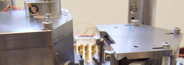
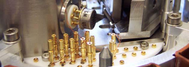
4 An Omicron STM/AFM system
5 Scanning tunneling microscopy Tip z profile Sample z piezo electron constant current mode: current is the feedback parameter I Amp V Log Amp Feedback Scanning Data proc. Error Set point By approaching the tip with a specified bias and current, the tip will be held a certain distance from the sample surface so that the specified current (set point) is realized. By scanning the tip across the sample under this condition, the system will compare the measured current I and the set point I s current (I-I s ) and uses this error signal as the feedback parameter to apply an appropriate voltage to the z-piezo to adjust the tipsample distance so as to diminish the error signal, thus providing the height profile of the topography of the surface. This is the constant current mode. The other operation mode is to keep the tip-sample distance while recording the current.
, they are used as scanner elements. Calibration against standards are necessary.")
6 Piezoelectric scanners Piezoelectric effect: electric field induced displacement of crystal and vice versa Lead zirconate titanate: PZT T>CT Powders are fired (1350º C) to form films. After polarization under an electric field (e.g., 60 kv/cm for an hour), they are used as scanner elements. Calibration against standards are necessary. T<CT Curie temperature ~ 350º Operated significantly below CT Unpoled During poling After poling

7 Vibration isolation is critical to achieve atomic resolution Combination of spring suspension and eddy current damping brings an optimum damping for STM.
8 Electron tunneling through a barrier Wavelike behavior governed by Schrödinger s equation h 2 2 ( + U) ψ( x) = Eψ( x) 2 2m x U E Electrons incident to the barrier 0 w x ψ 1 ( x) = Ae ikx + Be ikx k me = 2 h Wave number k Electrons within the barrier ψ ( x) = Ce + De = ψ ( ) e kx kx kx Tunneling constant κ 2m( U E) κ = h Probability of finding electrons on the other side of the barrier Electrons tunneling to the other side of the barrier ψ 3 ( x) = Fe ikx + Ge ikx k me = 2 h Wave number k 2 2 ψ 1 () 0 e 2mU ( E) w h Tunneling current scales exponentially with barrier width
9 Tunneling current between biased tip-sample Zero bias Negative sample bias Electrons below E f tunnels to tip sample Φ d E vac tip E sf sample tip E f ev E tf vacuum gap I ψ 1 () 0 e mφ w h V I Electrons in the sample with energy within E sf -ev to E sf tunnel into the tip above its E tf to E tf +ev. This tunneling of electrons will be measured by the circuit connecting the tip and sample and used as the feedback parameter.
 but no bias Sample negatively biased: Electrons from occupied states of sample tunnel to")
10 Local density of states By varying bias, the tunneling current is a measure of local density states for electrons Tip far away Sample positively biased: Electrons from tip tunnel to empty states of sample Tip close to sample (within tunneling distance) but no bias Sample negatively biased: Electrons from occupied states of sample tunnel to tip
11 Scanning tunneling spectroscopy P.G. Collins et.al., Phys. Rev. Lett. 82, 165 (1999)
12 Scanning tunneling spectroscopy K. W. Hipps, in Handbook of Applied Solid State Spectroscopy, ed. D. R. Vij, Springer, Berlin, Schematic diagram of Orbital Mediated Tunneling Spectroscopy and representative spectrum obtained from cobalt(ii) tetraphenylporphyrin in an STM under UHV conditions at room temperature. The central diagram shows resonant tunneling through unoccupied (upper) and occupied (lower) orbitals in positive and negative bias, respectively. This diagram works equally well for a M-I-M junction (base and top metal labels) and for an STM (tip and substrate labels).
13 Tunneling current sensitive to tip-sample distance: feedback parameter Current (arb. unit) I e Φ w With averaged work function ~4 ev, Φ in ev and w in Å I e 2w % of current from the protruded single atom Distance (Å) ~1.5 Å When tip-sample distance changes in 1 Å, the tunneling current will change times. A consequence of this sensitivity is the physics behind STM. Suppose an STM tip is terminated by a single atom (radius ~1.5 Å). The next atom is therefore ~2.6 Å away from the terminus atom, whose contribution is e -5.2 =0.6% of the current contributed by the terminus atom. This high sensitivity of current over distance makes STM an imaging tool having atomic resolution (of course with good tips and samples).
")
14 Tunneling resistance and current measured on Pt I = V R e m 2 2 Φ w h G. Binnig et.al., App. Phys. Lett. 40, (1982)

 1983 Phys. Rev. Lett.")
 Phys. Rev. Lett.")
15 STM accepted as capable of probing atoms in real space Being able to image Si (111) 7x7 STM breakthrough 7 x 7 silicon (111) 1983 Phys. Rev. Lett. 50, (1983) Pys.Rev. B 70, (2004) Phys. Rev. Lett. 90, (2004)

16 Standard test sample for atomic resolution on STM and AFM
 Chemical structure of DBTF molecules with experimental (B) and calculated (C) STM images (2.5 by 4.")
 STM image (5.9 by 3.")
17 L. Lafferentz et al., Science 27 February 2009: STM on polymerization of dibromoterfluorene on Au(111) Vol no. 5918, pp On-surface polymerization of DBTF to conjugated molecular chains. (A) Chemical structure of DBTF molecules with experimental (B) and calculated (C) STM images (2.5 by 4.5 nm) of intact molecules, with bright protrusions associated with the lateral dimethyl groups. (D) Overview STM image (80 by 120 nm, 1 V, and 0.1 na) after onsurface polymerization. The produced long covalently bound molecular chains, i.e., polyfluorene, follow the herringbone reconstruction of the substrate. (E) STM image (5.9 by 3.6 nm) of a single polyfluorene chain end with its chemical structure superimposed (using a different scaling). The arrows indicate three identical (in the STM image and the chemical structure), newly formed covalent bonds between individual building blocks. DBTF molecules (about 1/10 of a monolayer) were evaporated at a Knudsen cell temperature of about 500 K onto the Au(111) sample held at about 320 K.
 surface, they intermix with the substrate and locally lift the reconstruction, while submerging into the crystal.")
18 Metal nano wire Appl. Phys. Lett. 83, No. 22, 1 Dec When Pt atoms adsorb onto Ge(001) surface, they intermix with the substrate and locally lift the reconstruction, while submerging into the crystal. As a result of high temperature annealing of the Ge substrate at ~1000 K they partly re-appear at the surface, forming extremely well ordered nanowire arrays by self-organization. These wires are stable at room temperature. Scanning Tunneling Spectroscopy / Microscopy, shows they are metallic, kinkless and defect free. They are only 0.4 nm thin with a spacing of 1.6 nm in-between and have aspect ratios upto Besides patches of nanowires, individual ones with varying lengths are also common on the surface.
19 To achieve atomic resolution, an STM probe has to be effectively terminated by a single atom Tungsten tip: electrochemistry (anodic oxidation) in NaOH A Tungsten wire positively biased (relative to a circle of stainless steel wire) is thinned in NaOH through anodic oxidation and it eventually breaks by the weight of the lower part of the wire. Anodic oxidation W 4-12 V Annealing treatments are necessary to remove oxide left on the probe Still the overall probe size is tens of nanometers NaOH Scanning on surface, applying high voltage to the tip a single atom protruded on the tip apex Keep scanning and probably purposely crashing tip to sample surface Single atom terminating tip
20 STM AFM It is realized in the early days of STM that the tip impose forces on the sample when they are close to each other. This, plus the need to scan insulating samples, droved the effort in the invention of atomic force microscopy in 1985.
.")
21 Tunneling current & forces exerted on the probe: approach Shown here is the use of a tuning fork to measure both tunneling current and force. The tunneling current is measured as in STM and the force is measured by way of measuring resonance frequency change (details to come ). A very small oscillation amplitude must be used to avoid disturbing the tip-sample interaction (0.25 Å ).

22 Tunneling current & forces exerted on the probe: results STM is operated in the attractive force region Maximum attractive force ~2 nn
23 The first AFM The cantilever is a metal foil and the tip is a piece of diamond glued on the foil. Naturally, an STM tip was used to detect the deflection of the cantilever. The deflection detection scheme was soon replaced by optical lever detection.

24 Atomic force microscopy: force used as the feed back parameter
25 How AFM works... AFM images surface features of a sample by scanning a sharp tip attached to a cantilever. The basic principle for AFM is schematically shown on the right. The key point in AFM is the measurement of the interaction between the tip and surface features, which is sensed through the deflection of the cantilever using a laser beam. There are two operation modes for AFM: 1) Contact mode AFM---the tip is mechanically contacted with sample surface at an applied force. Lateral force detection in this mode can be used to probe local surface properties. 2) Dynamic force (tapping, non-contact) mode AFM---It is the oscillation amplitude (or phase) that is used as the feedback parameter to keep the tip-sample interaction constant. Surface can be imaged without (or with less) surface degradation due to the elimination of lateral force in this mode. Photodiode Monitoring interaction between tip and surface Contact mode Dynamic force (Non-contact) (Tapping) Tip Sample Laser diode Contact force Cantilever Oscillation amplitude Attached to scanner (x, y, z) Keeping it constant by adjusting the separation between tip and surface Height information

26 Contact mode AFM: tip contacts with sample T. Stifter et. al., Phys. Rev. B 62 (2000) Attractive forces: Capillary and van der Waals forces Repulsive forces: Overlapping of electron clouds (Coulomb interaction)
27 Interaction force between two atoms What is behind AFM? One can understand the interaction forces between the tip and the surface in AFM through the equation for Lennard- Jones potential w(r) = -A/r 6 + B/r 12, which deals with the interaction between two atoms. The force is thus F = - dw(r)/dr= -6A/r B/r 13. According to the text, A and B are known to be Jm 6 and Jm 12, respectively. We show the calculated results here in two regions: 1) around 0.4 nm a small attractive force is seen and 2) when the separation between the two atoms gets close to 0.2 nm the repulsive force increases steeply. Note the difference in force scale in the two figures. In practice, the AFM probe tip and the sample surface will have attractive force much larger than what is shown here. Also, other longer-range forces could occur. This is because the size of the tip is nominally ~10 nm nowadays and, in air, there are water films covering everything.
 of the cantilever.")
 and stiff cantilever (spring constant > 5 N/m) are used in contact and dynamic force AFM, respectively.")
28 AFM cantilevers A tip-cantilever sensor system The interaction between the sharp tip and the sample surface is detected by the deflection (contact mode AFM) or the oscillating amplitude (dynamic force mode AFM) of the cantilever. A photodiode is used to detect the movement of the cantilever from a laser beam irradiated on the cantilever. Two types of cantilever ~ 10 nm μm ~ 10 μm 0.6 ~ 4 μm Soft cantilever (spring constant < 1 N/m) and stiff cantilever (spring constant > 5 N/m) are used in contact and dynamic force AFM, respectively. The geometry of cantilever is schematically shown (width for both types is μm) between the two optical images for the two types of cantilever.


29 Cantilever detection of force exerted on tip Spring constant k = Ewt 3 4l 3 Force exerted F = kz Optical detection scheme: Laser and position sensitive photodetector Sensitivity: photodetector output deflection of cantilever (mv/nm)
30 Imaging mechanism of contact AFM A soft cantilever (<1 N/m) is usually used. The tip is in contact with the sample surface. Imaging force can be selected at the repulsive force region at a couple of nanonewton (nn). Morphology is obtained through scanning the surface at a constant force. During the scanning, the torsional movement of the cantilever can also be recorded, which results in lateral (friction) force imaging. This imaging technique provides information on friction force or chemical force distribution on the surface. With some modifications on AFM, resistance distribution and mechanical properties can be obtained simultaneously with the morphology. Contact mode AFM Force-distance curve Dotted line indicates imaging force Friction force detection A force-distance curve shown here was obtained on a UV/ozone modified polymer surface with a cantilever having spring constant of 0.03 N/m. Interaction between the tip and the surface at different separation is indicated by a-f. Adhesion force between the tip and sample due to their contact can be measured as shown in the forcedistance curve. Because the tip is in contact with the sample surface, damage on soft sample during scanning could happen. This can be largely avoided in the dynamic force mode AFM.

31 Adhesion force from force-distance curve Force-distance curves are obtained by extending the tip to the surface to make a contact between the tip and the sample surface followed by retracting the tip from the surface. The original point for the distance may be defined as the mechanical contact between the tip and surface in the extending cycle. Extending the tip beyond that point will result in load forces applied to the surface. The slope of t his load force is a measure of the Young's modulus of the surface, possibly mixed with the spring constant of the cantilever. As a result, a cantilever whose spring constant is comparable with the surface stiffness should be used to measure the elasticity information. In the retracting cycle, because of the adhesion properties between the tip and surface, the tip will not depart from the surface until the force used to pull the tip from the surface exceeds the adhesion force between them. This pull-off force can be considered as a measure of the adhesion force between the tip and surface. Adhesion force can be related to surface energies of the tip and sample surfaces, as well as their interfacial energy. Shown here is an example of measuring adhesion force at different regions on a polymer film. The striped areas have higher adhesion as well as friction forces than the normal surface. Topography MD Force (nn) a "Normal" Striped Counts b "Normal" Striped Friction force stripped normal μm Tip-sample separation (nm) Adhesion force (nn)


32 Examples of application of AFM Amphiphilicity of molecular layers 9 a) 5 2 Excessive amount of OPA molecules were observed to form bilayer and odd-numbered multilayers when their solution was placed on a silicon substrate followed by a heat treatment at EC. Our experimental facts indicated that a hydrophobic tailterminated surface is more favourable than a hydrophilic headgroup-terminated surface, though the hydrophilic headgroup terminated bilayer is the platform for other multilayers. Friction force imaging is a powerful means to distinguish the chemical amphiphilicity of molecular layers. Therefore, AFM provides a unique means for characterizing bilayer and multilayer formation on a support. 7 b) Topographic (a) and friction force (b) images (scan area: 14.0 µm 8.8 µm) showing bilayer and odd-numbered multilayers. Numbers shown in (a) indicate the number of molecular layer in the multilayers. Shown in (c) are profiles indicated by insert dotted lines in (a) and (b) for the height and friction force. The gray scale is 0 to 40 nm for (a) and 1.3 to 2.0 na for (b), respectively. The friction force was directly expressed by the output of the photodetector (photo-induced current in na units) corresponding to the torsional movement of the cantilever. Height (nm) c) Distance (μm) Friction force (arb. unit)

 than the unscratched area.")
33 Ozone-treated Examples of application of AFM Preferential oxidation on scratched areas Lateral force imaging and adhesion force measurement are used to investigate preferential oxidation on scratched areas. It is clear from the friction force image shown below (scan area is 6 μm square) that the shear-force deformed PP areas have higher friction force (and higher adhesion force) than the unscratched area. The images (scan area is 1 μm square) on the right column show clearly preferential oxidation caused by ozone treatment on the scratched area. Creating local active areas Unscratched Scratched Topography Friction force image Original
 and an increase in adhesion force.")
34 Examples of application of AFM Modification of Surface morphology Surface modification of polymer films AFM measurements clearly show formation of mounds on UV/ozone treated polypropylene (PP) film from the original surface characterized by fiberlike network structure (scan area is 2 μm square and height range is ~ 25 nm) and an increase in adhesion force. This increase in adhesion force indicates an increase in surface energy due to the oxidation of the modified polymer films. and energetics on polymer surfaces Adhesion force increase The adhesion force distribution for original and UV/ozone treated PP films shown below was obtained from force-distance measurements. It is clear that the adhesion force was increased with the UV/ozone treatment time. Original PP 15-min treated PP Original UV/ozone treated PP films 20 Counts min 3 min 15 min Adhesion force (nn)
35 Why adhesion force increases? Polypropylene (PP) CH CH 2 CH 3 CH CH 2 CH 3 CH CH 2 CH 3 Formation of polar (functional) groups by UV/ozone treatment Carbonyl Hydroxyl OH Carboxylic acid O CH CH 2 O C CH 2 CH 3 CH C CH 3 OH Unshared electron pair
36 Young s modulus estimated from force-distance curves With h being the piezo movement, p the deflection of the cantilever and d the penetration of the tip to sample. The cantilever s spring constant is k c and the force F exerted on the tip can be calculated from the cantilever deflection Hertzian model connects penetration, force, the radius of the probe, Young s moduli of probe and sample, as well as Poisson s ratio. The relationship between the force and piezo movement is thus: h = p+ d F = k p c [ ] Fh ( ) = k h dh ( ) 3 2 dh ( ) = Fh ( ) ( D / R) Fh ( ) = kc h Fh ( ) ( D / R) 2 c D = ( σ ) E E 1 3 s t h Fh ( ) = + k c Fh ( ) ( D / R) 1 3 By modulating distance and recording response of the cantilever under contact mode, modulus contrast mapping is possible.
37 Force Modulation technique to image elasticity distribution Cantilever oscillation over area 1 Cantilever oscillation over area 2 Photo diode position sensor for detection of cantilever oscillation via a lock-in amplifier, which is a measure of Young s modulus amplitude time 1 2 Bimorph amplitude time ~ Power source for sample oscillation amplitude time Sample stage oscillation


38 Force Modulation In contact mode AFM, together with the topographic feature, one can probe local elastic properties of materials through a mechanical interaction between the surface and tip. This can be done by oscillating the sample height while measuring the response of the cantilever with lock-in amplifier technique. In this technique, what is measured is the slope of a force-distance curve, which corresponds to elastic properties of the sample. Therefore elasticity difference on a surface can be distinguished by using this technique. Shown in figures to the left are topography (left) and elasticity (right) mapping for polystyrene (above) on a mica substrate and a polystyrene/polyethylene oxide blend film. Scan area is 5.25 and 3.75 μm square for the polystyrene and polystyrene/polyethylene oxide blend samples, respectively. Force-distance curves (a) obtained on the mica and the PS film and the simultaneously obtained response (b) of the cantilever to an oscillation of the sample height with an amplitude of 1 nm at 5 khz. The spring constant of the cantilever used was 18 N/m and the approaching and retracting speed for the tip was 3 nm/s. The difference seen for the cantilever response (b) is due to the different slope of the force-distance (a) curves on the different materials, which is a reflection of difference in Young s modulus for mica (200 GPa) and PS (5 GPa).
39 Dynamic force mode AFM Cantilever is oscillated and its changes in oscillation due to tip-sample interaction are used to probe surface morphology and properties.
40 Point mass spring model for AFM: Equation of motion for forced damped oscillation in free space mass m 2 d z 2 dt + c dz dt damping coefficient + kz = F 0 spring constant cosωt driving force quality factor ω 2 = 0 Q = k / m mk c c = m / Q ω 0 2 d z 2 dt ω0 + Q dz dt 2 + ω z 0 = F0 m cosωt z Steady state solution = Acos( ω t + φ) amplitude phase shift
41 Resonance frequency and phase lag (frequency sweep) A = Amplitude (arb. units) [( F ω 0 ω ) + / m ( ωω / Q) Frequency (khz) 2 ] 1/ 2 Q=500 ω 0 =300 khz k=40 N/m Phase (degree) tan( φ) = ωω / Q ω ω Frequency (khz)
42 Oscillating cantilever to detect force gradient between tip and sample Resonance frequency changes when there is force exerted to the tip: f 0 = 2π k m f = 2π k F + z m Causing changes in amplitude and phase lag. Thus, amplitude-modulation AFM and phase imaging. J. Appl. Phys. 69 (2), 15 January 1991 Δf = F k + z k m m f F F = + f kz + kz 2π 2π = f F 2kz
43 Imaging mechanism of dynamic force AFM Dynamic force (tapping, non-contact) mode AFM A stiff cantilever (~40 N/m) is oscillated around its resonant frequency (see the insert in the figure shown here). The tip is not in contact with (very small amplitude, say 1 nm; this is non-contact mode) or only taps (large amplitude, usually > 10 nm; this is tapping mode) the sample surface. That way, lateral dragging due to scanning is largely eliminated, effectively preventing soft sample surface from being damaged as could be using contact mode AFM. Information available from this mode: Morphology, phase imaging (due to differences in friction force, chemical force, adhesion force, mechanical properties). Amplitude-distance curve Dotted line indicates imaging condition (amplitude is damped to ~ 50 %) An amplitude-distance curve shown here was obtained on a polymer surface. Interaction between the tip and the surface at different separation is indicated by a-c. At part a, the tip is far away from the sample. After the tip is in contact with the sample (c), the cantilever no longer oscillates. Usually, surface is scanned by maintaining a reduced amplitude at 50 %.

44 Phase imaging In dynamic force mode AFM, phase shift between the sinusoidal voltage source applied to oscillate the cantilever and the actual oscillation of the cantilever can be effected by the interaction between the tip and the sample. The phase shift in the oscillating cantilever is related to tip-surface interaction which is basically material specific. Therefore, phase shift in tapping AFM can be used to distinguish different surface compositions on a surface (see the schematic below). There are many surface properties that may have an effect on the phase shift contrast. They could be differences in friction, viscoelasticity, adhesion, material, etc. Phase imaging usually gives clear contrast on a surface if there are any differences in surface properties as described above. Applications include visualizing phase separation in polymer blends, distinguishing different compositions on surface. Shown here is topography (left) and phase image (right) for a surface of a toner particle of carbon black matrix with polymer filler (scan area is 3.5 μm square) On area 1 Response Applied voltage On area 2 Phase difference between area 1 and 2


 3 NC 2 H 3 PO")

45 Phase imaging and imaging ToF-SIMS of rat neurons ToF-SIMS analysis of neurons of a sectioned rat brain film using an IONTOF instrument Animal samples were provided by the Autism Research Group at UWO led by D.F. MacFabe. The results shown in this slide were from a collaboration between Surface Science Western and the ARG. Intensity (counts) 5 x CH 3 PO 4 C 2 H 4 PO 4 NC 2 H 4 PO 4 CH 4 NC 2 H 4 PO 4 (CH 3 ) 3 NC 2 H 3 PO Mass (m/z) SIMS is a method of analyzing the mass/charge ratio of ionized particles produced from the sample upon bombardment of an energetic primary ion beam.
 and phase shift (b)")
.")
 negative secondary ion images of (d) CH, (e) CN")

 mode.")

46 Topography Phase shift ToF-SIMS a b c 5 µm CH +CN +PO 2 d CH e CN f PO 2 AFM topographic (a) and phase shift (b) images (22 μm 22 μm) for neurons in the CA1 field obtained on a sectioned rat brain film (thickness: 30 μm). The time-of-flight secondary ion mass spectrometry (ToF-SIMS) negative secondary ion images of (d) CH, (e) CN and (f) PO2 are overlapped in (c) where CH is plotted in blue, CN in green and PO2 in red, respectively. The ion images were measured using Bi+ primary ion beam with the high spatial resolution (burst alignment) mode. The ion images are plotted using 600 scans of data collection. The white lines inserted in (a)-(c) guide the eye to subcellular features imaged by both techniques.
47 Phase shift curves obtained with a cantilever of k = 2 N/m and Q = 150 on a silicon substrate N.F. Martinez and R. Garcia, Nanotechnology 17 (2006) S167 S172
48 Phase shift angle dissipation energy at tip-sample interaction Phase shift is sensitive to tip-sample interaction. This is why phase shift image is a powerful technique in differentiating component materials on a sample. According to Cleveland et al. and Garcia et al., phase shift angle φ is related to tipsample energy dissipation (E dis ) process (which in turn reveals difference in material properties) and hydrodynamic damping in the medium (E med ). In amplitude-modulated AFM with a cantilever oscillated at frequency ω (ω 0 being resonance frequency) having a free amplitude A 0 and setpoint A, the phase lag φ is ωa sin φ 1+ ω 0 A0 E = dis E med

49 Phase shift image and energy dissipation Molecular layers (Sexithienyl, T6) deposited on silicon E dis = sinφ A A A A 0 0 πka Q 2 0 Dissipation energy at different tip-sample separation normalized to free amplitude. N.F. Martinez and R. Garcia, Nanotechnology 17 (2006) S167 S172
50 Accuracy of AFM measurement: Convolution Convolution of tip geometry into measured features when tip apex radius is comparable with dimension of surface features. R=r R R ( ) ( ) 4 ( 2 ) x = R+ r R r = 4Rr c c R = Rr + R r R = c R + r r r x w R c w = 2 2Rh h = 2r R=10 nm R=5 nm R=20 nm w (nm) r (nm) θ When probe radius<<surface features, cone angle of the probe dominates the convolution.

 film, which contains nanometer-scale sized")
51 Accuracy of AFM measurement The morphology of a surface imaged by AFM is obtained through an interaction between the probe tip and surface features. When the tip is contaminated and the size of the contaminant is comparable to or larger than the size of the features on the sample surface, artefacts attributable to the contaminant are observed to dominate the image (see the following figure on the left-hand side: dotted lines represent the measured profiles). Here is a simple and effective method of evaluating tip performance by the imaging of a commercially available biaxially-oriented polypropylene (BOPP) film, which contains nanometer-scale sized fibers. The BOPP film surface is appropriate for use as a reference because a contaminated tip will not detect the fiber-like network structure. The very fine fiber-like structure of the BOPP film surface is a good criterion for the tip performance as shown in the following figure (right-hand side). Because the polymer film is soft compared to the silicon tip (Young's modulus for polypropylene is 1-2 GPa, while for silicon it is GPa), the polymer will not damage the tip when the tip is pushed into the polymer. This property can be used to clean a contaminated tip, i.e., by pushing the contaminated tip into the polymer, contaminants are most likely removed from the tip apex, probably to the side of the tip. Another important property of the BOPP is that the polymer film is highly hydrophobic and has a very low surface energy of ~ 30 mj/m 2 (The surface energy for Si is ~ 1400 mj/m 2 ; and the surface tension of water is 72 mj/m 2 ). These properties prevent contaminants from accumulating on the surface and hence prevent the contamination of the tip in the evaluation process.
- (d)]. These three images are obviously dominated by three different tip shapes.")

52 BOPP as a test sample to check AFM tip performance An AFM image (a) obtained on a BOPP film using a clean tip, reflecting the true morphology characterized by the fiber-like network structure. When damaged or contaminated AFM tips were used, the fiber-like features are no longer seen in the AFM images [ (b)- (d)]. These three images are obviously dominated by three different tip shapes. Comparison of the AFM images strongly suggests that the BOPP film can be used as a reference sample to check the performance of an AFM tip. The criterion is simple and straight forward: if the fiber-like features are revealed by an AFM tip, then the tip quality is sufficient to collect true images. An AFM tip can be easily contaminated or damaged depending on the chemical and mechanical properties of the sample surface it scans. It is therefore desirable to adopt a simple qualifying method such as this one using BOPP film to check the performance of the AFM tips to make sure the collected AFM images be meaningful. Only this image is true

.")

53 Cleaning contaminated tip on BOPP In order to prove that BOPP film is indeed useful for checking AFM tip performance, we managed to image the same area using the same tip when it was clean, after it had been contaminated and then after it was cleaned again. That way, any change in the AFM images obtained would be solely due to the contamination on the tip apex. AFM images shown in (a), (b) and (c) were obtained on the same area of a BOPP film using the same tip when it was clean, contaminated and re-cleaned, respectively. The tip was contaminated by being scanned on an organic acid coated Si substrate. It is clear that the image collected by the contaminated tip is dominated by tip effect (b). We cleaned the contaminated tip by pushing it into the polymer film, and its cleanliness is evidenced in AFM image shown in (c). Therefore, the use of the BOPP film to check the AFM tip performance and to clean the contaminated tip was successful. a b How to clean a contaminated tip The amplitude versus the tip-sample separation when the tip is brought to and retracted from the sample surface is represented by open and filled circles, respectively. For clarity only the first and fourth curves are shown here. The speed of the tip movement was 100 nm/s. c

54 Use of BOPP film: Application to blind tip reconstruction We have found that a BOPP film is suitable for checking tip performance and for cleaning contaminated tips, thus making it possible to collect images of the same area of a BOPP film surface before and after the tip was cleaned. Therefore, the difference between the two different images is solely due to the contamination of the tip. We took advantage of our ability to collect AFM images of the same area using the same tip, in one instance, contaminated and, in the other, after being cleaned. Commercial software SPIP (Metrology Image ApS, Denmark) was used to estimate the tip geometry using its tip characterization module, in which the blind reconstruction algorithm is implemented. First we used blind reconstruction on the image collected using the contaminated tip. Blind tip reconstruction allows one to extract the geometry of the tip from a given image. Once we had estimated the geometry of the contaminated tip, we used it to simulate the tip effect using the image collected using the cleaned tip. By comparing the simulation result with the image collected using the contaminated tip we showed that the blind reconstruction routine works well. Prior to this, there was no de facto method for testing blind reconstruction algorithms. It would be not only tedious but also difficult to verify the tip geometry from the blind reconstruction method with scanning electron microscopy (SEM) images. We proposed a simpler way to test blind reconstruction: comparison of AFM images collected in the same area of the BOPP by clean and contaminated tips. If the estimation of the contaminated tip geometry is reasonable, then one expects to be able to use the estimated tip geometry to dilate the image collected using the clean tip to obtain an image resembling one collected using the contaminated tip. This way, the verification of the estimated tip has proven easy and effective.
55 Techniques based on AFM Scanning surface potential microscopy Piezoelectric force microscopy Magnetic force microscopy Scanning thermal microscopy Multimodal AFM make use of dynamics and harmonics of oscillating cantilever Frequency-modulation AFM (in UHV for atomic resolution)

56 Scanning surface potential microscopy When there is a difference in potentials between the tip and sample surfaces, an oscillating electromagnetic force appears between the tip and sample surface at the frequency of the applied sinusoidal voltage, which makes the cantilever oscillate. This oscillation is used as the feedback parameter for the system which tries to stop this oscillation by applying a dc voltage to the tip (V t ) so as to make the potential difference between the tip and sample surfaces vanish (V t +V s =0). Thus the potential on the sample V s can be measured. Grounded Au Glass Biased Au Bias V Lift mode: scanning a line under tapping mode AFM to obtain profile, followed by repeating the same line scan with the tip lifted (e.g., 50 nm) with the AFM feedback being turned off and the SSPM feedback turned on. Photodiode Laser diode F ( V + V ) V sinωt t s ac Cantilever Attached to scanner (x, y, z) Lock-in amp. (ω) Tip Sample Cantilever Oscillation? V t ~ V ac sin(ωt)

57 An example of SSPM Application AFM image shows the device topology and SSPM image reveals significantly more information about the potential distribution and current flow through the nanowire. Specifically, the SSPM image shows that the electroactive defect created by the electron beam also includes the area of the neighboring oxide, which is evident as the white area in the center. This image also shows that the defect significantly modulates the potential distribution along its length of the nanowire, indicated by the sharp white-to-dark transition along its length. In fact, most of the potential drop is in the area of the defect and is due to a p-n junction, which the electron beam created in the nanowire. This result illustrates that the defect-creating technique can be used both to study and control the function of nanodevices.
58 Piezoresponse force microscopy Photodiode Laser diode Contact mode AFM Applying ac voltage to the tip Piezoeletric domain respond to the applied voltage by extracting or expanding; this mechanical response exerts forces to the contacted tip, resulting in detection of the deflection and torsion of the cantilever. Amplitude for strength and phase for polarization direction. This technique is used to detect ferroelectric domains as well as write on ferroelectric film. Lock-in amp. (ω) Def. Phase Tor. Amplitude Tip Cantilever Sample ~ V 0 sin(ωt) Amplitude Phase Out-of plane ferroelectric P In plane ferroelectric V 0 sin(ωt) Attached to scanner (x, y, z)
 images of a-c-domain structure in PbTiO 3 film. http://physics.unl.")
59 An example of PFM application Lateral PFM (a-amplitude, b-phase) and vertical PFM (c-amplitude, d-phase) images of a-c-domain structure in PbTiO 3 film.
 according to the thermal conductivity of material")
60 Scanning thermal microscopy Probe thermal conductivity over the scanned area with a tip capable of measuring temperature. By elevating the tip temperature slightly higher than the sample, the tip temperature will drop during scanning (in contact with the sample) according to the thermal conductivity of material component. Thermal image of a commercial carbon fibre Journal of Microscopy Volume 205, Issue 1, Pages (2002)

 was taken with LiftMode.")
61 Magnetic force microscopy Use of a magnetized probe to detect magnetic domains on the sample by detecting frequency/phase shift of the oscillating cantilever caused by magnetic force gradient from sample. Δf F = f 0 2kz Bits on a magneto-optical disk. The left image shows surface topography with tracks delineated by grooves. The magnetic force gradient map (right) was taken with LiftMode. Bit edge roughness is clearly visible, as is virgin domain structure in the grooves with features as small as 50nm. 5µm scan.

62 MFM on hard disk: revealing recorded bits Topography Frequency shift


63 Time-varying forces reconstructed from higher harmonics measurement Vertical vibration for feedback parameter to follow topography and torsional vibration for coefficients of Fourier transform (in frequency domain) to calculate back to time domain: time-resolved tip-sample interaction force. Torsional harmonic cantilever O. Sahin et. al., Nature Nanotechnology 2, (2007)
64 From frequency domain to time domain Frequency response and vibration spectra of a torsional harmonic cantilever Reconstructing tip-sample force waveform O. Sahin et. al., Nature Nanotechnology 2, (2007)
65 Reconstructed indentation force curves Deduced Young s moduli O. Sahin et. al., Nature Nanotechnology 2, (2007)
66 Frequency-modulation AFM Resonance frequency change is used as the feedback parameter to measure the surface. Rev. Modern Phys. 75, 949 (2003) Δf = F f 0 2kz H. Holscher et.al., Phys.Rev. B 61, (2000) Block diagram of the frequency-modulation AFM feedback loop for constant amplitude control and frequency-shift measurement.
 7x7 Atomic resolution routinely")
 www.afm.eei.eng.")
67 FM-AFM: Atomic resolution First non-contact AFM revealing Si(111) 7x7 Atomic resolution routinely obtained Si(111) 7x7 F. J. Giessibl, Science 267, 68 (1995)

68 Chemical identification of individual surface atoms by FM-AFM Frequency-modulation AFM in UHV allows precise measurement of attractive force. Y. Sugimoto et.al., Nature 446, (2007) Schematic illustration of AFM operation in dynamic mode (a), and of the onset of the chemical bonding between the outermost tip atom and a surface atom (highlighted by the green stick) that gives rise to the atomic contrast (b). However, the tip experiences not only the shortrange force associated with this chemical interaction, but also long-range force contributions that arise from van der Waals and electrostatic interactions between tip and surface (though the effect of the latter is usually minimized through appropriate choice of the experimental set-up). c, Curves obtained with analytical expressions for the van der Waals force, the short-range chemical interaction force, and the total force to illustrate their dependence on the absolute tip surface distance. d e, Dynamic force microscopy topographic images of a singleatomic layer of Sn (d) and Pb (e) grown, respectively, over a Si(111) substrate. At these surfaces, a small concentration of substitutional Si defects, characterized by a diminished topographic contrast, is usually found. The green arrows indicate atomic positions where force spectroscopic measurements were performed. Image dimensions are ( ) nm 2.


69 Difference in attractive forces leads to identification of atoms Nature 446, (1 March 2007)
70 SPM STM Atomic resolution Local density of states for electron Empty or filled electronic state imaging AFM Atomic resolution Probe various surface properties Platform for Nanotechnology
Basic Laboratory. Materials Science and Engineering. Atomic Force Microscopy (AFM)
") Basic Laboratory Materials Science and Engineering Atomic Force Microscopy (AFM) M108 Stand: 20.10.2015 Aim: Presentation of an application of the AFM for studying surface morphology. Inhalt 1.Introduction...
Basic Laboratory Materials Science and Engineering Atomic Force Microscopy (AFM) M108 Stand: 20.10.2015 Aim: Presentation of an application of the AFM for studying surface morphology. Inhalt 1.Introduction...
Lecture 4 Scanning Probe Microscopy (SPM)
") Lecture 4 Scanning Probe Microscopy (SPM) General components of SPM; Tip --- the probe; Cantilever --- the indicator of the tip; Tip-sample interaction --- the feedback system; Scanner --- piezoelectric
Lecture 4 Scanning Probe Microscopy (SPM) General components of SPM; Tip --- the probe; Cantilever --- the indicator of the tip; Tip-sample interaction --- the feedback system; Scanner --- piezoelectric
Program Operacyjny Kapitał Ludzki SCANNING PROBE TECHNIQUES - INTRODUCTION
 Program Operacyjny Kapitał Ludzki SCANNING PROBE TECHNIQUES - INTRODUCTION Peter Liljeroth Department of Applied Physics, Aalto University School of Science peter.liljeroth@aalto.fi Projekt współfinansowany
Instrumentation and Operation
 Instrumentation and Operation 1 STM Instrumentation COMPONENTS sharp metal tip scanning system and control electronics feedback electronics (keeps tunneling current constant) image processing system data
Scanning Probe Microscopy. Amanda MacMillan, Emmy Gebremichael, & John Shamblin Chem 243: Instrumental Analysis Dr. Robert Corn March 10, 2010
 Scanning Probe Microscopy Amanda MacMillan, Emmy Gebremichael, & John Shamblin Chem 243: Instrumental Analysis Dr. Robert Corn March 10, 2010 Scanning Probe Microscopy High-Resolution Surface Analysis
Scanning Tunneling Microscopy
 Scanning Tunneling Microscopy References: 1. G. Binnig, H. Rohrer, C. Gerber, and Weibel, Phys. Rev. Lett. 49, 57 (1982); and ibid 50, 120 (1983). 2. J. Chen, Introduction to Scanning Tunneling Microscopy,
Atomic Force Microscopy imaging and beyond
 Atomic Force Microscopy imaging and beyond Arif Mumtaz Magnetism and Magnetic Materials Group Department of Physics, QAU Coworkers: Prof. Dr. S.K.Hasanain M. Tariq Khan Alam Imaging and beyond Scanning
Scanning Probe Microscopy (SPM)
") CHEM53200: Lecture 9 Scanning Probe Microscopy (SPM) Major reference: 1. Scanning Probe Microscopy and Spectroscopy Edited by D. Bonnell (2001). 2. A practical guide to scanning probe microscopy by Park
CHEM53200: Lecture 9 Scanning Probe Microscopy (SPM) Major reference: 1. Scanning Probe Microscopy and Spectroscopy Edited by D. Bonnell (2001). 2. A practical guide to scanning probe microscopy by Park
NIS: what can it be used for?
 AFM @ NIS: what can it be used for? Chiara Manfredotti 011 670 8382/8388/7879 chiara.manfredotti@to.infn.it Skype: khiaram 1 AFM: block scheme In an Atomic Force Microscope (AFM) a micrometric tip attached
Lecture 12: Biomaterials Characterization in Aqueous Environments
 3.051J/20.340J 1 Lecture 12: Biomaterials Characterization in Aqueous Environments High vacuum techniques are important tools for characterizing surface composition, but do not yield information on surface
STM: Scanning Tunneling Microscope
 STM: Scanning Tunneling Microscope Basic idea STM working principle Schematic representation of the sample-tip tunnel barrier Assume tip and sample described by two infinite plate electrodes Φ t +Φ s =
Intermittent-Contact Mode Force Microscopy & Electrostatic Force Microscopy (EFM)
") WORKSHOP Nanoscience on the Tip Intermittent-Contact Mode Force Microscopy & Electrostatic Force Microscopy (EFM) Table of Contents: 1. Motivation... 1. Simple Harmonic Motion... 1 3. AC-Mode Imaging...
WORKSHOP Nanoscience on the Tip Intermittent-Contact Mode Force Microscopy & Electrostatic Force Microscopy (EFM) Table of Contents: 1. Motivation... 1. Simple Harmonic Motion... 1 3. AC-Mode Imaging...
Scanning Tunneling Microscopy
 Scanning Tunneling Microscopy Scanning Direction References: Classical Tunneling Quantum Mechanics Tunneling current Tunneling current I t I t (V/d)exp(-Aφ 1/2 d) A = 1.025 (ev) -1/2 Å -1 I t = 10 pa~10na
Scanning Probe Microscopy (SPM)
") Scanning Probe Microscopy (SPM) Scanning Tunneling Microscopy (STM) --- G. Binnig, H. Rohrer et al, (1982) Near-Field Scanning Optical Microscopy (NSOM) --- D. W. Pohl (1982) Atomic Force Microscopy (AFM)
Scanning Probe Microscopy (SPM) Scanning Tunneling Microscopy (STM) --- G. Binnig, H. Rohrer et al, (1982) Near-Field Scanning Optical Microscopy (NSOM) --- D. W. Pohl (1982) Atomic Force Microscopy (AFM)
MS482 Materials Characterization ( 재료분석 ) Lecture Note 11: Scanning Probe Microscopy. Byungha Shin Dept. of MSE, KAIST
 Lecture Note 11: Scanning Probe Microscopy. Byungha Shin Dept. of MSE, KAIST") 2015 Fall Semester MS482 Materials Characterization ( 재료분석 ) Lecture Note 11: Scanning Probe Microscopy Byungha Shin Dept. of MSE, KAIST 1 Course Information Syllabus 1. Overview of various characterization
2015 Fall Semester MS482 Materials Characterization ( 재료분석 ) Lecture Note 11: Scanning Probe Microscopy Byungha Shin Dept. of MSE, KAIST 1 Course Information Syllabus 1. Overview of various characterization
Scanning Force Microscopy
 Scanning Force Microscopy Roland Bennewitz Rutherford Physics Building 405 Phone 398-3058 roland.bennewitz@mcgill.ca Scanning Probe is moved along scan lines over a sample surface 1 Force Microscopy Data
General concept and defining characteristics of AFM. Dina Kudasheva Advisor: Prof. Mary K. Cowman
 General concept and defining characteristics of AFM Dina Kudasheva Advisor: Prof. Mary K. Cowman Overview Introduction History of the SPM invention Technical Capabilities Principles of operation Examples
Scanning Force Microscopy II
 Scanning Force Microscopy II Measurement modes Magnetic force microscopy Artifacts Lars Johansson 1 SFM - Forces Chemical forces (short range) Van der Waals forces Electrostatic forces (long range) Capillary
Contents. What is AFM? History Basic principles and devices Operating modes Application areas Advantages and disadvantages
 Contents What is AFM? History Basic principles and devices Operating modes Application areas Advantages and disadvantages Figure1: 2004 Seth Copen Goldstein What is AFM? A type of Scanning Probe Microscopy
Atomic Force Microscopy (AFM) Part I
 Part I") Atomic Force Microscopy (AFM) Part I CHEM-L2000 Eero Kontturi 6 th March 2018 Lectures on AFM Part I Principles and practice Imaging of native materials, including nanocellulose Part II Surface force measurements
Atomic Force Microscopy (AFM) Part I CHEM-L2000 Eero Kontturi 6 th March 2018 Lectures on AFM Part I Principles and practice Imaging of native materials, including nanocellulose Part II Surface force measurements
Module 26: Atomic Force Microscopy. Lecture 40: Atomic Force Microscopy 3: Additional Modes of AFM
 Module 26: Atomic Force Microscopy Lecture 40: Atomic Force Microscopy 3: Additional Modes of AFM 1 The AFM apart from generating the information about the topography of the sample features can be used
Characterization of MEMS Devices
 MEMS: Characterization Characterization of MEMS Devices Prasanna S. Gandhi Assistant Professor, Department of Mechanical Engineering, Indian Institute of Technology, Bombay, Recap Characterization of MEMS
Outline Scanning Probe Microscope (SPM)
") AFM Outline Scanning Probe Microscope (SPM) A family of microscopy forms where a sharp probe is scanned across a surface and some tip/sample interactions are monitored Scanning Tunneling Microscopy (STM)
AFM Outline Scanning Probe Microscope (SPM) A family of microscopy forms where a sharp probe is scanned across a surface and some tip/sample interactions are monitored Scanning Tunneling Microscopy (STM)
INTRODUCTION TO SCA\ \I\G TUNNELING MICROSCOPY
 INTRODUCTION TO SCA\ \I\G TUNNELING MICROSCOPY SECOND EDITION C. JULIAN CHEN Department of Applied Physics and Applied Mathematics, Columbia University, New York OXFORD UNIVERSITY PRESS Contents Preface
Scanning Probe Microscopy. EMSE-515 F. Ernst
 Scanning Probe Microscopy EMSE-515 F. Ernst 1 Literature 2 3 Scanning Probe Microscopy: The Lab on a Tip by Ernst Meyer,Ans Josef Hug,Roland Bennewitz 4 Scanning Probe Microscopy and Spectroscopy : Theory,
Imaging Methods: Scanning Force Microscopy (SFM / AFM)
") Imaging Methods: Scanning Force Microscopy (SFM / AFM) The atomic force microscope (AFM) probes the surface of a sample with a sharp tip, a couple of microns long and often less than 100 Å in diameter.
Imaging Methods: Scanning Force Microscopy (SFM / AFM) The atomic force microscope (AFM) probes the surface of a sample with a sharp tip, a couple of microns long and often less than 100 Å in diameter.
Techniken der Oberflächenphysik (Techniques of Surface Physics)
") Techniken der Oberflächenphysik (Techniques of Surface Physics) Prof. Yong Lei & Dr. Yang Xu Fachgebiet 3D-Nanostrukturierung, Institut für Physik Contact: yong.lei@tu-ilmenau.de yang.xu@tu-ilmenau.de
Techniken der Oberflächenphysik (Techniques of Surface Physics) Prof. Yong Lei & Dr. Yang Xu Fachgebiet 3D-Nanostrukturierung, Institut für Physik Contact: yong.lei@tu-ilmenau.de yang.xu@tu-ilmenau.de
Atomic and molecular interactions. Scanning probe microscopy.
 Atomic and molecular interactions. Scanning probe microscopy. Balázs Kiss Nanobiotechnology and Single Molecule Research Group, Department of Biophysics and Radiation Biology 27. November 2013. 2 Atomic
And Manipulation by Scanning Probe Microscope
 Basic 15 Nanometer Scale Measurement And Manipulation by Scanning Probe Microscope Prof. K. Fukuzawa Dept. of Micro/Nano Systems Engineering Nagoya University I. Basics of scanning probe microscope Basic
Today s SPM in Nanotechnology
 Today s SPM in Nanotechnology An introduction for Advanced Applications Qun (Allen) Gu, Ph.D., AFM Scientist, Pacific Nanotechnology IEEE Bay Area Nanotechnology Council, August, 2007 8/17/2015 1 Content
SOLID STATE PHYSICS PHY F341. Dr. Manjuladevi.V Associate Professor Department of Physics BITS Pilani
 SOLID STATE PHYSICS PHY F341 Dr. Manjuladevi.V Associate Professor Department of Physics BITS Pilani 333031 manjula@bits-pilani.ac.in Characterization techniques SEM AFM STM BAM Outline What can we use
Introduction to Scanning Probe Microscopy Zhe Fei
 Introduction to Scanning Probe Microscopy Zhe Fei Phys 590B, Apr. 2019 1 Outline Part 1 SPM Overview Part 2 Scanning tunneling microscopy Part 3 Atomic force microscopy Part 4 Electric & Magnetic force
Lecture 26 MNS 102: Techniques for Materials and Nano Sciences
 Lecture 26 MNS 102: Techniques for Materials and Nano Sciences Reference: #1 C. R. Brundle, C. A. Evans, S. Wilson, "Encyclopedia of Materials Characterization", Butterworth-Heinemann, Toronto (1992),
AFM for Measuring Surface Topography and Forces
 ENB 2007 07.03.2007 AFM for Measuring Surface Topography and Forces Andreas Fery Scanning Probe : What is it and why do we need it? AFM as a versatile tool for local analysis and manipulation Dates Course
Measurement of hardness, surface potential, and charge distribution with dynamic contact mode electrostatic force microscope
 REVIEW OF SCIENTIFIC INSTRUMENTS VOLUME 70, NUMBER 3 MARCH 1999 Measurement of hardness, surface potential, and charge distribution with dynamic contact mode electrostatic force microscope J. W. Hong,
Scanning Tunneling Microscopy Studies of the Ge(111) Surface
 Surface") VC Scanning Tunneling Microscopy Studies of the Ge(111) Surface Anna Rosen University of California, Berkeley Advisor: Dr. Shirley Chiang University of California, Davis August 24, 2007 Abstract: This
VC Scanning Tunneling Microscopy Studies of the Ge(111) Surface Anna Rosen University of California, Berkeley Advisor: Dr. Shirley Chiang University of California, Davis August 24, 2007 Abstract: This
Nitride HFETs applications: Conductance DLTS
 Nitride HFETs applications: Conductance DLTS The capacitance DLTS cannot be used for device trap profiling as the capacitance for the gate will be very small Conductance DLTS is similar to capacitance
CNPEM Laboratório de Ciência de Superfícies
 Investigating electrical charged samples by scanning probe microscopy: the influence to magnetic force microscopy and atomic force microscopy phase images. Carlos A. R. Costa, 1 Evandro M. Lanzoni, 1 Maria
Scanning Tunneling Microscopy
 Scanning Tunneling Microscopy A scanning tunneling microscope (STM) is an instrument for imaging surfaces at the atomic level. Its development in 1981 earned its inventors, Gerd Binnig and Heinrich Rohrer
Atomic force microscopy study of polypropylene surfaces treated by UV and ozone exposure: modification of morphology and adhesion force
 Ž. Applied Surface Science 144 145 1999 627 632 Atomic force microscopy study of polypropylene surfaces treated by UV and ozone exposure: modification of morphology and adhesion force H.-Y. Nie ), M.J.
Supporting information
 Electronic Supplementary Material (ESI) for Nanoscale. This journal is The Royal Society of Chemistry 2014 Supporting information Self-assembled nanopatch with peptide-organic multilayers and mechanical
Lorentz Contact Resonance for viscoelastic measurements of polymer blends
 The world leader in nanoscale IR spectroscopy for viscoelastic measurements of polymer blends (LCR) reliably compares viscoleastic properties with nanoscale spatial resolution With no moving parts in the
Introduction to Scanning Probe Microscopy
 WORKSHOP Nanoscience on the Tip Introduction to Scanning Probe Microscopy Table of Contents: 1 Historic Perspectives... 1 2 Scanning Force Microscopy (SFM)... 2 2.1. Contact Mode... 2 2.2. AC Mode Imaging...
Chapter 10. Nanometrology. Oxford University Press All rights reserved.
 Chapter 10 Nanometrology Oxford University Press 2013. All rights reserved. 1 Introduction Nanometrology is the science of measurement at the nanoscale level. Figure illustrates where nanoscale stands
MSE 321 Structural Characterization
 Auger Spectroscopy Auger Electron Spectroscopy (AES) Scanning Auger Microscopy (SAM) Incident Electron Ejected Electron Auger Electron Initial State Intermediate State Final State Physical Electronics
Lorentz Contact Resonance for viscoelastic measurements of polymer blends
 The nanoscale spectroscopy company The world leader in nanoscale IR spectroscopy Lorentz Contact Resonance for viscoelastic measurements of polymer blends Lorentz Contact Resonance (LCR) reliably compares
Scanning Tunneling Microscopy
 Scanning Tunneling Microscopy References: 1. G. Binnig, H. Rohrer, C. Gerber, and Weibel, Phys. Rev. Lett. 49, 57 (1982); and ibid 50, 120 (1983). 2. J. Chen, Introduction to Scanning Tunneling Microscopy,
SUPPLEMENTARY NOTES Supplementary Note 1: Fabrication of Scanning Thermal Microscopy Probes
 SUPPLEMENTARY NOTES Supplementary Note 1: Fabrication of Scanning Thermal Microscopy Probes Fabrication of the scanning thermal microscopy (SThM) probes is summarized in Supplementary Fig. 1 and proceeds
Supporting Information
 Supporting Information Analysis Method for Quantifying the Morphology of Nanotube Networks Dusan Vobornik*, Shan Zou and Gregory P. Lopinski Measurement Science and Standards, National Research Council
Experimental methods in physics. Local probe microscopies I
 Experimental methods in physics Local probe microscopies I Scanning tunnelling microscopy (STM) Jean-Marc Bonard Academic year 09-10 1. Scanning Tunneling Microscopy 1.1. Introduction Image of surface
AFM: Atomic Force Microscopy II
 AM: Atomic orce Microscopy II Jan Knudsen The MAX IV laboratory & Division of synchrotron radiation research K522-523 (Sljus) 4 th of May, 2018 http://www.sljus.lu.se/staff/rainer/spm.htm Last time: The
= 6 (1/ nm) So what is probability of finding electron tunneled into a barrier 3 ev high?
 So what is probability of finding electron tunneled into a barrier 3 ev high?") STM STM With a scanning tunneling microscope, images of surfaces with atomic resolution can be readily obtained. An STM uses quantum tunneling of electrons to map the density of electrons on the surface
STM STM With a scanning tunneling microscope, images of surfaces with atomic resolution can be readily obtained. An STM uses quantum tunneling of electrons to map the density of electrons on the surface
Introduction to Scanning Tunneling Microscopy
 Introduction to Scanning Tunneling Microscopy C. JULIAN CHEN IBM Research Division Thomas J. Watson Research Center Yorktown Heights, New York New York Oxford OXFORD UNIVERSITY PRESS 1993 CONTENTS List
Point mass approximation. Rigid beam mechanics. spring constant k N effective mass m e. Simple Harmonic Motion.. m e z = - k N z
 Free end Rigid beam mechanics Fixed end think of cantilever as a mass on a spring Point mass approximation z F Hooke s law k N = F / z This is beam mechanics, standard in engineering textbooks. For a rectangular
AFM Imaging In Liquids. W. Travis Johnson PhD Agilent Technologies Nanomeasurements Division
 AFM Imaging In Liquids W. Travis Johnson PhD Agilent Technologies Nanomeasurements Division Imaging Techniques: Scales Proteins 10 nm Bacteria 1μm Red Blood Cell 5μm Human Hair 75μm Si Atom Spacing 0.4nm
Scanning tunneling microscopy
 IFM The Department of Physics, Chemistry and Biology Lab 72 in TFFM08 Scanning tunneling microscopy NAME PERS. - NUMBER DATE APPROVED Rev. Dec 2006 Ivy Razado Aug 2014 Tuomas Hänninen Contents 1 Introduction
REPORT ON SCANNING TUNNELING MICROSCOPE. Course ME-228 Materials and Structural Property Correlations Course Instructor Prof. M. S.
 REPORT ON SCANNING TUNNELING MICROSCOPE Course ME-228 Materials and Structural Property Correlations Course Instructor Prof. M. S. Bobji Submitted by Ankush Kumar Jaiswal (09371) Abhay Nandan (09301) Sunil
From nanophysics research labs to cell phones. Dr. András Halbritter Department of Physics associate professor
 From nanophysics research labs to cell phones Dr. András Halbritter Department of Physics associate professor Curriculum Vitae Birth: 1976. High-school graduation: 1994. Master degree: 1999. PhD: 2003.
(Scanning Probe Microscopy)
") (Scanning Probe Microscopy) Ing-Shouh Hwang (ishwang@phys.sinica.edu.tw) Institute of Physics, Academia Sinica, Taipei, Taiwan References 1. G. Binnig, H. Rohrer, C. Gerber, and Weibel, Phys. Rev. Lett.
(Scanning Probe Microscopy) Ing-Shouh Hwang (ishwang@phys.sinica.edu.tw) Institute of Physics, Academia Sinica, Taipei, Taiwan References 1. G. Binnig, H. Rohrer, C. Gerber, and Weibel, Phys. Rev. Lett.
tip of a current tip and the sample. Components: 3. Coarse sample-to-tip isolation system, and
 SCANNING TUNNELING MICROSCOPE Brief history: Heinrich Rohrer and Gerd K. Binnig, scientists at IBM's Zurich Research Laboratory in Switzerland, are awarded the 1986 Nobel Prize in physicss for their work
Fundamentals of Atomic Force Microscopy Part 2: Dynamic AFM Methods
 Fundamentals of tomic Force Microscopy Part 2: Dynamic FM Methods Week 2, Lecture 5 ttractive and repulsive regimes and phase contrast in amplitude modulation FM rvind Raman Mechanical Engineering Birck
Improving the accuracy of Atomic Force Microscope based nanomechanical measurements. Bede Pittenger Bruker Nano Surfaces, Santa Barbara, CA, USA
 Improving the accuracy of Atomic Force Microscope based nanomechanical measurements Bede Pittenger Bruker Nano Surfaces, Santa Barbara, CA, USA How can we improve accuracy in our nanomechanical measurements?
Scanning Tunneling Microscopy
 Scanning Tunneling Microscopy References: 1. G. Binnig, H. Rohrer, C. Gerber, and Weibel, Phys. Rev. Lett. 49, 57 (1982); and ibid 50, 120 (1983). 2. J. Chen, Introduction to Scanning Tunneling Microscopy,
MSE 321 Structural Characterization
 Auger Spectroscopy Auger Electron Spectroscopy (AES) Scanning Auger Microscopy (SAM) Incident Electron Ejected Electron Auger Electron Initial State Intermediate State Final State Physical Electronics
Molecular and carbon based electronic systems
 Molecular and carbon based electronic systems Single molecule deposition and properties on surfaces Bottom Up Top Down Fundamental Knowledge & Functional Devices Thilo Glatzel, thilo.glatzel@unibas.ch
Chapter 2 Correlation Force Spectroscopy
 Chapter 2 Correlation Force Spectroscopy Correlation Force Spectroscopy: Rationale In principle, the main advantage of correlation force spectroscopy (CFS) over onecantilever atomic force microscopy (AFM)
Force-distance studies with piezoelectric tuning forks below 4.2K
 submitted to APPLIED SURFACE SCIENCE nc-afm 99, Pontresina Force-distance studies with piezoelectric tuning forks below 4.2K J. Rychen, T. Ihn, P. Studerus, A. Herrmann, K. Ensslin Solid State Physics
Microscopie a stilo: principi ed esempi di applicazione
 Microscopie a stilo: principi ed esempi di applicazione Adele Sassella Dipartimento di Scienza dei Materiali Università degli Studi di Milano Bicocca adele.sassella@unimib.it Pavia, 22 aprile 2009 SCANNING
Scanning Probe Microscopy
 1 Scanning Probe Microscopy Dr. Benjamin Dwir Laboratory of Physics of Nanostructures (LPN) Benjamin.dwir@epfl.ch PH.D3.344 Outline: Introduction: What is SPM, history STM AFM Image treatment Advanced
STM spectroscopy (STS)
") STM spectroscopy (STS) di dv 4 e ( E ev, r) ( E ) M S F T F Basic concepts of STS. With the feedback circuit open the variation of the tunneling current due to the application of a small oscillating voltage
STM spectroscopy (STS) di dv 4 e ( E ev, r) ( E ) M S F T F Basic concepts of STS. With the feedback circuit open the variation of the tunneling current due to the application of a small oscillating voltage
Magnetic Force Microscopy (MFM) F = µ o (m )H
 F = µ o (m )H") Magnetic Force Microscopy (MFM) F = µ o (m )H 1. MFM is based on the use of a ferromagnetic tip as a local field sensor. Magnetic interaction between the tip and the surface results in a force acting on
Magnetic Force Microscopy (MFM) F = µ o (m )H 1. MFM is based on the use of a ferromagnetic tip as a local field sensor. Magnetic interaction between the tip and the surface results in a force acting on
Studies of the Properties of Designed Nanoparticles Using Atomic Force Microscopy
 Louisiana State University LSU Digital Commons LSU Doctoral Dissertations Graduate School 2016 Studies of the Properties of Designed Nanoparticles Using Atomic Force Microscopy Steve Matthew Deese Louisiana
Scanning Probe Microscopy (SPM)
") http://ww2.sljus.lu.se/staff/rainer/spm.htm Scanning Probe Microscopy (FYST42 / FAFN30) Scanning Probe Microscopy (SPM) overview & general principles March 23 th, 2018 Jan Knudsen, room K522, jan.knudsen@sljus.lu.se
http://ww2.sljus.lu.se/staff/rainer/spm.htm Scanning Probe Microscopy (FYST42 / FAFN30) Scanning Probe Microscopy (SPM) overview & general principles March 23 th, 2018 Jan Knudsen, room K522, jan.knudsen@sljus.lu.se
CHARACTERIZATION of NANOMATERIALS KHP
 CHARACTERIZATION of NANOMATERIALS Overview of the most common nanocharacterization techniques MAIN CHARACTERIZATION TECHNIQUES: 1.Transmission Electron Microscope (TEM) 2. Scanning Electron Microscope
Lecture Note October 1, 2009 Nanostructure characterization techniques
 Lecture Note October 1, 29 Nanostructure characterization techniques UT-Austin PHYS 392 T, unique # 5977 ME 397 unique # 1979 CHE 384, unique # 151 Instructor: Professor C.K. Shih Subjects: Applications
Scanning Tunneling Microscopy. how does STM work? the quantum mechanical picture example of images how can we understand what we see?
 Scanning Tunneling Microscopy how does STM work? the quantum mechanical picture example of images how can we understand what we see? Observation of adatom diffusion with a field ion microscope Scanning
Integrating MEMS Electro-Static Driven Micro-Probe and Laser Doppler Vibrometer for Non-Contact Vibration Mode SPM System Design
 Tamkang Journal of Science and Engineering, Vol. 12, No. 4, pp. 399 407 (2009) 399 Integrating MEMS Electro-Static Driven Micro-Probe and Laser Doppler Vibrometer for Non-Contact Vibration Mode SPM System
Nanostructure. Materials Growth Characterization Fabrication. More see Waser, chapter 2
 Nanostructure Materials Growth Characterization Fabrication More see Waser, chapter 2 Materials growth - deposition deposition gas solid Physical Vapor Deposition Chemical Vapor Deposition Physical Vapor
Chapter 12. Nanometrology. Oxford University Press All rights reserved.
 Chapter 12 Nanometrology Introduction Nanometrology is the science of measurement at the nanoscale level. Figure illustrates where nanoscale stands in relation to a meter and sub divisions of meter. Nanometrology
Enrico Gnecco Department of Physics. University of Basel, Switzerland
 AOSCIECES AD AOTECHOOGIES anotribology - Enrico Gnecco AOTRIBOOGY Enrico Gnecco Department of Physics. University of Basel, Switzerland Keywords: Atomic stick-slip, Friction force microscopy, oad dependence
Nanoelectronics 09. Atsufumi Hirohata Department of Electronics. Quick Review over the Last Lecture
 Nanoelectronics 09 Atsufumi Hirohata Department of Electronics 13:00 Monday, 12/February/2018 (P/T 006) Quick Review over the Last Lecture ( Field effect transistor (FET) ): ( Drain ) current increases
Review. Surfaces of Biomaterials. Characterization. Surface sensitivity
 Surfaces of Biomaterials Three lectures: 1.23.05 Surface Properties of Biomaterials 1.25.05 Surface Characterization 1.27.05 Surface and Protein Interactions Review Bulk Materials are described by: Chemical
PY5020 Nanoscience Scanning probe microscopy
 PY500 Nanoscience Scanning probe microscopy Outline Scanning tunnelling microscopy (STM) - Quantum tunnelling - STM tool - Main modes of STM Contact probes V bias Use the point probes to measure the local
3.1 Electron tunneling theory
 Scanning Tunneling Microscope (STM) was invented in the 80s by two physicists: G. Binnig and H. Rorher. They got the Nobel Prize a few years later. This invention paved the way for new possibilities in
Simple Harmonic Motion and Damping
 Simple Harmonic Motion and Damping Marie Johnson Cabrices Chamblee Charter High School Background: Atomic Force Microscopy, or AFM, is used to characterize materials. It is used to measure local properties,
Università degli Studi di Bari "Aldo Moro"
 Università degli Studi di Bari "Aldo Moro" Table of contents 1. Introduction to Atomic Force Microscopy; 2. Introduction to Raman Spectroscopy; 3. The need for a hybrid technique Raman AFM microscopy;
Citation for published version (APA): Mendoza, S. M. (2007). Exploiting molecular machines on surfaces s.n.
: Mendoza, S. M. (2007). Exploiting molecular machines on surfaces s.n.") University of Groningen Exploiting molecular machines on surfaces Mendoza, Sandra M IMPORTANT NOTE: You are advised to consult the publisher's version (publisher's PDF) if you wish to cite from it. Please
University of Groningen Exploiting molecular machines on surfaces Mendoza, Sandra M IMPORTANT NOTE: You are advised to consult the publisher's version (publisher's PDF) if you wish to cite from it. Please
COURSE OUTLINE. Introduction Signals and Noise Filtering Sensors: Piezoelectric Force Sensors. Sensors, Signals and Noise 1
 Sensors, Signals and Noise 1 COURSE OUTLINE Introduction Signals and Noise Filtering Sensors: Piezoelectric Force Sensors Piezoelectric Force Sensors 2 Piezoelectric Effect and Materials Piezoelectric
Supplementary Information. Characterization of nanoscale temperature fields during electromigration of nanowires
 Supplementary Information Characterization of nanoscale temperature fields during electromigration of nanowires Wonho Jeong,, Kyeongtae Kim,, *, Youngsang Kim,, Woochul Lee,, *, Pramod Reddy Department
Measurements of interaction forces in (biological) model systems
 model systems") Measurements of interaction forces in (biological) model systems Marina Ruths Department of Chemistry, UMass Lowell What can force measurements tell us about a system? Depending on the technique, we might
Measurements of interaction forces in (biological) model systems Marina Ruths Department of Chemistry, UMass Lowell What can force measurements tell us about a system? Depending on the technique, we might
Scanning Probe Microscopy. L. J. Heyderman
 1 Scanning Probe Microscopy 2 Scanning Probe Microscopy If an atom was as large as a ping-pong ball......the tip would have the size of the Matterhorn! 3 Magnetic Force Microscopy Stray field interaction
AFM Studies of Pristine PCBM Changes Under Light Exposure. Erin Chambers
 AFM Studies of Pristine PCBM Changes Under Light Exposure Erin Chambers Faculty of health, science, and technology Department of engineering and physics 15 cr Krister Svensson Lars Johansson 28 March 2013
Application of electrostatic force microscopy in nanosystem diagnostics
 Materials Science, Vol., No. 3, 003 Application of electrostatic force microscopy in nanosystem diagnostics TEODOR P. GOTSZALK *, PIOTR GRABIEC, IVO W. RANGELOW 3 Fulty of Microsystem Electronics and Photonics,
Spectroscopy at nanometer scale
 Spectroscopy at nanometer scale 1. Physics of the spectroscopies 2. Spectroscopies for the bulk materials 3. Experimental setups for the spectroscopies 4. Physics and Chemistry of nanomaterials Various
Noncontact-AFM (nc-afm)
") Noncontact-AFM (nc-afm) Quantitative understanding of nc-afm A attractive interaction Δf Resonance frequency: f 0 Width of resonance curve (FWHM): Γ Γ+ΔΓ Γ Q-factor: Q π f Γ = 0 f 0 f Conservative forces
Noncontact-AFM (nc-afm) Quantitative understanding of nc-afm A attractive interaction Δf Resonance frequency: f 0 Width of resonance curve (FWHM): Γ Γ+ΔΓ Γ Q-factor: Q π f Γ = 0 f 0 f Conservative forces
Noncontact lateral-force gradient measurement on Si 111-7Ã 7 surface with small-amplitude off-resonance atomic force microscopy
 Noncontact lateral-force gradient measurement on Si 111-7Ã 7 surface with small-amplitude off-resonance atomic force microscopy Mehrdad Atabak a Department of Physics, Bilkent University, Bilkent, Ankara
Frictional characteristics of exfoliated and epitaxial graphene
 Frictional characteristics of exfoliated and epitaxial graphene Young Jun Shin a,b, Ryan Stromberg c, Rick Nay c, Han Huang d, Andrew T. S. Wee d, Hyunsoo Yang a,b,*, Charanjit S. Bhatia a a Department
Ecole Franco-Roumaine : Magnétisme des systèmes nanoscopiques et structures hybrides - Brasov, Modern Analytical Microscopic Tools
 1. Introduction Solid Surfaces Analysis Group, Institute of Physics, Chemnitz University of Technology, Germany 2. Limitations of Conventional Optical Microscopy 3. Electron Microscopies Transmission Electron
Introduction to the Scanning Tunneling Microscope
 Introduction to the Scanning Tunneling Microscope A.C. Perrella M.J. Plisch Center for Nanoscale Systems Cornell University, Ithaca NY Measurement I. Theory of Operation The scanning tunneling microscope
Spatially resolving density-dependent screening around a single charged atom in graphene
 Supplementary Information for Spatially resolving density-dependent screening around a single charged atom in graphene Dillon Wong, Fabiano Corsetti, Yang Wang, Victor W. Brar, Hsin-Zon Tsai, Qiong Wu,