Nanoparticle Contamination Control in EUVL Systems: Carrier, Scanner and Metrology -- A Review
|
|
|
- Aubrie Thornton
- 5 years ago
- Views:
Transcription
1 Nanoparticle Contamination Control in EUVL Systems: Carrier, Scanner and Metrology -- A Review David Y. H. Pui Distinguished McKnight University Professor LM Fingerson/TSI Inc Chair in Mechanical Engineering Director of the Particle Technology Laboratory University of Minnesota 1
2 Outline Protection Schemes for EUVL Masks Carriers at Atmospheric Pressure Scanners at below 100 mtorr Nanoparticle Metrology and AMC Issues Standardization of Nanoparticles Mask Deposition and AMC Issues 2
3 Background and Motivation Conventional Optical Lithography Light Source Extreme Ultraviolet Lithography Conductive Layer for Electrostatic Chucking Low Thermal Expansion Substrate Mo/Si Multilayers Fused Silica Substrate Capping Layer Pellicle 13.4 nm EUV Light Absorber Layer Buffer Layer Pellicles are unavailable for protecting the EUVL masks due to high absorption of EUV beam in most solid materials EUVL masks need to be protected against all particles > about 20 nm 3
4 Mask inside a carrier or scanner Protection Schemes The Intel project started in Particle contamination of EUVL photomasks was unknown. It was feared that thousands of particles might deposit on the mask during each operation. We need to investigate a broad range of protection schemes. Cover plate to reduce risk volume Critical surface upside down to avoid gravitational settling (Cover plate underneath mask during shipping, storage, and pump down) Electric field to make use of electrophoresis Thermal gradient to make use of thermophoresis Cover Plate Particle Trap E Mask Mask - T Critical Surface Particle Trap Particle trap surrounding mask to avoid particle penetration from the side Carrier or scanner Asbach et al., Journal of Nanoparticle Research 8: (2006) 4
5 Refereed Journal Papers Published under Intel Support 1. Asbach, C., Kim, J. H., Yook, S. J., Pui, D. Y. H., and Fissan H. (2005) Modeling of protection schemes for critical surfaces under low pressure conditions: comparison of analytical and numerical approach. Journal of Vacuum Science & Technology B 23(6): Asbach, C., Kim, J. H., Yook, S. J., Pui, D. Y. H., and Fissan H. (2005) Analytical modeling of particle stopping distance at low pressure to evaluate protection schemes for EUVL masks. Applied Physics Letters 87: Asbach, C., Fissan, H., Kim, J. H., Yook, S. J., and Pui, D. Y. H. (2006) Technical Note: Concepts for protection of EUVL masks from particle contamination and approaches for modeling and experimental verification. J. Nanoparticle Research, 8, Kim, J. H., Asbach, C., Yook, S. J., Fissan H., Orvek, K., Ramamoorthy, A., Yan, P. Y., and Pui, D. Y. H. (2005) Protection schemes for critical surfaces in vacuum environment. J. Vacuum Science & Technology A 23(5): Kim, J. H., Fissan, H., Asbach, C., Yook, S. J., and Pui, D. Y. H. (2006) Speed controlled particle injection under vacuum conditions. J. Vacuum Science & Technology A, 24(2): Kim, J. H., Fissan, H., Asbach, C., Yook, S. J., Orvek, K., and Pui, D. Y. H. (2006) Investigation of thermophoretic protection with speed-controlled particles at 100, 50, and 25 mtorr. J. Vacuum Science & Technology B, 24(3): Kim, J. H., Fissan, H., Asbach, C., Yook, S. J., Wang, J., Pui, D. Y. H., and Orvek, K. J. (2006) Effect of reverse flow by differential pressure on the protection of critical surfaces against particle contamination. Journal of Vacuum Science & Technology B 24(4): Asbach, C., Fissan, H., Kim, J. H., Yook, S. J., and Pui, D. Y. H. (2007) A Simple theoretical approach to estimate the effect of gravity and thermophoresis on the diffusional nanoparticle contamination under low pressure conditions, J. Vac. Sci. & Technol. B, 25(1): Yook, S. J., H. Fissan, C. Asbach, J. H. Kim, J. Wang, P. Y. Yan, and D. Y. H. Pui, (2007) Evaluation of protection schemes for extreme ultraviolet lithography (EUVL) masks against top down aerosol flow, J. Aerosol Sci. 38, , Feb
6 10. Engelke, T., T. van der Zwaag, C. Asbach, H. Fissan, J. H. Kim, S. J. Yook, and D. Y. H. Pui, (2007) Numerical Evaluation of Protection Schemes for EUVL Masks in Carrier Systems Against Horizontal Aerosol Flow, J. Electrochem. Soc. 154, H170 H Yook, S. J., Fissan, H., Asbach, C., Kim, J. H., van der Zwaag, T., Engelke, T., Yan, P. Y., and Pui, D. Y. H. (2007) Experimental investigations on protection schemes for extreme ultraviolet lithography (EUVL) mask carrier systems against horizontal aerosol flow, IEEE Transactions on Semiconductor Manufacturing 20(2): Yook, S. J., Fissan, H., Kim, J. H., van der Zwaag, T., Engelke, T., Asbach, C., Eschbach, F., Wang, J., and Pui, D. Y. H, (2008) Controlled Deposition of SiO2 Nanoparticles of NIST- Traceable Particle Sizes for Mask Surface Inspection System Characterization, IEEE Trans. Semiconduct. Manuf. 21(2): Yook, S.J., H. Fissan, C. Asbach, J. H. Kim, D. D. Dutcher, P. Y. Yan, and D. Y. H. Pui, (2007) Experimental investigations on particle contamination of masks without protective pellicles during vibration or shipping of mask carriers, IEEE Trans. Semicond. Manuf. 20(4): Yook, S. J. H. Fissan, T. Engelke, C. Asbach, T. van der Zwaag, J. H. Kim, J. Wang, and D. Y. H. Pui (2008) Methods to deposit nanoparticles of NIST-traceable sizes on a mask or a wafer surface for characterizing surface inspection tools, J. Aerosol Sci. (in press) 15. Asbach, C., Stahlmecke, B., Fissan, H., Kuhlbusch, T., Wang, J. and Pui, D. Y.H. (2008) Analytical-statistical model to approximate diffusional nanoparticle deposition on inverted surfaces at low pressure, Applied Physics Letters 92(6): Wang, J., Pui, D. Y.H., Qi, C., Yook, S.J., Fissan, H., Ultanir, E. and Liang, T. (2008) Controlled Deposition of NIST-traceble Nanoparticles as Additional Size Standards for Photomask Applications, Proc. of SPIE Vol. 6922:69220G. 6
7 Outline Protection Schemes for EUVL Masks Carriers at Atmospheric Pressure Scanners at below 100 mtorr Nanoparticle Metrology and AMC Issues Standardization of Nanoparticles Mask Deposition and AMC Issues 7

 This work was done in cooperation with Entegris.")
8 Mask Blank Effect of Secondary Packaging Witness Wafer Vibration Table With Secondary Packaging Without Secondary Packaging Controlled Vibration ISTA Procedure 1G at 1.15 G rms Vertical position Particle detection on 4 wafers Witness Wafer Scan (Deposited Particles) This work was done in cooperation with Entegris. Secondary packaging is helpful in reducing particle generation
9 Particle Detection Methods Mask Pin Surface particle detection - Mask Scan: Lasertec M Wafer Scan: PMS SAS 3600 XP Mask Carrier Mask Blank 4 Wafer Airborne particle detection - Laser particle counter (HS-LAS) for size distribution - Aerosol Time-of Flight Mass Spectrometer (ATOFMS) for particle chemical composition Mask Carrier Mask Blank Sampling Tube (I.D. 1.5 mm) 5 mm Hole 9
10 ATOFMS (Aerosol Time-of-Flight Mass Spectrometers) Particle Inlet start 0 stop 300 µs Particle Sizing Particle Composition Intensity Intensity m / z t 2 m / z t 2 10 D. Gross, Carleton College, Based on TSI, Inc. schematic.
: 176-186 (2007).")
11 Particle Source Identification ATOFMS Mask Scan Complex organic compound or mixture Possibly polymer Yook et al., IEEE Trans. Semi. Manu. 20(2): (2007). Contact points between the mask surface and pins Particles come mostly from contact points between mask surface and pins 11


12 Validation of Pozzetta Carrier Design on Particle Generation during Real Shipping PZT Mask Scan Mask Pin PZT Mask Standoff The pin-support generates considerable particles during shipping. The standoff-support generates almost no particles. 12
.")
13 Study of Various Protection Schemes inside a Carrier PF = Number of injected particles into the chamber Number of deposited particles on the wafer Chamber Cover Top Injection Absolute Protection PF No Protection Yook et al., J. Aerosol Sci. 38: (2007). No particle deposition with face-down mounting and a cover plate 13


14 Effect of Cover Plate Protection (d p = 10 nm) Particle Injection Critical Surface Chamber Cover Plate Particle Trap No particle deposition on the critical surface down to d p = 10 nm 14
15 Outline Protection Schemes for EUVL Masks Carriers at Atmospheric Pressure Scanners at below 100 mtorr Nanoparticle Metrology and AMC Issues Standardization of Nanoparticles Mask Deposition and AMC Issues 15
16 Modeling Situation Thermophoretic Stopping Coulomb Drag Gravity Distance Force Force Critical Surface T 1 quiescent gas E ρ m p v p t () t = Fi x i x s + ρ v v ρ i p ρ ρ () t = f Fν, vi ν T F ρ E F ρ G F ρ D F ρ T T 0 < T 1 Asbach et al. Applied Physics Letters 87: (2005) 16
17 Required Initial Velocities to Travel 1 cm and 10 cm at 50 mtorr Required Initial Velocity [m/s] Argon T = 10 K/cm E = 100 V/cm gravity + drag electrophoresis + gravity + drag thermophoresis + gravity + drag Particle Diameter d p [nm] 1 cm 10 cm 10 cm distance (near chamber wall) 1 cm distance (near mask) Very unlikely that particles from 10 cm or further away reach mask. High speed particles: drag force effective. Thermophoresis adds very little protection for high speed particles. Later we show thermophoresis is effective for slow particles (diffusion driven). Particles close to mask are likely to be deposited. 17 Asbach et al. Applied Physics Letters 87: (2005)
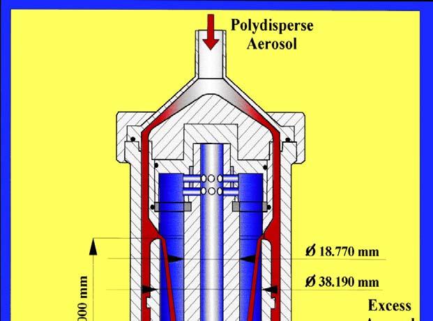
18 Experimental Setup Chamber Cover P2 Main Chamber v P = Q A P P 1 2 Turbo Axial jet injector Q: volumetric flow Pump Opposing jet injector Particle injection Pump P1 Kim, J.H. et al., J. Vacuum Sci. Technol. A24(2): (2005) 18
19 Thermophoresis Test Set Up No Gradient With Gradient T = 0 K/cm Quiescent Zone T = 10 K/cm Quiescent Zone Gas Flow Gas Flow Experimental cases: P: 100 mtorr, 50 mtorr T: d p : v i : 0 K/cm, -10 K/cm 125 nm, 220 nm (on wafers) 70 nm, 100 nm (on masks) below, at, or above critical speed Gap: 1, 2 or 3 cm Kim, J.H. et al., J. Vacuum Sci. Technol. B24(3): (2005) 19

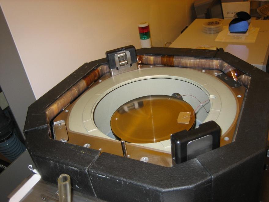
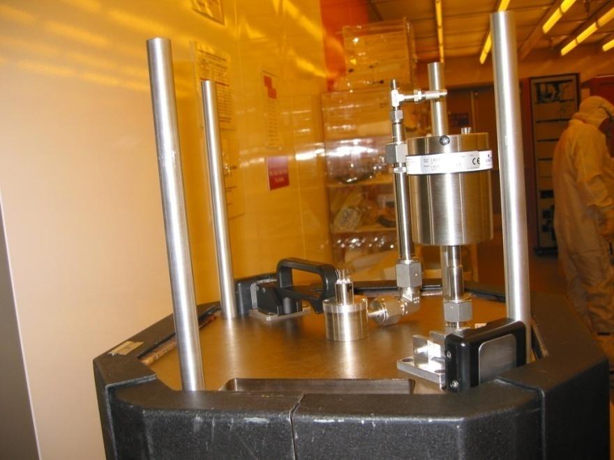
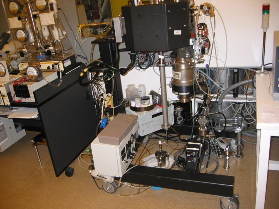
20 Vacuum chamber 20
21 Thermophoresis at 100 mtorr, 3 cm Gap 100 mtorr d p = 125 nm d p = 220 nm v p = 31 m/s for 125 nm v p = 18 m/s for 220 nm No particles deposited as predicted by the analytical model. Kim, J.H. et al., J. Vacuum Sci. Technol. B24(3): (2005) 21
22 Thermophoresis at 100 mtorr, 1 cm Gap 100 mtorr v p = 31 m/s for 125 nm v p = 18 m/s for 220 nm d p = 125 nm d p = 220 nm Particles deposited as predicted. Evidence of bouncing and diffusion is seen. Kim, J.H. et al., J. Vacuum Sci. Technol. B24(3): (2005) 22
23 Thermophoresis at 100 mtorr, 2 cm Gap 100 mtorr v p = 31 m/s for 125 nm v p = 18 m/s for 220 nm d p = 125 nm d p = 220 nm Thermophoresis improves protection. Kim, J.H. et al., J. Vacuum Sci. Technol. B24(3): (2005) 23

24 Real Mask Deposition 50 mtorr, 70 nm, 0 K/cm Main Chamber p = 50 mtorr Flow rate = lpm Particle C = 600 p/cc Testing time: 40 min Particle speed: 24.2 m/s Critical speed: m/s Pre-scan Post-scan Particles deposited in confined area 70 nm particles mainly correspond to 10 pixel particles. About pixel particles are added. 24

25 Real Mask Deposition 50 mtorr, 70 nm, 0 K/cm Main Chamber p = 50 mtorr Flow rate = lpm Particle C = 330 p/cc Testing time: 40 min Particle speed: 9.0 m/s Critical speed: m/s Pre-scan Post-scan Enhanced diffusion obvious About pixel particles are added near the center. These particles first stop then diffuse to the mask surface. Small particles show strong diffusion effect. 25
26 Simulations at 50 mtorr 125 nm, 1 cm Gap, v i = 6.5 m/s [m/s] - T = 0 K/cm - T = 10 K/cm Many particles deposited (some by diffusion) No particles deposited Thermophoresis overcomes diffusion. 26
27 Outline Protection Schemes for EUVL Masks Carriers at Atmospheric Pressure Scanners at below 100 mtorr Nanoparticle Metrology and AMC Issues Standardization of Nanoparticles Mask Deposition and AMC Issues 27

28 New NIST Nanoparticle Standards: 60 nm and 100 nm SRM 28

29 Nanometer Differential Mobility Analyzer (Nano-DMA) 29
30 Outline Protection Schemes for EUVL Masks Carriers at Atmospheric Pressure Scanners at below 100 mtorr Nanoparticle Metrology and AMC Issues Standardization of Nanoparticles Mask Deposition and AMC Issues 30

 100 nm PSL particle.")
31 Haze Observed under Atmospheric and Vacuum Conditions 50nm SiO 2. Target deposition area: 1inch spot size at the center. Testing time: 2 min. (Atmospheric Pressure) 100 nm PSL particle. (Main Chamber p = 50 mtorr). Testing time: 1.5 hours 31
32 Airborne Molecular Contaminants (AMCs) Classification of AMCs Acids HF H 2 SO 4 HCl HNO 3 H 3 PO 4 HBr Condensable No Classes H 2 O 2 O 3 IPA Acetone Bases AMINE NH 3 NMP HMDS Dopants DOP DBP DEP Siloxanes BHT B 2 H 6 BF 3 AsH 3 TCEP TEP TPP SEMI Standard F21-95,
33 High speed injection, 100 nm, 10 K/cm (Vacuum) Main Chamber p = 50 mtorr Flow rate = lpm Particle C = p/cc Testing time: 50 min Particle speed: 11.3 m/s Critical speed: m/s 100 nm particles mainly correspond to 20 pixel particles. About pixel particles are added. 33
 Known material Known number of particles NIST-traceable particle size Controlled deposition spot")
34 Controlled Particle Deposition on Mask Blanks Deposition Plan (~ 2000 particles) Detection of Particles on a Quartz Mask PSL # ~ 2010 PSL # ~ 2060 PSL # ~ 2000 PSL # ~ 1930 SiO2 # ~ 1950 SiO2 # ~ 1820 SiO2 # ~ 2060 SiO2 # ~ 2010 SiO2 # ~ 1980 Mask Scan Area (140 mm x 140 mm) Known material Known number of particles NIST-traceable particle size Controlled deposition spot size 34
35 Summary Experimental methods and models have been developed to evaluate protection schemes for masks in carrier or vacuum tools. New carriers with tapered standoff generates almost no particles during shipping. Face-down mounting and cover plate are very effective in protection. Thermophoresis is most helpful to protect against particles driven by diffusion. Method has been developed to deposit standard nanoparticles for inspection tool calibration. Method has been developed to avoid haze formation caused by AMC. 35

36 Acknowledgement Intel Corporation -- Kevin Orvek, Peiyang Yan and Ted Liang Sematech -- Long He H. Fissan, U. of Duisburg-Essen C. Asbach, T. van der Zwaag, T. Engelke, IUTA, Duisburg J. Wang, J.H. Kim, C. Qi, Post-docs S.J. Yook, Y. Liu, Ph.D. students 36
Nanoparticle Contamination Control and Metrology for the EUVL Systems
 Nanoparticle Contamination Control and Metrology for the EUVL Systems David Y. H. Pui Distinguished McKnight University Professor Mechanical Engineering Department University of Minnesota Jing Wang Assistant
Nanoparticle/AMC Contamination Control and Metrology for the EUVL Systems
 Nanoparticle/AMC Contamination Control and Metrology for the EUVL Systems David Y. H. Pui Distinguished McKnight University Professor Director of the Particle Technology Laboratory Mechanical Engineering
Defects Panel Discussion
 Defects Panel Discussion David Y. H. Pui Distinguished McKnight University Professor LM Fingerson/TSI Inc Chair in Mechanical Engineering Director of the Particle Technology Laboratory University of Minnesota
DMA Size-Selection and Electrostatic Deposition of Particle Size Standards Down to 10nm
 DMA Size-Selection and Electrostatic Deposition of Particle Size Standards Down to 10nm Ben Hunt, William Dick, Zeeshan Syedain MSP Corporation 1 AAAR 2013 3IM.4 Presentation Outline Particle Deposition
STANDARD: SPECIFICATION FOR PROTECTIVE ENCLOSURE AND CARRIER SYSTEMS USED TO TRANSPORT AND STORE ( INCH EUV RETICLES
 Entegris Edit -SEMI Draft Document (10-11-2006 Revision) NEW STANDARD: SPECIFICATION FOR PROTECTIVE ENCLOSURE AND CARRIER SYSTEMS USED TO TRANSPORT AND STORE 6 INCH EUV RETICLES This specification draft
Fiducial Marks for EUV mask blanks. Jan-Peter Urbach, James Folta, Cindy Larson, P.A. Kearney, and Thomas White
 Fiducial Marks for EUV mask blanks Jan-Peter Urbach, James Folta, Cindy Larson, P.A. Kearney, and Thomas White Fiducial marks are laser scribed on 200 mm wafers to enable defect registration on metrology
Experimental Study of Particle Deposition on Semiconductor Wafers
 Aerosol Science and Technology ISSN: 0278-6826 (Print) 1521-7388 (Online) Journal homepage: http://www.tandfonline.com/loi/uast20 Experimental Study of Particle Deposition on Semiconductor Wafers David
Mobility-Based Particle Size Classification and Detection down to 2nm Theory to Practice
 Mobility-Based Particle Size Classification and Detection down to 2nm Theory to Practice Robert C. Anderson Presented at SEMATECH November 12, 2012 Current and Future Defectively Issues from Components
A short pulsed laser cleaning system for EUVL tool
 A short pulsed laser cleaning system for EUVL tool Masami Yonekawa, Hisashi Namba and Tatsuya Hayashi Nanotechnology & Advanced System Research Laboratories, Canon inc. 23-10, Kiyohara-Kogyodanchi, Utsunomiya-shi,
Model 2300XP PSL & Process-Particle Wafer Deposition System
 Model 2300XP PSL & Process-Particle Wafer Deposition System Deposit PSL spheres on wafers to create NISTtraceable PSL size standards for - calibrating wafer inspection systems - providing fab-wide and
Mat. Res. Soc. Symp. Proc. Vol Materials Research Society
 Mat. Res. Soc. Symp. Proc. Vol. 738 2003 Materials Research Society G7.26.1 Determination of the Plastic Behavior of Low Thermal Expansion Glass at the Nanometer Scale Richard Tejeda, 1 Roxann Engelstad,
ELECTROSTATIC CLASSIFIER MODEL 3082
 ELECTROSTATIC CLASSIFIER MODEL 3082 THESE INSTRUMENTS HAVE BEEN USED IN A BROAD VARIETY OF RESEARCH AND HAVE EARNED A WELL-DESERVED REPUTATION FOR BEING HIGHLY RELIABLE AND EXTREMELY VERSATILE. UNDERSTANDING,
Recent Advances and Challenges in Nanoparticle Monitoring for the Semiconductor Industry. December 12, 2013
 Recent Advances and Challenges in Nanoparticle Monitoring for the Semiconductor Industry December 12, 2013 Agenda Introduction Wafer Environment Nano-Contamination Requirements State-of-the-Art Monitoring
ITRS, SEMI and ASTM Guidelines for Semiconductor Ultrapure Water (UPW) Production and the Consequences for UPW Particle Metrology
 Production and the Consequences for UPW Particle Metrology") ITRS, SEMI and ASTM Guidelines for Semiconductor Ultrapure Water (UPW) Production and the Consequences for UPW Particle Metrology David Blackford, Ph.D. Fluid Measurement Technologies, Inc. St. Paul, Minnesota
ITRS, SEMI and ASTM Guidelines for Semiconductor Ultrapure Water (UPW) Production and the Consequences for UPW Particle Metrology David Blackford, Ph.D. Fluid Measurement Technologies, Inc. St. Paul, Minnesota
EUVL Readiness for High Volume Manufacturing
 EUVL Readiness for High Volume Manufacturing Britt Turkot Intel Corporation Outline Exposure Tool Progress Power Availability Intel demo results Reticle Defectivity Pellicle Materials Conclusion 2 Source
Analysis of carbon contamination on EUV mask using CSM/ ICS
 Analysis of carbon contamination on EUV mask using CSM/ ICS Jae Uk Lee 1, Chang Young Jeong 1, Sangsul Lee 1, Jong Gul Doh 1,, Dong Geun Lee 2, Seong-Sue Kim 2, Han-Ku Cho 2, Seung-yu Rah 3 and Jinho Ahn
Overview of EUV Lithography and EUV Optics Contamination
 Accelerating the next technology revolution Overview of EUV Lithography and EUV Optics Contamination Andrea Wüest NIST Contamination WS Gaithersburg, MD June 2, 2009 Copyright 2008 SEMATECH, Inc. SEMATECH,
UNIT 3. By: Ajay Kumar Gautam Asst. Prof. Dev Bhoomi Institute of Technology & Engineering, Dehradun
 UNIT 3 By: Ajay Kumar Gautam Asst. Prof. Dev Bhoomi Institute of Technology & Engineering, Dehradun 1 Syllabus Lithography: photolithography and pattern transfer, Optical and non optical lithography, electron,
Measurement of EUV scattering from Mo/Si multilayer mirrors
 Measurement of EUV scattering from Mo/Si multilayer mirrors N. Kandaka, T. Kobayashi, T. Komiya, M. Shiraishi, T. Oshino and K. Murakami Nikon Corp. 3 rd EUVL Symposium Nov. 2-4 2004 (Miyazaki, JAPAN)
The Characterization of Nanoparticle Element Oxide Slurries Used in Chemical-Mechanical Planarization by Single Particle ICP-MS
 A P P L I C AT I O N N O T E ICP - Mass Spectrometry Authors: Lee Davidowski Chady Stephan PerkinElmer, Inc. Shelton, CT The Characterization of Nanoparticle Element Oxide Slurries Used in Chemical-Mechanical
DEPOSITION OF THIN TiO 2 FILMS BY DC MAGNETRON SPUTTERING METHOD
 Chapter 4 DEPOSITION OF THIN TiO 2 FILMS BY DC MAGNETRON SPUTTERING METHOD 4.1 INTRODUCTION Sputter deposition process is another old technique being used in modern semiconductor industries. Sputtering
Industrial Applications of Ultrafast Lasers: From Photomask Repair to Device Physics
 Industrial Applications of Ultrafast Lasers: From Photomask Repair to Device Physics Richard Haight IBM TJ Watson Research Center PO Box 218 Yorktown Hts., NY 10598 Collaborators Al Wagner Pete Longo Daeyoung
Introduction to Photolithography
 http://www.ichaus.de/news/72 Introduction to Photolithography Photolithography The following slides present an outline of the process by which integrated circuits are made, of which photolithography is
Visualization of Xe and Sn Atoms Generated from Laser-Produced Plasma for EUV Light Source
 3rd International EUVL Symposium NOVEMBER 1-4, 2004 Miyazaki, Japan Visualization of Xe and Sn Atoms Generated from Laser-Produced Plasma for EUV Light Source H. Tanaka, A. Matsumoto, K. Akinaga, A. Takahashi
The Removal of Nanoparticles from Nanotrenches Using Megasonics
 NSF Center for Micro and Nanoscale Contamination Control The Removal of Nanoparticles from Nanotrenches Using Megasonics Pegah Karimi 1, Tae Hoon Kim 1, Ahmed A. Busnaina 1 and Jin Goo Park 2 1 NSF Center
Chapter 5: Nanoparticle Production from Cathode Sputtering. in High-Pressure Microhollow Cathode and Arc Discharges
 96 Chapter 5: Nanoparticle Production from Cathode Sputtering in High-Pressure Microhollow Cathode and Arc Discharges 5.1. Introduction Sputtering is a fundamental aspect of plasma operation and has been
Calibration checks of particle counter using primary and other techniques at the laboratory level
 Calibration checks of particle counter using primary and other techniques at the laboratory level Shankar G. Aggarwal, Ph.D. CSIR-National Physical Laboratory, New Delhi-110 012, India @ Particulate Workshop
E152 Standard Revision: EUV-pod Reticle Carrier
 E152 Standard Revision: EUV-pod Reticle Carrier February 27, 2011, San Jose EUV Reticle Handling TF Co-chairs/Key Contributors: Long He (Intel), David Halbmaier (Entegris), John Lystad (Entegris), John
Wavelength-Specific Reflections A Decade of EUV Mask Inspection Research
 Wavelength-Specific Reflections A Decade of EUV Mask Inspection Research Kenneth Goldberg, Iacopo Mochi Lawrence Berkeley National Laboratory 1 The main things you need to know EUV reticle Samsung 2007
Accelerated Neutral Atom Beam Processing of Ultra-thin Membranes to Enhance EUV Transmittance. February 22, 2015
 Accelerated Neutral Atom Beam Processing of Ultra-thin Membranes to Enhance EUV Transmittance February 22, 2015 1 Participation / Contacts Exogenesis Corporation, ANAB Technology Sean Kirkpatrick, Son
Actinic review of EUV masks: First results from the AIMS EUV system integration
 Invited Paper Actinic review of EUV masks: First results from the AIMS EUV system integration Markus R. Weiss* a, Dirk Hellweg a, Jan Hendrik Peters b, Sascha Perlitz b, Anthony Garetto b, Michael Goldstein
Figure 2. Size distribution and concentration of a cocktail of PSL particles measured by three different sizing instruments.
 Nano-Particle Standards and their use for Particle Counter Calibration and Particle Deposition Studies by David Blackford Ph.D. Kanomax FMT, Inc. Gary Van Schooneveld CT Associates, Inc. A particle standard
A Study to Measure the Chemical Characteristics of Particle Emissions from Biomass Burning Stoves
 A Study to Measure the Chemical Characteristics of Particle Emissions from Biomass Burning Stoves End of Summer Workshop, 2006 Dabrina Dutcher School of Public Health and Department of Mechanical Engineering
Vapor-Phase Cutting of Carbon Nanotubes Using a Nanomanipulator Platform
 Vapor-Phase Cutting of Carbon Nanotubes Using a Nanomanipulator Platform MS&T 10, October 18, 2010 Vladimir Mancevski, President and CTO, Xidex Corporation Philip D. Rack, Professor, The University of
Lithography. The Crystal Growth and Reticle Degradation Exposé. Reticle Surface Contaminants and Their Relationship to Sub-pellicle Particle Formation
 Lithography R E T I C L E The Crystal Growth and Reticle Degradation Exposé Reticle Surface Contaminants and Their Relationship to Sub-pellicle Particle Formation Brian J. Grenon, Grenon Consulting, Incorporated
Chapter 3 Engineering Science for Microsystems Design and Fabrication
 Lectures on MEMS and MICROSYSTEMS DESIGN and MANUFACTURE Chapter 3 Engineering Science for Microsystems Design and Fabrication In this Chapter, we will present overviews of the principles of physical and
Effects of Size, Humidity, and Aging on Particle Removal
 LEVITRONIX Ultrapure Fluid Handling and Wafer Cleaning Conference 2009 February 10, 2009 Effects of Size, Humidity, and Aging on Particle Removal Jin-Goo Park Feb. 10, 2009 Department t of Materials Engineering,
SCALING OF THE ADHESION BETWEEN PARTICLES AND SURFACES FROM MICRON-SCALE TO THE NANOMETER SCALE FOR PHOTOMASK CLEANING APPLICATIONS
 SCALING OF THE ADHESION BETWEEN PARTICLES AND SURFACES FROM MICRON-SCALE TO THE NANOMETER SCALE FOR PHOTOMASK CLEANING APPLICATIONS Gautam Kumar, Shanna Smith, Florence Eschbach, Arun Ramamoorthy, Michael
Supplementary Materials for
 www.sciencemag.org/content/351/6271/361/suppl/dc1 Supplementary Materials for Active sites of nitrogen-doped carbon materials for oxygen reduction reaction clarified using model catalysts Donghui Guo,
Jianfei Peng et al. Correspondence to: Jianfei Peng Min Hu and Renyi Zhang
 Supplement of Atmos. Chem. Phys., 17, 10333 10348, 2017 https://doi.org/10.5194/acp-17-10333-2017-supplement Author(s) 2017. This work is distributed under the Creative Commons Attribution 3.0 License.
Analysis of Data from the 2009 SOOT Experiment
 Analysis of Data from the 2009 SOOT Experiment Renyi Zhang Department of Atmospheric Sciences and Department of Chemistry Center for Atmospheric Chemistry and the Environment Texas A&M University College
Processing of Semiconducting Materials Prof. Pallab Banerji Department of Metallurgy and Material Science Indian Institute of Technology, Kharagpur
 Processing of Semiconducting Materials Prof. Pallab Banerji Department of Metallurgy and Material Science Indian Institute of Technology, Kharagpur Lecture - 9 Diffusion and Ion Implantation III In my
Thermal Expansion property and Surface Finish capability of CLEARCERAM -Z series for EUVL Photomask Substrate Application
 Thermal Expansion property and Surface Finish capability of CLEARCERAM -Z series for EUVL Photomask Substrate Application Kousuke Nakajima, Toshihide Nakajima, Yoshiyuki Owari OHARA Incorporated 3 rd International
Ion Implantation. alternative to diffusion for the introduction of dopants essentially a physical process, rather than chemical advantages:
 Ion Implantation alternative to diffusion for the introduction of dopants essentially a physical process, rather than chemical advantages: mass separation allows wide varies of dopants dose control: diffusion
Tilted ion implantation as a cost-efficient sublithographic
 Tilted ion implantation as a cost-efficient sublithographic patterning technique Sang Wan Kim 1,a), Peng Zheng 1, Kimihiko Kato 1, Leonard Rubin 2, Tsu-Jae King Liu 1 1 Department of Electrical Engineering
P R O D U C T. he Model 3800 Aerosol Time-of-Flight Mass Spectrometer. Determines size and chemical composition of single particles
 P R O D U C T I N F O R M A T I O N Model 3800 Aerosol Time-of-Flight Mass Spectrometer TSI Incorporated s Aerosol Time-of-Flight Mass Spectrometer (ATOFMS) is the first commercial instrument to offer
Characterization of particle contamination in process steps during plasma-enhanced chemical vapor deposition operation
 Aerosol Science 34 (2003) 923 936 www.elsevier.com/locate/jaerosci Characterization of particle contamination in process steps during plasma-enhanced chemical vapor deposition operation Heru Setyawan,
Airborne Molecular Contamination Control Technology in the Semiconductor Industry
 G u e s t F o r u m Guest Forum Airborne Molecular Contamination Control Technology in the Semiconductor Industry Iwao Yoshizawa, Akifumi Kagawa Dan-Takuma Technologies Inc. will begin to sell a continuous
After Development Inspection (ADI) Studies of Photo Resist Defectivity of an Advanced Memory Device
 Studies of Photo Resist Defectivity of an Advanced Memory Device") After Development Inspection (ADI) Studies of Photo Resist Defectivity of an Advanced Memory Device Hyung-Seop Kim, Yong Min Cho, Byoung-Ho Lee Semiconductor R&D Center, Device Solution Business, Samsung
After Development Inspection (ADI) Studies of Photo Resist Defectivity of an Advanced Memory Device Hyung-Seop Kim, Yong Min Cho, Byoung-Ho Lee Semiconductor R&D Center, Device Solution Business, Samsung
Acoustic Streaming Effects in Megasonic Cleaning of EUV Photomasks: A continuum model.
 Acoustic Streaming Effects in Megasonic Cleaning of EUV Photomasks: A continuum model. Vivek Kapila a, Pierre A. Deymier a, Hrishikesh Shende a, Viraj Pandit b, Srini Raghavan a and Florence O. Eschbach
Section 3: Etching. Jaeger Chapter 2 Reader
 Section 3: Etching Jaeger Chapter 2 Reader Etch rate Etch Process - Figures of Merit Etch rate uniformity Selectivity Anisotropy d m Bias and anisotropy etching mask h f substrate d f d m substrate d f
EUV Lithography Status and Key Challenges for HVM Implementation
 EUV Lithography Status and Key Challenges for HVM Implementation Sam Intel Corporation Moore s Law at Intel 10 Feature Size (um) 100 Cell Area (sq um) 1 10 0.5x every 2 years 0.1 1 0.01 1970 1980 1990
Fundamentals of Particle Counting
 Fundamentals of Particle Counting 1 Particle Counting: Remains the most significant technique for determining the cleanliness level of a fluid Useful as a tool for qualification and monitoring cleanroom
ASML Approach to Euv Reticle Handling
 ASML Approach to Euv Reticle Handling Mask Workshop Antwerp Henk Meijer 3-October-2003 / Slide 1 Presentation Agenda Unique features of EUV reticles Contamination
Defect management and control. Tsuyoshi Moriya, PhD Senior Manager Tokyo Electron Limited
 Defect management and control Tsuyoshi Moriya, PhD Senior Manager Tokyo Electron Limited Background Case study: A maintainer has good hands Only he achieved good yield for every maintenance But... He could
Ablation Dynamics of Tin Micro-Droplet Target for LPP-based EUV light Source
 1 Ablation Dynamics of Tin Micro-Droplet Target for LPP-based EUV light Source D. Nakamura, T. Akiyama, K. Tamaru, A. Takahashi* and T. Okada Graduate School of Information Science and Electrical Engineering,
CURRENT STATUS OF NANOIMPRINT LITHOGRAPHY DEVELOPMENT IN CNMM
 U.S. -KOREA Forums on Nanotechnology 1 CURRENT STATUS OF NANOIMPRINT LITHOGRAPHY DEVELOPMENT IN CNMM February 17 th 2005 Eung-Sug Lee,Jun-Ho Jeong Korea Institute of Machinery & Materials U.S. -KOREA Forums
Critical Dimension Uniformity using Reticle Inspection Tool
 Critical Dimension Uniformity using Reticle Inspection Tool b Mark Wylie, b Trent Hutchinson, b Gang Pan, b Thomas Vavul, b John Miller, b Aditya Dayal, b Carl Hess a Mike Green, a Shad Hedges, a Dan Chalom,
We published the text from the next page.
 Title:Shedding light on EUV mask inspection Authors:Kazunori Seki, Karen Badger, Emily Gallagher, Toshio Konishi, Gregory McIntyre Publisher:Photomask Japan 2012(SPIE) Citation:Kazunori Seki, Karen Badger,
Optical Proximity Correction
 Optical Proximity Correction Mask Wafer *Auxiliary features added on mask 1 Overlay Errors + + alignment mask wafer + + photomask plate Alignment marks from previous masking level 2 (1) Thermal run-in/run-out
Fundamentals of Mass Spectrometry. Fundamentals of Mass Spectrometry. Learning Objective. Proteomics
 Mass spectrometry (MS) is the technique for protein identification and analysis by production of charged molecular species in vacuum, and their separation by magnetic and electric fields based on mass
CENG 501 Examination Problem: Estimation of Viscosity with a Falling - Cylinder Viscometer
 CENG 501 Examination Problem: Estimation of Viscosity with a Falling - Cylinder Viscometer You are assigned to design a fallingcylinder viscometer to measure the viscosity of Newtonian liquids. A schematic
XPS & Scanning Auger Principles & Examples
 XPS & Scanning Auger Principles & Examples Shared Research Facilities Lunch Talk Contact info: dhu Pujari & Han Zuilhof Lab of rganic Chemistry Wageningen University E-mail: dharam.pujari@wur.nl Han.Zuilhof@wur.nl
The study for image placement repeatability of EUV mask on the flat chuck
 The study for image placement repeatability of EUV mask on the flat chuck Shusuke Yoshitake, Hitoshi Sunaoshi, Shuichi Tamamushi, Soichiro Mitsui 1, Munehiro Ogasawara 1, Takeyuki Yamada 2, Tsutomu Shoki
Rapid Measurements of Aerosol Size Distributions Using a Fast Integrated Mobility Spectrometer (FIMS)
") Rapid Measurements of Aerosol Size Distributions Using a Fast Integrated Mobility Spectrometer (FIMS) Jason Olfert, Brookhaven National Laboratory Jian Wang, Brookhaven National Laboratory Measurement
Rapid Measurements of Aerosol Size Distributions Using a Fast Integrated Mobility Spectrometer (FIMS) Jason Olfert, Brookhaven National Laboratory Jian Wang, Brookhaven National Laboratory Measurement
UNIVERSITY OF CALIFORNIA College of Engineering Department of Electrical Engineering and Computer Sciences. Fall Exam 1
 UNIVERSITY OF CALIFORNIA College of Engineering Department of Electrical Engineering and Computer Sciences EECS 143 Fall 2008 Exam 1 Professor Ali Javey Answer Key Name: SID: 1337 Closed book. One sheet
Forming Gradient Multilayer (GML) Nano Films for Photovoltaic and Energy Storage Applications
 Nano Films for Photovoltaic and Energy Storage Applications") Forming Gradient Multilayer (GML) Nano Films for Photovoltaic and Energy Storage Applications ABSTRACT Boris Gilman and Igor Altman Coolsol R&C, Mountain View CA For successful implementation of the nanomaterial-based
Forming Gradient Multilayer (GML) Nano Films for Photovoltaic and Energy Storage Applications ABSTRACT Boris Gilman and Igor Altman Coolsol R&C, Mountain View CA For successful implementation of the nanomaterial-based
PARTICLE CONTROL AT 100 nm NODE STATUS WORKSHOP: PARTICLES IN PLASMAS
 PARTICLE CONTROL AT 100 nm NODE STATUS WORKSHOP: PARTICLES IN PLASMAS Mark J. Kushner University of Illinois Department of Electrical and Computer Engineering Urbana, IL 61801 mjk@uiuc.edu December 1998
UC San Diego EUV Lithography Group Progress Report
 University of California, San Diego UCSD-CER-10-02 UC San Diego EUV Lithography Group Progress Report M. S. Tillack, Y. Tao, F. Najmabadi, L. Carlson, S. Yuspeh, R. Burdt, A. Farkas, N. Shaikh, N. Amin,
6.5 Optical-Coating-Deposition Technologies
 92 Chapter 6 6.5 Optical-Coating-Deposition Technologies The coating process takes place in an evaporation chamber with a fully controlled system for the specified requirements. Typical systems are depicted
IEUVI Mask Technical Working Group
 IEUVI Mask Technical Working Group Proposed changes P37/P38/P40 SEMI standards Thursday, Feb 28, 2008 / Slide 1 Introduction All of the recommendations are driven by the
PHOTOELECTRON SPECTROSCOPY IN AIR (PESA)
") PHOTOELECTRON SPECTROSCOPY IN AIR (PESA) LEADERS IN GAS DETECTION Since 1977 Model AC-3 Features: Atmospheric pressure operation (unique in the world) Estimate work function, ionization potential, density
PHOTOELECTRON SPECTROSCOPY IN AIR (PESA) LEADERS IN GAS DETECTION Since 1977 Model AC-3 Features: Atmospheric pressure operation (unique in the world) Estimate work function, ionization potential, density
Aspects of Single Wafer Cleans Processing and Tools
 Aspects of Single Wafer Cleans Processing and Tools Steven Verhaverbeke, Santa Clara, CA Date: June 16th, 2011 Contents 2 Generalities on Particles Generalities on particles in a chamber environment gas
Scanning Tunneling Microscopy
 Scanning Tunneling Microscopy Scanning Direction References: Classical Tunneling Quantum Mechanics Tunneling current Tunneling current I t I t (V/d)exp(-Aφ 1/2 d) A = 1.025 (ev) -1/2 Å -1 I t = 10 pa~10na
CHAPTER A2 LASER DESORPTION IONIZATION AND MALDI
 Back to Basics Section A: Ionization Processes CHAPTER A2 LASER DESORPTION IONIZATION AND MALDI TABLE OF CONTENTS Quick Guide...27 Summary...29 The Ionization Process...31 Other Considerations on Laser
Overview of the Particle Size Magnifier (PSM)
") Overview of the Particle Size Magnifier (PSM) Joonas Vanhanen CTO, Airmodus Ltd. joonas.vanhanen@airmodus.com Airmodus Ltd. It s the small things that count Founded in 2010 A spin-off from the University
Overview of the Particle Size Magnifier (PSM) Joonas Vanhanen CTO, Airmodus Ltd. joonas.vanhanen@airmodus.com Airmodus Ltd. It s the small things that count Founded in 2010 A spin-off from the University
VACUUM SUPPORT FOR A LARGE INTERFEROMETRIC REFERENCE SURFACE
 VACUUM SUPPORT FOR A LARGE INTERFEROMETRIC REFERENCE SURFACE Masaki Hosoda, Robert E. Parks, and James H. Burge College of Optical Sciences University of Arizona Tucson, Arizona 85721 OVERVIEW This paper
COPLEY S C I E N T I F I C. A multi-function aerosol system with aerosol generation, classification and monitoring capabilities for:
 A multi-function aerosol system with aerosol generation, classification and monitoring capabilities for: generating monodisperse aerosol by mobility classification with automatic concentration detection
Extrel Application Note
 Extrel Application Note Real-Time Plasma Monitoring and Detection of Trace H 2 O and HF Species in an Argon Based Plasma Jian Wei, 575 Epsilon Drive, Pittsburgh, PA 15238. (Presented at the 191st Electrochemical
Effective testing for wafer reject minimization by terahertz analysis and sub-surface imaging
 Effective testing for wafer reject minimization by terahertz analysis and sub-surface imaging Anis Rahman and Aunik K. Rahman Applied Research & Photonics 470 Friendship Road, Suite 10 Harrisburg, PA 17111,
Development status of back-end process for UV-NIL template fabrication
 Development status of back-end process for UV-NIL template fabrication Yuichi Inazuki, Kimio Itoh, Sho Hatakeyama, Kouichirou Kojima, Masaaki Kurihara, Yasutaka Morikawa, Hiroshi Mohri and Naoya Hayashi
Optical Measurements of Critical Dimensions at Several Stages of the Mask Fabrication Process
 Optical Measurements of Critical Dimensions at Several Stages of the Mask Fabrication Process John C. Lam, Alexander Gray n&k Technology, Inc., Santa Clara, CA ABSTRACT Critical dimension (CD) metrology
Micro Chemical Vapor Deposition System: Design and Verification
 Micro Chemical Vapor Deposition System: Design and Verification Q. Zhou and L. Lin Berkeley Sensor and Actuator Center, Department of Mechanical Engineering, University of California, Berkeley 2009 IEEE
Secondary ion mass spectrometry (SIMS)
") Secondary ion mass spectrometry (SIMS) ELEC-L3211 Postgraduate Course in Micro and Nanosciences Department of Micro and Nanosciences Personal motivation and experience on SIMS Offers the possibility to
Secondary ion mass spectrometry (SIMS) ELEC-L3211 Postgraduate Course in Micro and Nanosciences Department of Micro and Nanosciences Personal motivation and experience on SIMS Offers the possibility to
Measurement of the role of secondary electrons in EUV resist exposures
 Measurement of the role of secondary electrons in EUV resist exposures June 12, 213 International Workshop on EUV Lithography Greg Denbeaux a, Justin Torok, a Ryan Del Re, a Henry Herbol, a Sanjana Das,
Current development status of Shin-Etsu EUV pellicle
 Current development status of Shin-Etsu EUV pellicle Advanced Functional Materials Research Center 1 Why Pellicle for EUV Lithography? Extensive studies on particle addition during reticle transfer have
Lecture 16 Light transmission and optical detectors
 Lecture 6 Light transmission and optical detectors Charged particle traversing through a material can generate signal in form of light via electromagnetic interactions with orbital electrons of the atoms
Generation and Evaluation of Monodisperse Sodium Chloride and Oleic Acid Nanoparticles
 Generation and Evaluation of Monodisperse Sodium Chloride and Oleic Acid Nanoparticles Tzu Ming Chen, Hung Min Chein Energy & Environment Research Laboratories, Industrial Technology Research Institute,
TRANSVERSE SPIN TRANSPORT IN GRAPHENE
 International Journal of Modern Physics B Vol. 23, Nos. 12 & 13 (2009) 2641 2646 World Scientific Publishing Company TRANSVERSE SPIN TRANSPORT IN GRAPHENE TARIQ M. G. MOHIUDDIN, A. A. ZHUKOV, D. C. ELIAS,
EUVL for HVM: Progress Update
 EUVL for HVM: Progress Update Mark Phillips Intel Corporation EUVL Workshop, Maui, Hawaii, 17 June 2015, Mark Phillips (Intel) Outline EUV source and system performance EUV/193i complementary patterning
Modelling of temperature profiles in Nd:YAG laser annealed GaAs/AlGaAs quantum well microstructures
 Modelling of temperature profiles in Nd:YG laser annealed Gas/lGas quantum well microstructures Radoslaw Stanowski Ph.D. O. Voznyy prof. J J. Dubowski 1 Outline 1. Motivation 2. Transient temperature analysis
NANO AND MICROSCALE PARTICLE REMOVAL
 NANO AND MICROSCALE PARTICLE REMOVAL Ahmed A. Busnaina William Lincoln Smith Professor and Director of the oratory Northeastern University, Boston, MA 2115-5 OUTLINE Goals and Objectives Approach Preliminary
Modeling of Ion Energy Distribution Using Time-Series Neural Network
 12th SEAS International Conference on SYSTEMS, Heralion, Greece, July 22-24, 2008 Modeling of Ion Energy Distribution Using Time-Series Neural Networ Suyeon Kim, Byungwhan Kim* Department of Electronic
EUV Lithography Towards Industrialization
 EUV Lithography Towards Industrialization Wim van der Zande, Director of Research, ASML Dublin Meeting November 2014 Slide 2 Agenda EUV benefit and status at customers Towards higher productivity Summary
Final report on DOE project number DE-FG07-99ID High Pressure Xenon Gamma-Ray Spectrometers for Field Use
 Final report on DOE project number DE-FG07-99ID13772 High Pressure Xenon Gamma-Ray Spectrometers for Field Use Principle Investigator: Glenn K. Knoll Co-investigator: David K. Wehe, Zhong He, University
Copyright 1996, by the author(s). All rights reserved.
. All rights reserved.") Copyright 1996, by the author(s). All rights reserved. Permission to make digital or hard copies of all or part of this work for personal or classroom use is granted without fee provided that copies are
Copyright 1996, by the author(s). All rights reserved. Permission to make digital or hard copies of all or part of this work for personal or classroom use is granted without fee provided that copies are
Carbon Nanotube Thin-Films & Nanoparticle Assembly
 Nanodevices using Nanomaterials : Carbon Nanotube Thin-Films & Nanoparticle Assembly Seung-Beck Lee Division of Electronics and Computer Engineering & Department of Nanotechnology, Hanyang University,
ETCHING Chapter 10. Mask. Photoresist
 ETCHING Chapter 10 Mask Light Deposited Substrate Photoresist Etch mask deposition Photoresist application Exposure Development Etching Resist removal Etching of thin films and sometimes the silicon substrate
FINAL REPORT. DOE Grant DE-FG03-87ER13727
 FINAL REPORT DOE Grant DE-FG03-87ER13727 Dynamics of Electronegative Plasmas for Materials Processing Allan J. Lichtenberg and Michael A. Lieberman Department of Electrical Engineering and Computer Sciences
KEYWORDS plasma enhanced chemical vapor deposition, dusty plasma, particulate contamination, film growth rate
 Evaluation of Dust Particle Properties and Particulate Contamination in a PECVD Reactor by Visualization Measurements On-line Number 474 Yutaka Hayashi, Manabu Shimada and Kikuo Okuyama Department of Chemical