May the Force be with you: High-speed Atomic Force Microscopes for Synchrotron Sample Holders Luca Costa
|
|
|
- Louisa Foster
- 5 years ago
- Views:
Transcription

1 May the Force be with you: High-speed Atomic Force Microscopes for Synchrotron Sample Holders Luca Costa ESRF, The European Synchrotron 71 Rue des Martyrs, Grenoble, France
 Coupling")


2 EXP DIV - THE SURFACE SCIENCE LABORATORY ATOMIC FORCE MICROSCOPY (AFM) Coupling X-Rays and AFM in-situ in beamlines Provide AFM expertise to the ESRF users Asylum Research CYPHER Asylum Research MFP-3D Digital Instruments DIMENSION 3100 Page 2


3 ATOMIC FORCE MICROSCOPY Stiffness k Mass m ω = (k/m) Page 3


4 AFM: MORPHOLOGY AND INTERACTION FORCE graphene nanoparticles Z polymers microelectronics Interaction force mica Interaction Force Biology and soft materials Mechanics Chemistry Biology Page 4
5 OUTLINE Introduction to AFM High-Speed scanning probe microscopies for beamlines Grazing incidence Normal incidence Results at ID03, ID13 and ID17 Page 5

6 MOTIVATION - Follow dynamics in biology, Chemistry and radiation damage at nanoscale Myosin walking on an actin filament - Alignment between X-Ray nanofocus and nanostructures - Apply controlled Forces on the sample Page 6
7 WHERE DO WE COME FROM, WHERE DO WE GO -1- ANY CANTILEVERS CAN BE MOUNTED ON THE AFMs AFM in liquids In physiological conditions In ambient conditions Biology Electrochemistry Spectroscopy EFM MFM PFM -2- SPECIFIC X-RAY TECHNIQUE (BLs) CUSTOM X-AFM (weight, dimensions, space for scattered beam, etc.) Page 7

 Reflectivity")
 SAXS WAXS Page 8")
8 HIGH SPEED ATOMIC FORCE MICROSCOPY GRAZING INCIDENCE HS-X-AFM (ID03) Reflectivity GISAXS GIXD NORMAL INCIDENCE HS-X-AFM (ID13) SAXS WAXS Page 8
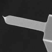

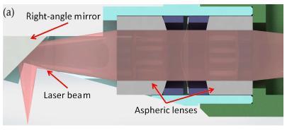

9 FAST CANTILEVERS DIMENSIONS: 9 x 2 x 0.1 μm 2 μm Need of custom-made efficient optics Page 9

")

10 FAST SCANNERS GRAZING INCIDENCE HS-X-AFM (ID03) NORMAL INCIDENCE HS-X-AFM (nano-hutch ID13) Page 10
11 OUTLINE Introduction to AFM High-Speed scanning probe microscopies for beamlines Grazing incidence Normal incidence Results at ID03, ID13 and ID17 Page 11


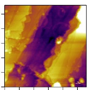
12 ID03 RADIATION DAMAGE ON MODEL MEMBRANES GRAZING INCIDENCE X-AFM DPPC Page 12


13 ID03 PHASE TRANSITION OF MODEL MEMBRANES Phase transition of DPPC GEL phase GEL and Liquid phase GEL LIQUID GEL Page 13


")

14 ID13 TESTS NORMAL INCIDENCE HS-X-AFM (nano-hutch ID13) SAMPLE IN OUT AFM CHIP At BM05 Page 14
15 TIP X-RAY BEAM ALIGNEMENT Measurement of the current flowing in the tip current Page 15


16 ID17 - RADIATION DAMAGE ON LIVING CELLS Radiation damage on living cells Morphology (membrane and cytoskeleton) Elasticity Page 16


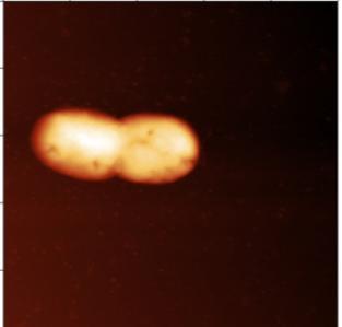
17 Cells 9L ID17 RADIATION DAMAGE ON LIVING CELLS 3 Grays 3 Grays Some parts of the cells become stiffer Page 17
18 OUR FUTURE Large beams Surface Force Apparatus and use of large probes Nano beams Use of the tip to align beam and Nanostructures Combined ptycography and fluorescence Page 18

19 ACKNOWLEDGMENTS Surface Science Lab. Fabio Comin Alain Panzarella Yohan Fuchs Christopher Chevillard ID03 Roberto Felici Francesco Carlà ID13 Manfred Burghammer Martin Rosenthal Thomas Dane ID17 Herwig Requardt Alberto Bravin Berta G. Audenis Marina I. Giannotti Fausto Sanz Mario S. Rodrigues Miguel V. Vitorino ID16 Sylvain Bohic BMF Helene Bernard Pascal Bernard Olivier Hignette Page 19

20 ID03 RADIATION DAMAGE ON MODEL MEMBRANES GRAZING INCIDENCE X-AFM DOPC Page 20
Edge Radiation IR end-station at ESRF
 X-TIP Workshop Coupling of Synchrotron Radiation IR and X-rays with Tip based Scanning Probe Microscopies 16-18 November 2005 Edge Radiation IR end-station at ESRF Jean Susini European Synchrotron Radiation
Characterization of MEMS Devices
 MEMS: Characterization Characterization of MEMS Devices Prasanna S. Gandhi Assistant Professor, Department of Mechanical Engineering, Indian Institute of Technology, Bombay, Recap Characterization of MEMS
Atomic Force Microscopy imaging and beyond
 Atomic Force Microscopy imaging and beyond Arif Mumtaz Magnetism and Magnetic Materials Group Department of Physics, QAU Coworkers: Prof. Dr. S.K.Hasanain M. Tariq Khan Alam Imaging and beyond Scanning
Scanning Probe Microscopy. Amanda MacMillan, Emmy Gebremichael, & John Shamblin Chem 243: Instrumental Analysis Dr. Robert Corn March 10, 2010
 Scanning Probe Microscopy Amanda MacMillan, Emmy Gebremichael, & John Shamblin Chem 243: Instrumental Analysis Dr. Robert Corn March 10, 2010 Scanning Probe Microscopy High-Resolution Surface Analysis
Nano-Lithography. Edited by Stefan Landis
 Nano-Lithography Edited by Stefan Landis IST^ m WILEY Table of Contents Foreword Jörge DE SOUSA NORONHA Introduction Michel BRILLOUET xi xvii Chapter 1. X-ray Lithography: Fundamentals and Applications
X-Ray Nanoimaging: Instruments And Methods II (Proceedings Of SPIE)
") X-Ray Nanoimaging: Instruments And Methods II (Proceedings Of SPIE) If you are searched for a book X-Ray Nanoimaging: Instruments and Methods II (Proceedings of SPIE) in pdf form, then you've come to the
X-Ray Nanoimaging: Instruments And Methods II (Proceedings Of SPIE) If you are searched for a book X-Ray Nanoimaging: Instruments and Methods II (Proceedings of SPIE) in pdf form, then you've come to the
NIS: what can it be used for?
 AFM @ NIS: what can it be used for? Chiara Manfredotti 011 670 8382/8388/7879 chiara.manfredotti@to.infn.it Skype: khiaram 1 AFM: block scheme In an Atomic Force Microscope (AFM) a micrometric tip attached
Atomic and molecular interactions. Scanning probe microscopy.
 Atomic and molecular interactions. Scanning probe microscopy. Balázs Kiss Nanobiotechnology and Single Molecule Research Group, Department of Biophysics and Radiation Biology 27. November 2013. 2 Atomic
Coherent X-ray diffraction for Condensed matter physics
 Coherent X-ray diffraction for Condensed matter physics Sylvain RAVY CRISTAL beamline Synchrotron SOLEIL Saint Aubin 91192 Gif-sur-Yvette France Collaborations David Le Bolloc h, (lab. physique des solides,
X-Ray Microscopy with Elemental, Chemical, and Structural Contrast
 Institut für Strukturphysik, TU Dresden, Christian Schroer (schroer@xray-lens.de) X-Ray Microscopy with Elemental, Chemical, and Structural Contrast Christian G. Schroer Institute of Structural Physics,
Julien Schmitt, postdoc in the Physical Chemistry department. Internship 2010: Study of the SAXS scattering pattern of mesoporous materials
 Before starting Julien Schmitt, postdoc in the Physical Chemistry department Internship 2010: Study of the SAXS scattering pattern of mesoporous materials PhD 2011-2014: Self-assembly mechanism of mesoporous
Chapter 12. Nanometrology. Oxford University Press All rights reserved.
 Chapter 12 Nanometrology Introduction Nanometrology is the science of measurement at the nanoscale level. Figure illustrates where nanoscale stands in relation to a meter and sub divisions of meter. Nanometrology
The most versatile AFM platform for your nanoscale microscopy needs
 The most versatile AFM platform for your nanoscale microscopy needs Atomic Force Microscopy (AFM) for nanometer resolution imaging with electrical, magnetic, thermal, and mechanical property measurement
Combining High Resolution Optical and Scanning Probe Microscopy
 Combining High Resolution Optical and Scanning Probe Microscopy Fernando Vargas WITec, Ulm, Germany www.witec.de Company Background Foundation 1997 by O. Hollricher, J. Koenen, K. Weishaupt WITec = Wissenschaftliche
Contents. What is AFM? History Basic principles and devices Operating modes Application areas Advantages and disadvantages
 Contents What is AFM? History Basic principles and devices Operating modes Application areas Advantages and disadvantages Figure1: 2004 Seth Copen Goldstein What is AFM? A type of Scanning Probe Microscopy
Introduction to Scanning Probe Microscopy Zhe Fei
 Introduction to Scanning Probe Microscopy Zhe Fei Phys 590B, Apr. 2019 1 Outline Part 1 SPM Overview Part 2 Scanning tunneling microscopy Part 3 Atomic force microscopy Part 4 Electric & Magnetic force
STM: Scanning Tunneling Microscope
 STM: Scanning Tunneling Microscope Basic idea STM working principle Schematic representation of the sample-tip tunnel barrier Assume tip and sample described by two infinite plate electrodes Φ t +Φ s =
ADVANCED APPLICATIONS OF SYNCHROTRON RADIATION IN CLAY SCIENCE
 CMS WORKSHOP LECTURES Volume 19 ADVANCED APPLICATIONS OF SYNCHROTRON RADIATION IN CLAY SCIENCE THE CLAY MINERALS SOCIETY Joseph W. Stucki, Series Editor and Editor in Chief University of Illinois Urbana,
GRAZING INCIDENCE SMALL ANGLE X-RAY SCATTERING (GISAXS) AS A TOOL FOR CHARACTERIZATION AND OPTIMIZATION OF POLYMER NANOSTRUCTURES
 AS A TOOL FOR CHARACTERIZATION AND OPTIMIZATION OF POLYMER NANOSTRUCTURES") GRAZING INCIDENCE SMALL ANGLE X-RAY SCATTERING (GISAXS) AS A TOOL FOR CHARACTERIZATION AND OPTIMIZATION OF POLYMER NANOSTRUCTURES I. Martín-Fabiani 1, E. Rebollar 2, D.R. Rueda 1, M.C. García-Gutiérrez
GRAZING INCIDENCE SMALL ANGLE X-RAY SCATTERING (GISAXS) AS A TOOL FOR CHARACTERIZATION AND OPTIMIZATION OF POLYMER NANOSTRUCTURES I. Martín-Fabiani 1, E. Rebollar 2, D.R. Rueda 1, M.C. García-Gutiérrez
Preamble: Emphasis: Material = Device? MTSE 719 PHYSICAL PRINCIPLES OF CHARACTERIZATION OF SOLIDS
 MTSE 719 PHYSICAL PRINCIPLES OF CHARACTERIZATION OF SOLIDS MTSE 719 - PHYSCL PRIN CHARACTIZTN SOLIDS Section # Call # Days / Times 001 96175 -View Book Info - F:100PM - 355PM - TIER114 Preamble: Core course
The SAXS Guide. Getting acquainted with the principles. New Edition with special contributions
 The SAXS Guide Getting acquainted with the principles New Edition with special contributions The SAXS Guide Getting acquainted with the principles 4 th edition by Heimo Schnablegger Yashveer Singh Special
Chapter 10. Nanometrology. Oxford University Press All rights reserved.
 Chapter 10 Nanometrology Oxford University Press 2013. All rights reserved. 1 Introduction Nanometrology is the science of measurement at the nanoscale level. Figure illustrates where nanoscale stands
Clark Atlanta University Center for Surface Chemistry and Catalysis Instrument Capabilities
 Center for Surface Chemistry and Catalysis Instrument Capabilities For information contact: Dr. Eric Mintz Research Center for Science and Technology Clark Atlanta University Atlanta, Georgia 30314 Phone:
Scanning Probe Microscopy for Medical Applications
 Scanning Probe Microscopy for Medical Applications Helen A. McNally, PhD School of Engineering Technology Birck Nanotechnology Center Bindley Biosciences Center Purdue University IEEE Central Indiana Section
General concept and defining characteristics of AFM. Dina Kudasheva Advisor: Prof. Mary K. Cowman
 General concept and defining characteristics of AFM Dina Kudasheva Advisor: Prof. Mary K. Cowman Overview Introduction History of the SPM invention Technical Capabilities Principles of operation Examples
Experiment title: SAXS measurement of waterborne polymer/clay nanocomposites.
 Beamline: BM16 Shifts: 6 Experiment title: SAXS measurement of waterborne polymer/clay nanocomposites. Date of experiment: from: 02/05/07 to: 31/07/08 Local contact(s): Dr. Francois FAUTH Experiment number:
Module 26: Atomic Force Microscopy. Lecture 40: Atomic Force Microscopy 3: Additional Modes of AFM
 Module 26: Atomic Force Microscopy Lecture 40: Atomic Force Microscopy 3: Additional Modes of AFM 1 The AFM apart from generating the information about the topography of the sample features can be used
EUREKA: A new Industry EUV Research Center at LBNL
 EUREKA: A new Industry EUV Research Center at LBNL Patrick Naulleau Center for X-ray Optics Lawrence Berkeley National Laboratory Berkeley Lab MSD Materials Sciences Division 1 Operating model Core operational
MSN551 LITHOGRAPHY II
 MSN551 Introduction to Micro and Nano Fabrication LITHOGRAPHY II E-Beam, Focused Ion Beam and Soft Lithography Why need electron beam lithography? Smaller features are required By electronics industry:
Diamond in Nanoscale Biosensing
 Czech Nano-Team Workshop 2006 Diamond in Nanoscale Biosensing Bohuslav Rezek Institute of Physics AS CR Acknowledgements Dr. Christoph Nebel Dr. Dongchan Shin Dr. Hideyuki Watanabe Diamond Research Center
Shielding Design for the Imaging and Medical Beamline at the Australian Synchrotron
 Shielding Design for the Imaging and Medical Beamline at the Australian Synchrotron P. Berkvens and D. Häusermann European Synchrotron Radiation Facility BP 0, Grenoble Cedex 0, France Australian Synchrotron
SCANNING-PROBE TECHNIQUES OR APPARATUS; APPLICATIONS OF SCANNING-PROBE TECHNIQUES, e.g. SCANNING PROBE MICROSCOPY [SPM]
![SCANNING-PROBE TECHNIQUES OR APPARATUS; APPLICATIONS OF SCANNING-PROBE TECHNIQUES, e.g. SCANNING PROBE MICROSCOPY [SPM]](/thumbs/81/83165631.jpg "SCANNING-PROBE TECHNIQUES OR APPARATUS; APPLICATIONS OF SCANNING-PROBE TECHNIQUES, e.g. SCANNING PROBE MICROSCOPY [SPM]") G01Q SCANNING-PROBE TECHNIQUES OR APPARATUS; APPLICATIONS OF SCANNING-PROBE TECHNIQUES, e.g. SCANNING PROBE MICROSCOPY [SPM] Scanning probes, i.e. devices having at least a tip of nanometre sized dimensions
G01Q SCANNING-PROBE TECHNIQUES OR APPARATUS; APPLICATIONS OF SCANNING-PROBE TECHNIQUES, e.g. SCANNING PROBE MICROSCOPY [SPM] Scanning probes, i.e. devices having at least a tip of nanometre sized dimensions
Supplementary Information for. Effect of Ag nanoparticle concentration on the electrical and
 Supplementary Information for Effect of Ag nanoparticle concentration on the electrical and ferroelectric properties of Ag/P(VDF-TrFE) composite films Haemin Paik 1,2, Yoon-Young Choi 3, Seungbum Hong
Other SPM Techniques. Scanning Probe Microscopy HT10
 Other SPM Techniques Scanning Near-Field Optical Microscopy (SNOM) Scanning Capacitance Microscopy (SCM) Scanning Spreading Resistance Microscopy (SSRM) Multiprobe techniques Electrostatic Force Microscopy,
Bringing optics into the nanoscale a double-scanner AFM brings advanced optical experiments within reach
 Bringing optics into the nanoscale a double-scanner AFM brings advanced optical experiments within reach Beyond the diffraction limit The resolution of optical microscopy is generally limited by the diffraction
arxiv: v1 [cond-mat.soft] 25 Jan 2019
![arxiv: v1 [cond-mat.soft] 25 Jan 2019](/thumbs/88/115743811.jpg "arxiv: v1 [cond-mat.soft] 25 Jan 2019") Shape anisotropy of magnetic nanoparticles in (Co 86 Nb 12 Ta 2 ) x (SiO 2 ) 1 x composite films revealed by grazing-incidence small-angle X-ray scattering arxiv:1901.08825v1 [cond-mat.soft] 25 Jan 2019
Shape anisotropy of magnetic nanoparticles in (Co 86 Nb 12 Ta 2 ) x (SiO 2 ) 1 x composite films revealed by grazing-incidence small-angle X-ray scattering arxiv:1901.08825v1 [cond-mat.soft] 25 Jan 2019
Optical Tweezers for Scanning Probe Microscopy
 Optical Tweezers for Scanning Probe Microscopy Dr P H Jones Department of Physics and Astronomy UCL www.ucl.ac.uk/~ucapphj CoMPLEx ITPL course MSc Nanotechnology 09 October 2012 Contents 0. Introduction
The Controlled Evolution of a Polymer Single Crystal
 Supporting Online Material The Controlled Evolution of a Polymer Single Crystal Xiaogang Liu, 1 Yi Zhang, 1 Dipak K. Goswami, 2 John S. Okasinski, 2 Khalid Salaita, 1 Peng Sun, 1 Michael J. Bedzyk, 2 Chad
Supporting Information. Effect of Backbone Chemistry on the Structure of Polyurea Films Deposited by Molecular Layer Deposition
 Supporting Information Effect of Backbone Chemistry on the Structure of Polyurea Films Deposited by Molecular Layer Deposition David S. Bergsman, Richard G. Closser, Christopher J. Tassone, Bruce M. Clemens
Agilent Technologies. Scanning Microwave Microscopy (SMM)
") Agilent Technologies Scanning Microwave Microscopy (SMM) Expanding Impedance Measurements to the Nanoscale: Coupling the Power of Scanning Probe Microscopy with the PNA Presented by: Craig Wall PhD Product
Agilent Technologies Scanning Microwave Microscopy (SMM) Expanding Impedance Measurements to the Nanoscale: Coupling the Power of Scanning Probe Microscopy with the PNA Presented by: Craig Wall PhD Product
nano-ftir: Material Characterization with Nanoscale Spatial Resolution
 neaspec presents: neasnom microscope nano-ftir: Material Characterization with Nanoscale Spatial Resolution AMC Workshop 2017 6th of June Dr. 2017 Tobias Gokus Company neaspec GmbH leading experts of nanoscale
3D and Atomic-resolution Imaging with Coherent Electron Nanobeams - Opportunities and Challenges for X-rays
 3D and Atomic-resolution Imaging with Coherent Electron Nanobeams - Opportunities and Challenges for X-rays David A. Muller Lena Fitting Kourkoutis, Megan Holtz, Robert Hovden, Qingyun Mao, Julia Mundy,
Instrumentation and Operation
 Instrumentation and Operation 1 STM Instrumentation COMPONENTS sharp metal tip scanning system and control electronics feedback electronics (keeps tunneling current constant) image processing system data
Nitride HFETs applications: Conductance DLTS
 Nitride HFETs applications: Conductance DLTS The capacitance DLTS cannot be used for device trap profiling as the capacitance for the gate will be very small Conductance DLTS is similar to capacitance
Outline Scanning Probe Microscope (SPM)
") AFM Outline Scanning Probe Microscope (SPM) A family of microscopy forms where a sharp probe is scanned across a surface and some tip/sample interactions are monitored Scanning Tunneling Microscopy (STM)
AFM Outline Scanning Probe Microscope (SPM) A family of microscopy forms where a sharp probe is scanned across a surface and some tip/sample interactions are monitored Scanning Tunneling Microscopy (STM)
The Laboratory SAXS/WAXS/GISAXS Beamline. SAXSpoint 2.0
 The Laboratory SAXS/WAXS/GISAXS Beamline SAXSpoint 2.0 SAXSpoint 2.0 Ideas take shape The new generation SAXSpoint 2.0 system provides an innovative solution for SAXS, WAXS and grazingincidence (GI) SAXS
The Compact Laboratory SAXS/WAXS/GISAXS System. SAXSpoint
 The Compact Laboratory SAXS/WAXS/GISAXS System SAXSpoint SAXSpoint The world s brightest footprint It s a common mindset that small-angle X-ray scattering experiments of high resolution require synchrotron
Program 11 th November 2012, Morning
 Program 11 th November 2012, Morning Time Top 11:00 11:10 Welcome address: TU Wien Johannes Fröhlich (TU Wien) 11:10 11:15 Welcome address: organizers Klaudia Hradil (TU Wien), Christina Streli (TU Wien)
Lecture 4 Scanning Probe Microscopy (SPM)
") Lecture 4 Scanning Probe Microscopy (SPM) General components of SPM; Tip --- the probe; Cantilever --- the indicator of the tip; Tip-sample interaction --- the feedback system; Scanner --- piezoelectric
Lecture 4 Scanning Probe Microscopy (SPM) General components of SPM; Tip --- the probe; Cantilever --- the indicator of the tip; Tip-sample interaction --- the feedback system; Scanner --- piezoelectric
Intermittent-Contact Mode Force Microscopy & Electrostatic Force Microscopy (EFM)
") WORKSHOP Nanoscience on the Tip Intermittent-Contact Mode Force Microscopy & Electrostatic Force Microscopy (EFM) Table of Contents: 1. Motivation... 1. Simple Harmonic Motion... 1 3. AC-Mode Imaging...
WORKSHOP Nanoscience on the Tip Intermittent-Contact Mode Force Microscopy & Electrostatic Force Microscopy (EFM) Table of Contents: 1. Motivation... 1. Simple Harmonic Motion... 1 3. AC-Mode Imaging...
CNPEM Laboratório de Ciência de Superfícies
 Investigating electrical charged samples by scanning probe microscopy: the influence to magnetic force microscopy and atomic force microscopy phase images. Carlos A. R. Costa, 1 Evandro M. Lanzoni, 1 Maria
3.052 Nanomechanics of Materials and Biomaterials Thursday 02/08/06 Prof. C. Ortiz, MIT-DMSE I LECTURE 2 : THE FORCE TRANSDUCER
 I LECTURE 2 : THE FORCE TRANSDUCER Outline : LAST TIME : WHAT IS NANOMECHANICS... 2 HOW CAN WE MEASURE SUCH TINY FORCES?... 3 EXAMPLE OF A FORCE TRANSDUCER... 4 Microfabricated cantilever beams with nanosized
POSEIDON SELECT IN SITU LIQUID ELECTRON MICROSCOPY. Protochips Quantifiably Better
 POSEIDON SELECT IN SITU LIQUID ELECTRON MICROSCOPY Protochips Quantifiably Better TiO 2 Nanoparticles 150 nm of water Image courtesy Dr. Madeline Dukes SEE THINGS IN LIQUID YOU NEVER THOUGHT POSSIBLE Pegylated
Optical Tweezers for Scanning Probe Microscopy
 Optical Tweezers for Scanning Probe Microscopy Dr P H Jones Department of Physics and Astronomy UCL www.ucl.ac.uk/~ucapphj CoMPLEx ITPL course MSc Nanotechnology 07 October 2014 Contents 0. Introduction
PLS-II s STXM and its application activities
 1 PLS-II s STXM and its application activities Hyun-Joon Shin Pohang Accelerator Laboratory, Pohang University of Science and Technology, Pohang, Korea shj001@postech.ac.kr Two accelerators for x-rays...
The Small Angle X-ray Scattering Technique: An Overview
 The Small Angle X-ray Scattering Technique: An Overview Dr. Gianluca Croce, Ph.D DISTA - Univ. Piemonte Orientale Via T. Michel 11,15121 Alessandria (Italy) gianluca.croce@mfn.unipmn.it Dr. Gianluca Croce
Nanomechanics Measurements and Standards at NIST
 Nanomechanics Measurements and Standards at NIST Robert F. Cook Deputy Chief, Ceramics Division Leader, Nanomechanical Properties Group robert.cook@nist.gov NIST Mission Promote U.S. innovation and industrial
Master Projects in Materials Physics, 2014 / 2015
 Master Projects in Materials Physics, 2014 / 2015 X-ray based characterization of functional materials Are you interested in experimental physics and/or advanced data analysis? - Then we have the right
Lecture Note October 1, 2009 Nanostructure characterization techniques
 Lecture Note October 1, 29 Nanostructure characterization techniques UT-Austin PHYS 392 T, unique # 5977 ME 397 unique # 1979 CHE 384, unique # 151 Instructor: Professor C.K. Shih Subjects: Applications
Imaging Methods: Scanning Force Microscopy (SFM / AFM)
") Imaging Methods: Scanning Force Microscopy (SFM / AFM) The atomic force microscope (AFM) probes the surface of a sample with a sharp tip, a couple of microns long and often less than 100 Å in diameter.
Imaging Methods: Scanning Force Microscopy (SFM / AFM) The atomic force microscope (AFM) probes the surface of a sample with a sharp tip, a couple of microns long and often less than 100 Å in diameter.
METROLOGY AND STANDARDIZATION FOR NANOTECHNOLOGIES
 MEROLOGY AND SANDARDIZAION FOR NANOECHNOLOGIES P.A.odua Center for Surface and Vacuum Research (CSVR), Moscow, Moscow Institute of Physics and echnology (MIP) E-mail: fgupnicpv@mail.ru Key words: nanotechnology,
Dissolution of Silver nanoparticles and fate of the released silver ions in hepatocytes revealed by a synchrotron nanoprobe
 Dissolution of Silver nanoparticles and fate of the released silver ions in hepatocytes revealed by a synchrotron nanoprobe Giulia Veronesi 1,2, Aurélien Deniaud 1, Thomas Gallon 1,3, Pierre-Henri Jouneau
Scanning Probe Microscopy (SPM)
") http://ww2.sljus.lu.se/staff/rainer/spm.htm Scanning Probe Microscopy (FYST42 / FAFN30) Scanning Probe Microscopy (SPM) overview & general principles March 23 th, 2018 Jan Knudsen, room K522, jan.knudsen@sljus.lu.se
http://ww2.sljus.lu.se/staff/rainer/spm.htm Scanning Probe Microscopy (FYST42 / FAFN30) Scanning Probe Microscopy (SPM) overview & general principles March 23 th, 2018 Jan Knudsen, room K522, jan.knudsen@sljus.lu.se
Positioning, Structuring and Controlling with Nanoprecision
 Positioning, Structuring and Controlling with Nanoprecision Regine Hedderich 1,2, Tobias Heiler 2,3, Roland Gröger 2,3, Thomas Schimmel 2,3 and Stefan Walheim 2,3 1 Network NanoMat 2 Institute of Nanotechnology,
SOLID STATE PHYSICS PHY F341. Dr. Manjuladevi.V Associate Professor Department of Physics BITS Pilani
 SOLID STATE PHYSICS PHY F341 Dr. Manjuladevi.V Associate Professor Department of Physics BITS Pilani 333031 manjula@bits-pilani.ac.in Characterization techniques SEM AFM STM BAM Outline What can we use
NanoPhotonics Research Group, School of Physics, University College Dublin, Belfield, Dublin, Ireland
 Localised IR spectroscopy of hemoglobin Fiona Yarrow and James H. Rice a NanoPhotonics Research Group, School of Physics, University College Dublin, Belfield, Dublin, Ireland a) Electronic mail: james.rice@ucd.ie
SAXS and SANS facilities and experimental practice. Clement Blanchet
 SAXS and SANS facilities and experimental practice Clement Blanchet SAS experiment Detector X-ray or neutron Beam Sample 2 s Buffer X-rays Roengten, 1895 Electromagnetic wave The electromagnetic spectrum
The MID instrument.
 The MID instrument International Workshop on the Materials Imaging and Dynamics Instrument at the European XFEL Grenoble, Oct 28/29, 2009 Thomas Tschentscher thomas.tschentscher@xfel.eu Outline 2 History
Simo Huotari University of Helsinki, Finland TDDFT school, Benasque, Spain, January 2012
 Overview of spectroscopies III Simo Huotari University of Helsinki, Finland TDDFT school, Benasque, Spain, January 2012 Motivation: why we need theory Spectroscopy (electron dynamics) Theory of electronic
Protrusion Force Microscopy
 Protrusion Force Microscopy A. Bouissou & R. Poincloux IPBS, Toulouse A. Labernadie, A. Proag, G. Charrière, I. Maridonneau-Parini IPBS, Toulouse P. Delobelle Femto, Besançon T. Mangeat LBCMCP, Toulouse
Scanning Probe Microscopy. EMSE-515 F. Ernst
 Scanning Probe Microscopy EMSE-515 F. Ernst 1 Literature 2 3 Scanning Probe Microscopy: The Lab on a Tip by Ernst Meyer,Ans Josef Hug,Roland Bennewitz 4 Scanning Probe Microscopy and Spectroscopy : Theory,
Coherent X-ray Diffraction on Quantum Dots
 Coherent X-ray Diffraction on Quantum Dots Ivan Vartaniants HASYLAB, DESY, Hamburg, Germany Or Coming Back to Crystallography Participants of the Project University of Illinois, Urbana-Champaign, IL, USA
High-resolution Magnetic Force Microscope
 High-resolution Magnetic Force Microscope hr-mfm Gigasteps on a nanoscale hr-mfm the key instrument for research and development of high-density magnetic media. 1 nm magnetic resolution guaranteed. Winner
Imaging Polymer Morphology Using Atomic Force Microscopy
 Imaging Polymer Morphology Using Atomic Force Microscopy Russell J. Composto Materials Science and Engineering, and the Laboratory for Research on the Structure of Matter, University of Pennsylvania Agilent
Single-Molecule Recognition and Manipulation Studied by Scanning Probe Microscopy
 Single-Molecule Recognition and Manipulation Studied by Scanning Probe Microscopy Byung Kim Department of Physics Boise State University Langmuir (in press, 2006) swollen collapsed Hydrophilic non-sticky
Supporting Information for Induced smectic phase in binary mixture of twist-bend nematogens
 Supporting Information for Induced smectic phase in binary mixture of twist-bend nematogens Anamarija Knežević 1, Irena Dokli 1, Marin Sapunar 2, Suzana Šegota 2, Ute Baumeister 3 and Andreja Lesac* 1
MSE640: Advances in Investigation of Intermolecular & Surface Forces
 MSE640: Advances in Investigation of Forces Course Title Advances in investigation of Intermolecular & surface forces Course Code MSE640 Credit Hours 3 Pre-requisites (if any) MSE507, MSE508 or equivalent
Beetle UHV VT AFM / STM
 UHV VT AFM / STM RHK Technology Imaging the Future of Nanoscience UHV VT AFM / STM Engineered Excellence Everyday, in university and government labs around the globe, RHK research platforms lead to new
Positioning, Structuring and Controlling with Nanoprecision
 Positioning, Structuring and Controlling with Nanoprecision Regine Hedderich 1,2, Tobias Heiler 2,3, Roland Gröger 2,3, Thomas Schimmel 2,3, and Stefan Walheim 2,3 1 Network NanoMat 2 Institute of Nanotechnology,
High-resolution Characterization of Organic Ultrathin Films Using Atomic Force Microscopy
 High-resolution Characterization of Organic Ultrathin Films Using Atomic Force Microscopy Jing-jiang Yu Nanotechnology Measurements Division Agilent Technologies, Inc. Atomic Force Microscopy High-Resolution
Nanotechnology Fabrication Methods.
 Nanotechnology Fabrication Methods. 10 / 05 / 2016 1 Summary: 1.Introduction to Nanotechnology:...3 2.Nanotechnology Fabrication Methods:...5 2.1.Top-down Methods:...7 2.2.Bottom-up Methods:...16 3.Conclusions:...19
Basic Laboratory. Materials Science and Engineering. Atomic Force Microscopy (AFM)
") Basic Laboratory Materials Science and Engineering Atomic Force Microscopy (AFM) M108 Stand: 20.10.2015 Aim: Presentation of an application of the AFM for studying surface morphology. Inhalt 1.Introduction...
Basic Laboratory Materials Science and Engineering Atomic Force Microscopy (AFM) M108 Stand: 20.10.2015 Aim: Presentation of an application of the AFM for studying surface morphology. Inhalt 1.Introduction...
Please allow us to demonstrate our capabilities and test us testing your samples!
 We determine properties of surfaces, thin films, and layer structures Hardness Young s modulus Scratch, friction, and wear tests Topography Mapping of thermal, magnetic, and electronic properties Please
Supporting Information. for. A robust AFM-based method for locally measuring the elasticity of. samples
 Supporting Information for A robust AFM-based method for locally measuring the elasticity of samples Alexandre Bubendorf 1 Stefan Walheim 23 Thomas Schimmel 2 and Ernst Meyer 1 Address: 1 Department of
Scanning Electron Microscopy
 Scanning Electron Microscopy Field emitting tip Grid 2kV 100kV Anode ZEISS SUPRA Variable Pressure FESEM Dr Heath Bagshaw CMA bagshawh@tcd.ie Why use an SEM? Fig 1. Examples of features resolvable using
Introduction to SAXS at SSRL
 Everything You Ever Wanted to Know About Introduction to SAXS at SSRL SAXS But Were Afraid to Ask John A Pople Stanford Synchrotron Radiation Laboratory, Stanford Linear Accelerator Center, Stanford CA
Nanoelectronics 09. Atsufumi Hirohata Department of Electronics. Quick Review over the Last Lecture
 Nanoelectronics 09 Atsufumi Hirohata Department of Electronics 13:00 Monday, 12/February/2018 (P/T 006) Quick Review over the Last Lecture ( Field effect transistor (FET) ): ( Drain ) current increases
Scattering-type near-field microscopy for nanoscale optical imaging
 Scattering-type near-field microscopy for nanoscale optical imaging Rainer Hillenbrand Nano-Photonics Group Max-Planck-Institut für Biochemie 82152 Martinsried, Germany Infrared light enables label-free
FEM-SIMULATIONS OF VIBRATIONS AND RESONANCES OF STIFF AFM CANTILEVERS
 FEM-SIMULATIONS OF VIBRATIONS AND RESONANCES OF STIFF AFM CANTILEVERS Kai GENG, Ute RABE, Sigrun HIRSEKORN Fraunhofer Institute for Nondestructive Testing (IZFP); Saarbrücken, Germany Phone: +49 681 9302
Nanotechnology where size matters
 Nanotechnology where size matters J Emyr Macdonald Overview Ways of seeing very small things What is nanotechnology and why is it important? Building nanostructures What we can do with nanotechnology?
Optics and Spectroscopy
 Introduction to Optics and Spectroscopy beyond the diffraction limit Chi Chen 陳祺 Research Center for Applied Science, Academia Sinica 2015Apr09 1 Light and Optics 2 Light as Wave Application 3 Electromagnetic
David Martin High Precision Beamline Alignment at the ESRF IWAA, Grenoble 3-7 October 2016
 David Martin High Precision Beamline Alignment at the ESRF IWAA, Grenoble 3-7 October 2016 OVERVIEW The ESRF has just completed the Phase I Upgrade programme. The Phase I Upgrade programme was centered
Ternary blend polymer solar cells with enhanced power conversion efficiency
 Ternary blend polymer solar cells with enhanced power conversion efficiency Luyao Lu 1, Tao Xu 1, Wei Chen 2,3, Erik S. Landry 2,3, Luping Yu 1 * 1. Department of Chemistry and The James Franck Institute,
MSE 321 Structural Characterization
 Auger Spectroscopy Auger Electron Spectroscopy (AES) Scanning Auger Microscopy (SAM) Incident Electron Ejected Electron Auger Electron Initial State Intermediate State Final State Physical Electronics
Neutron and x-ray spectroscopy
 Neutron and x-ray spectroscopy B. Keimer Max-Planck-Institute for Solid State Research outline 1. self-contained introduction neutron scattering and spectroscopy x-ray scattering and spectroscopy 2. application
Hirohito Ogasawara, Dennis Nordlund, Anders Nilsson
 Pump-probe Ultrafast Surface Chemistry (PES, XES) station for Real Time Electronic Structure Mapping of Catalytic Reactions: Instrumentation Hirohito Ogasawara, Dennis Nordlund, Anders Nilsson Stanford
Elodie Boller, P. Tafforeau, A. Rack, A. Bonnin, V. Fernandez ID19 beamline, ESRF, Grenoble, France
 (a) 2.5 min. (b) 4.9 min. (c) 14 min (d) 24 min. SYNCHROTRON X-RAY MICROTOMOGRAPHY FOR MATERIAL STUDIES Elodie Boller, P. Tafforeau, A. Rack, A. Bonnin, V. Fernandez ID19 beamline, ESRF, Grenoble, France
Fundamentals of nanoscience
 Fundamentals of nanoscience Spectroscopy of nano-objects Mika Pettersson 1. Non-spatially resolved spectroscopy Traditionally, in spectroscopy, one is interested in obtaining information on the energy
Reducing dimension. Crystalline structures
 Reducing dimension 2D surfaces, interfaces and quantum wells 1D carbon nanotubes, quantum wires and conducting polymers 0D nanocrystals, nanoparticles, lithographically patterned quantum dots Crystalline
Johnson Matthey, Oxford University and Diamond Light Source to Invest in New Capability for Materials Analysis
 4 th August 2014 Johnson Matthey, Oxford University and Diamond Light Source to Invest in New Capability for Materials Analysis Today Johnson Matthey, Oxford University and Diamond Light Source announce