Agilent Technologies. Scanning Microwave Microscopy (SMM)
|
|
|
- Monica Bell
- 6 years ago
- Views:
Transcription
 Expanding Impedance")


1 Agilent Technologies Scanning Microwave Microscopy (SMM) Expanding Impedance Measurements to the Nanoscale: Coupling the Power of Scanning Probe Microscopy with the PNA Presented by: Craig Wall PhD Product Manager Agilent AFM, Nanomeasurements Division
2 Outline Introduction Principle Instrument setup Experiments Summary Page 2
3 Introduction Available SPM-based techniques to probe materials electric properties: Scanning near-field microwave microscopy (SNMM) Scanning capacitance microscopy (SCM) Scanning spreading resistance microscopy (SSRM) Electrostatic force microscopy (EFM) Current-sensing (or conductive) AFM (CSAFM) Kelvin force microscopy (KFM) More Scanning Probe Microscopy, edited by S. Kalinin and A. Gruverman, Springer, New York, Vector network analyzer + AFM impedance capacitance dopant density more (SMM) Page 3


4 AFM Basic Configuration Z Y X AFM tip monitors surface Closed loop scanner (xyz) or stage Scan with tip or with sample Video access Page 4
5 AFM Imaging Modes Contact Mode AFM (1986) Dynamic in x and y Tip is in contact or near contact with the surface Small vertical force, but the probe dragged over the surface exerting lateral force. Weakly bound or soft samples move easily. Lower lateral resolution. AC Mode AFM (1993) Dynamic in x, y, and z Intermittent contact. Soft surfaces are stiffened by viscoelastic response. Impact is predominately vertical, therefore large vertical force, but no lateral force. Higher lateral resolution. Page 5

6 incident Principle transmitted complex reflection coefficient Γ = Z Z L L + Z Z 0 0 REFLECTION Reflected Incident = A R reflected Optical analogy incident SWR S-Parameters S 11, S 22 Reflection Coefficient Γ, ρ transmitted Return Loss Impedance, Admittance R+jX, G+jB reflected Microwave transmission Page 6


7 Agilent Performance Vector Network Analyzer PNA Signal Conditioning Conductive tip Agilent 5400 SPM Instrument Agilent Precision Machining and Process Technologies to deliver RF/MW to the conductive tip Page 7


8 Agilent 5400 Based SMM Page 8


9 Agilent 5400 Based SMM Load Diplexer RF to PNA Scanner head With Conductive Tip Page 9


10 Scanner assembly, cantilever Cantilever holder Pt/Ir cantilever Scanner assembly Al substrate Page 10
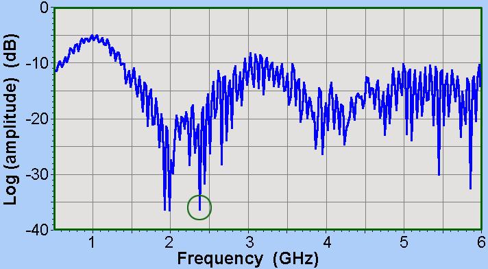
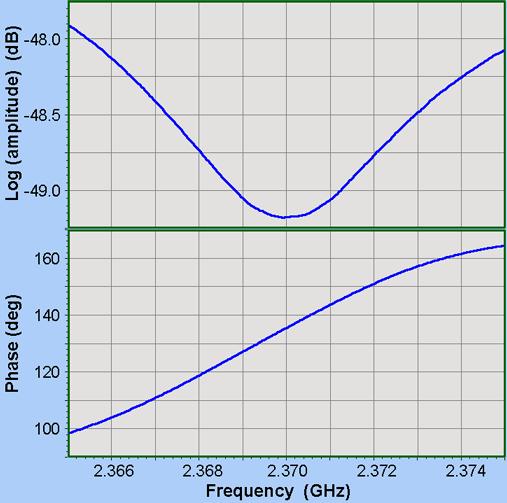
11 Experiments frequency sweep Page 11

12 DRAM Page 12


13 SMM image of SRAM A topography B capacitance C dc/dv Schematic of 6-FET unit cell of SRAM Page 13


14 KFM of SDRAM µm µm µm 0 V µm 0 60 µm 0 Topography Surface Potential Page 14


15 Images of an SDRAM Very high sensitivity Can see semiconductor, insulators and conductors Can be calibrated Can also get inductance and reactance Page 15


16 SMM image of SRAM Topography dc/dv Zoomed scans of a transistor. Line feature of nm in width can be seen in the dc/dv image Page 16
17 Carriers at 0V bias in SRAM Page 17

18 SiGe device Topography Capacitance dc/dv Page 18
 to the subcollector layer (1) with different doping levels were clearly resolved in the impedance image. (Sample courtesy of T.")
19 InGaP/GaAs heterojunction bipolar transistor Topography Impedance Different regions from the emitter-side contact layer (7 and 8) to the subcollector layer (1) with different doping levels were clearly resolved in the impedance image. (Sample courtesy of T. Low) Page 19

20 Biological sample Bacteria cells of geobacter sulfurreducens Topography Impedance Sample courtesy of N. Hansmeier, T. Chau, R. Ros, and S. Lindsay at Arizona State University. Page 20
21 Summary A new technique, which integrates AFM with a professional network analyzer, has been developed. scanning microwave microscopy Mapping impedance, capacitance, dielectric constants, etc. SNMM Measuring two-dimensional dopant density of semiconductors. SCM High sensitivity with resolution ultimately limited by the probe. Metals, semiconductors, dielectric materials, ferroelectric materials, insulators, and even biological samples. Page 21


 The MW")
22 Agilent Technologies = Innovation in Measurements We are presenting a state of the art AFM/SMM microscope to enable material measurements at the Nanoscale + = Coaxial cable Coaxial Resonator Sample Sample scanning AFM in X and Y and Z (closed loop) The MW diplexer Ground/Shield Network Analyzer Page 22
Electrical Characterization with SPM Application Modules
 Electrical Characterization with SPM Application Modules Metrology, Characterization, Failure Analysis: Data Storage Magnetoresistive (MR) read-write heads Semiconductor Transistors Interconnect Ferroelectric
Other SPM Techniques. Scanning Probe Microscopy HT10
 Other SPM Techniques Scanning Near-Field Optical Microscopy (SNOM) Scanning Capacitance Microscopy (SCM) Scanning Spreading Resistance Microscopy (SSRM) Multiprobe techniques Electrostatic Force Microscopy,
Intermittent-Contact Mode Force Microscopy & Electrostatic Force Microscopy (EFM)
") WORKSHOP Nanoscience on the Tip Intermittent-Contact Mode Force Microscopy & Electrostatic Force Microscopy (EFM) Table of Contents: 1. Motivation... 1. Simple Harmonic Motion... 1 3. AC-Mode Imaging...
WORKSHOP Nanoscience on the Tip Intermittent-Contact Mode Force Microscopy & Electrostatic Force Microscopy (EFM) Table of Contents: 1. Motivation... 1. Simple Harmonic Motion... 1 3. AC-Mode Imaging...
Magnetic Force Microscopy (MFM) F = µ o (m )H
 F = µ o (m )H") Magnetic Force Microscopy (MFM) F = µ o (m )H 1. MFM is based on the use of a ferromagnetic tip as a local field sensor. Magnetic interaction between the tip and the surface results in a force acting on
Magnetic Force Microscopy (MFM) F = µ o (m )H 1. MFM is based on the use of a ferromagnetic tip as a local field sensor. Magnetic interaction between the tip and the surface results in a force acting on
AFM Imaging In Liquids. W. Travis Johnson PhD Agilent Technologies Nanomeasurements Division
 AFM Imaging In Liquids W. Travis Johnson PhD Agilent Technologies Nanomeasurements Division Imaging Techniques: Scales Proteins 10 nm Bacteria 1μm Red Blood Cell 5μm Human Hair 75μm Si Atom Spacing 0.4nm
Scanning Probe Microscopy (SPM)
") http://ww2.sljus.lu.se/staff/rainer/spm.htm Scanning Probe Microscopy (FYST42 / FAFN30) Scanning Probe Microscopy (SPM) overview & general principles March 23 th, 2018 Jan Knudsen, room K522, jan.knudsen@sljus.lu.se
http://ww2.sljus.lu.se/staff/rainer/spm.htm Scanning Probe Microscopy (FYST42 / FAFN30) Scanning Probe Microscopy (SPM) overview & general principles March 23 th, 2018 Jan Knudsen, room K522, jan.knudsen@sljus.lu.se
Microwave imaging at the nanoscale: quantitative measurements for semiconductor devices, materials science and bio-applications
 Microwave imaging at the nanoscale: quantitative measurements for semiconductor devices, materials science and bio-applications Ferry Kienberger, Keysight Labs Austria This article will examine a novel
Scanning Tunneling Microscopy
 Scanning Tunneling Microscopy Scanning Direction References: Classical Tunneling Quantum Mechanics Tunneling current Tunneling current I t I t (V/d)exp(-Aφ 1/2 d) A = 1.025 (ev) -1/2 Å -1 I t = 10 pa~10na
Imaging Nucleic Acids with the AFM. W Travis Johnson PhD Agilent Technologies Nanomeasurements Division
 Imaging Nucleic Acids with the AFM W Travis Johnson PhD Agilent Technologies Nanomeasurements Division Structure of DNA A T G C Standard Watson-Crick A-T & G-C base pairs in B-DNA DNA double helix composed
Non-Sinusoidal Waves on (Mostly Lossless)Transmission Lines
Transmission Lines") Non-Sinusoidal Waves on (Mostly Lossless)Transmission Lines Don Estreich Salazar 21C Adjunct Professor Engineering Science October 212 https://www.iol.unh.edu/services/testing/sas/tools.php 1 Outline of
Non-Sinusoidal Waves on (Mostly Lossless)Transmission Lines Don Estreich Salazar 21C Adjunct Professor Engineering Science October 212 https://www.iol.unh.edu/services/testing/sas/tools.php 1 Outline of
NIS: what can it be used for?
 AFM @ NIS: what can it be used for? Chiara Manfredotti 011 670 8382/8388/7879 chiara.manfredotti@to.infn.it Skype: khiaram 1 AFM: block scheme In an Atomic Force Microscope (AFM) a micrometric tip attached
CNPEM Laboratório de Ciência de Superfícies
 Investigating electrical charged samples by scanning probe microscopy: the influence to magnetic force microscopy and atomic force microscopy phase images. Carlos A. R. Costa, 1 Evandro M. Lanzoni, 1 Maria
Scanning Probe Microscopy (SPM)
") Scanning Probe Microscopy (SPM) Scanning Tunneling Microscopy (STM) --- G. Binnig, H. Rohrer et al, (1982) Near-Field Scanning Optical Microscopy (NSOM) --- D. W. Pohl (1982) Atomic Force Microscopy (AFM)
Scanning Probe Microscopy (SPM) Scanning Tunneling Microscopy (STM) --- G. Binnig, H. Rohrer et al, (1982) Near-Field Scanning Optical Microscopy (NSOM) --- D. W. Pohl (1982) Atomic Force Microscopy (AFM)
Supplementary Information for. Effect of Ag nanoparticle concentration on the electrical and
 Supplementary Information for Effect of Ag nanoparticle concentration on the electrical and ferroelectric properties of Ag/P(VDF-TrFE) composite films Haemin Paik 1,2, Yoon-Young Choi 3, Seungbum Hong
The most versatile AFM platform for your nanoscale microscopy needs
 The most versatile AFM platform for your nanoscale microscopy needs Atomic Force Microscopy (AFM) for nanometer resolution imaging with electrical, magnetic, thermal, and mechanical property measurement
Nitride HFETs applications: Conductance DLTS
 Nitride HFETs applications: Conductance DLTS The capacitance DLTS cannot be used for device trap profiling as the capacitance for the gate will be very small Conductance DLTS is similar to capacitance
Nanometer-Scale Materials Contrast Imaging with a Near-Field Microwave Microscope
 Nanometer-Scale Materials Contrast Imaging with a Near-Field Microwave Microscope Atif Imtiaz 1 and Steven M. Anlage Center for Superconductivity Research, Department of Physics, University of Maryland,
Dopant Concentration Measurements by Scanning Force Microscopy
 73.40L Scanning Microsc. Microanal. Microstruct. 551 Classification Physics Abstracts - - 61.16P 73.00 Dopant Concentration Measurements by Scanning Force Microscopy via p-n Junctions Stray Fields Jacopo
Imaging Methods: Scanning Force Microscopy (SFM / AFM)
") Imaging Methods: Scanning Force Microscopy (SFM / AFM) The atomic force microscope (AFM) probes the surface of a sample with a sharp tip, a couple of microns long and often less than 100 Å in diameter.
Imaging Methods: Scanning Force Microscopy (SFM / AFM) The atomic force microscope (AFM) probes the surface of a sample with a sharp tip, a couple of microns long and often less than 100 Å in diameter.
Atomic Force Microscopy imaging and beyond
 Atomic Force Microscopy imaging and beyond Arif Mumtaz Magnetism and Magnetic Materials Group Department of Physics, QAU Coworkers: Prof. Dr. S.K.Hasanain M. Tariq Khan Alam Imaging and beyond Scanning
Electrostatic Force Microscopy (EFM)
") 6 Electrostatic Force Microscopy (EFM) Masakazu Nakamura and Hirofumi Yamada 1 Department of Electronics and Mechanical Engineering, Faculty of Engineering, Chiba University, 1-33 Yayoi-cho, Inage-ku,
6 Electrostatic Force Microscopy (EFM) Masakazu Nakamura and Hirofumi Yamada 1 Department of Electronics and Mechanical Engineering, Faculty of Engineering, Chiba University, 1-33 Yayoi-cho, Inage-ku,
Module 26: Atomic Force Microscopy. Lecture 40: Atomic Force Microscopy 3: Additional Modes of AFM
 Module 26: Atomic Force Microscopy Lecture 40: Atomic Force Microscopy 3: Additional Modes of AFM 1 The AFM apart from generating the information about the topography of the sample features can be used
Industrial standardization and quantification of the carrier concentration in semiconductor devices using electric SPM
 Paper Industrial standardization and quantification of the carrier concentration in semiconductor devices Takaya Fujita, 1 * Akiya Karen, 1,2 Hiroshi Ito 3 and Daisuke Fujita 4 1 Surface Analysis Laboratories,
Quantitative Scanning Capacitance Spectroscopy on GaAs and InAs Quantum Dots
 Quantitative Scanning Capacitance Spectroscopy on GaAs and InAs Quantum Dots W. Brezna, T. Roch, G. Strasser, J. Smoliner Institute of Solid State Electronics Vienna University of Technology, A-1040 Vienna,
Contents. Transmission Lines The Smith Chart Vector Network Analyser (VNA) ü structure ü calibration ü operation. Measurements
 ü structure ü calibration ü operation. Measurements") Contents Transmission Lines The Smith Chart Vector Network Analyser (VNA) ü structure ü calibration ü operation Measurements Göran Jönsson, EIT 2015-04-27 Vector Network Analysis 2 Waves on Lines If the
Contents Transmission Lines The Smith Chart Vector Network Analyser (VNA) ü structure ü calibration ü operation Measurements Göran Jönsson, EIT 2015-04-27 Vector Network Analysis 2 Waves on Lines If the
Instrumentation and Operation
 Instrumentation and Operation 1 STM Instrumentation COMPONENTS sharp metal tip scanning system and control electronics feedback electronics (keeps tunneling current constant) image processing system data
GHZ ELECTRICAL PROPERTIES OF CARBON NANOTUBES ON SILICON DIOXIDE MICRO BRIDGES
 GHZ ELECTRICAL PROPERTIES OF CARBON NANOTUBES ON SILICON DIOXIDE MICRO BRIDGES SHENG F. YEN 1, HAROON LAIS 1, ZHEN YU 1, SHENGDONG LI 1, WILLIAM C. TANG 1,2, AND PETER J. BURKE 1,2 1 Electrical Engineering
Basic Laboratory. Materials Science and Engineering. Atomic Force Microscopy (AFM)
") Basic Laboratory Materials Science and Engineering Atomic Force Microscopy (AFM) M108 Stand: 20.10.2015 Aim: Presentation of an application of the AFM for studying surface morphology. Inhalt 1.Introduction...
Basic Laboratory Materials Science and Engineering Atomic Force Microscopy (AFM) M108 Stand: 20.10.2015 Aim: Presentation of an application of the AFM for studying surface morphology. Inhalt 1.Introduction...
The needs and challenges of electrical measurements for micro/nanoelectronic devices.
 1 The needs and challenges of electrical measurements for micro/nanoelectronic devices. Brice Gautier N. Baboux, D. Albertini, S. Martin, W. Hourani, A. Grandfond Institut des Nanotechnologies de Lyon
Contents. Transmission Lines The Smith Chart Vector Network Analyser (VNA) ü structure ü calibration ü operation. Measurements
 ü structure ü calibration ü operation. Measurements") Contents Transmission Lines The Smith Chart Vector Network Analyser (VNA) ü structure ü calibration ü operation Measurements Göran Jönsson, EIT 2017-05-12 Vector Network Analysis 2 Waves on Lines If the
Contents Transmission Lines The Smith Chart Vector Network Analyser (VNA) ü structure ü calibration ü operation Measurements Göran Jönsson, EIT 2017-05-12 Vector Network Analysis 2 Waves on Lines If the
SMM EMPro. Introduction
 SMM EMPro Introduction In this application note, we describe electromagnetic (EM) simulations using the Keysight Technologies, Inc. EMPro software 1 to support the interpretation of scanning microwave
Atomic and molecular interactions. Scanning probe microscopy.
 Atomic and molecular interactions. Scanning probe microscopy. Balázs Kiss Nanobiotechnology and Single Molecule Research Group, Department of Biophysics and Radiation Biology 27. November 2013. 2 Atomic
Characterization of MEMS Devices
 MEMS: Characterization Characterization of MEMS Devices Prasanna S. Gandhi Assistant Professor, Department of Mechanical Engineering, Indian Institute of Technology, Bombay, Recap Characterization of MEMS
Expanding Characterization of Materials with Kelvin Force Microscopy
 Expanding Characterization of Materials with Kelvin Force Microscopy Sergei Magonov Page 1 Outline Introduction to Kelvin Force Microscopy Different KFM Modes and Their Practical Evaluation Applications
Lecture 4 Scanning Probe Microscopy (SPM)
") Lecture 4 Scanning Probe Microscopy (SPM) General components of SPM; Tip --- the probe; Cantilever --- the indicator of the tip; Tip-sample interaction --- the feedback system; Scanner --- piezoelectric
Lecture 4 Scanning Probe Microscopy (SPM) General components of SPM; Tip --- the probe; Cantilever --- the indicator of the tip; Tip-sample interaction --- the feedback system; Scanner --- piezoelectric
STM: Scanning Tunneling Microscope
 STM: Scanning Tunneling Microscope Basic idea STM working principle Schematic representation of the sample-tip tunnel barrier Assume tip and sample described by two infinite plate electrodes Φ t +Φ s =
Measurement of hardness, surface potential, and charge distribution with dynamic contact mode electrostatic force microscope
 REVIEW OF SCIENTIFIC INSTRUMENTS VOLUME 70, NUMBER 3 MARCH 1999 Measurement of hardness, surface potential, and charge distribution with dynamic contact mode electrostatic force microscope J. W. Hong,
Contents. ! Transmission Lines! The Smith Chart! Vector Network Analyser (VNA) ! Measurements. ! structure! calibration! operation
 ! Measurements. ! structure! calibration! operation") Contents! Transmission Lines! The Smith Chart! Vector Network Analyser (VNA)! structure! calibration! operation! Measurements Göran Jönsson, EIT 2009-11-16 Network Analysis 2! Waves on Lines! If the wavelength
Contents! Transmission Lines! The Smith Chart! Vector Network Analyser (VNA)! structure! calibration! operation! Measurements Göran Jönsson, EIT 2009-11-16 Network Analysis 2! Waves on Lines! If the wavelength
Institute for Electron Microscopy and Nanoanalysis Graz Centre for Electron Microscopy
 Institute for Electron Microscopy and Nanoanalysis Graz Centre for Electron Microscopy Micromechanics Ass.Prof. Priv.-Doz. DI Dr. Harald Plank a,b a Institute of Electron Microscopy and Nanoanalysis, Graz
High-resolution Magnetic Force Microscope
 High-resolution Magnetic Force Microscope hr-mfm Gigasteps on a nanoscale hr-mfm the key instrument for research and development of high-density magnetic media. 1 nm magnetic resolution guaranteed. Winner
SUPPLEMENTARY INFORMATION
 SUPPLEMENTARY INFORMATION Insulating Interlocked Ferroelectric and Structural Antiphase Domain Walls in Multiferroic YMnO 3 T. Choi 1, Y. Horibe 1, H. T. Yi 1,2, Y. J. Choi 1, Weida. Wu 1, and S.-W. Cheong
Calibrated complex impedance of CHO cells and E. coli bacteria at GHz frequencies using scanning microwave microscopy
 Nanotechnology PAPER OPEN ACCESS Calibrated complex impedance of CHO cells and E. coli bacteria at GHz frequencies using scanning microwave microscopy To cite this article: Silviu-Sorin Tuca et al 2016
MSE 310/ECE 340: Electrical Properties of Materials Fall 2014 Department of Materials Science and Engineering Boise State University
 MSE 310/ECE 340: Electrical Properties of Materials Fall 2014 Department of Materials Science and Engineering Boise State University Practice Final Exam 1 Read the questions carefully Label all figures
Application of electrostatic force microscopy in nanosystem diagnostics
 Materials Science, Vol., No. 3, 003 Application of electrostatic force microscopy in nanosystem diagnostics TEODOR P. GOTSZALK *, PIOTR GRABIEC, IVO W. RANGELOW 3 Fulty of Microsystem Electronics and Photonics,
Nanoscale. Probing resistivity and doping concentration of semiconductors at the nanoscale using scanning microwave microscopy PAPER. 1.
 PAPER ite this:, 2015, 7, 14715 Probing resistivity and doping concentration of semiconductors at the nanoscale using scanning microwave microscopy Enrico Brinciotti, a Georg Gramse, b Soeren Hommel, c
AFM for Measuring Surface Topography and Forces
 ENB 2007 07.03.2007 AFM for Measuring Surface Topography and Forces Andreas Fery Scanning Probe : What is it and why do we need it? AFM as a versatile tool for local analysis and manipulation Dates Course
Scanning capacitance spectroscopy of an Al x Ga 1Àx NÕGaN heterostructure field-effect transistor structure: Analysis of probe tip effects
 Scanning capacitance spectroscopy of an Al x Ga 1Àx NÕGaN heterostructure field-effect transistor structure: Analysis of probe tip effects D. M. Schaadt and E. T. Yu a) Department of Electrical and Computer
Scanning gate microscopy and individual control of edge-state transmission through a quantum point contact
 Scanning gate microscopy and individual control of edge-state transmission through a quantum point contact Stefan Heun NEST, CNR-INFM and Scuola Normale Superiore, Pisa, Italy Coworkers NEST, Pisa, Italy:
Introduction to Scanning Probe Microscopy Zhe Fei
 Introduction to Scanning Probe Microscopy Zhe Fei Phys 590B, Apr. 2019 1 Outline Part 1 SPM Overview Part 2 Scanning tunneling microscopy Part 3 Atomic force microscopy Part 4 Electric & Magnetic force
Supplementary Methods A. Sample fabrication
 Supplementary Methods A. Sample fabrication Supplementary Figure 1(a) shows the SEM photograph of a typical sample, with three suspended graphene resonators in an array. The cross-section schematic is
From nanophysics research labs to cell phones. Dr. András Halbritter Department of Physics associate professor
 From nanophysics research labs to cell phones Dr. András Halbritter Department of Physics associate professor Curriculum Vitae Birth: 1976. High-school graduation: 1994. Master degree: 1999. PhD: 2003.
Nanometrology and its role in the development of nanotechnology
 Nanometrology and its role in the development of nanotechnology Rob Bergmans Nederlands Meetinstituut Van Swinden Laboratorium 1 NMi Van Swinden Laboratorium The Art of Measurement Dutch national metrology
High-resolution Characterization of Organic Ultrathin Films Using Atomic Force Microscopy
 High-resolution Characterization of Organic Ultrathin Films Using Atomic Force Microscopy Jing-jiang Yu Nanotechnology Measurements Division Agilent Technologies, Inc. Atomic Force Microscopy High-Resolution
Please allow us to demonstrate our capabilities and test us testing your samples!
 We determine properties of surfaces, thin films, and layer structures Hardness Young s modulus Scratch, friction, and wear tests Topography Mapping of thermal, magnetic, and electronic properties Please
nano-ta: Nano Thermal Analysis
 nano-ta: Nano Thermal Analysis Application Note #1 Failure Analysis - Identification of Particles in a Polymer Film Author: David Grandy Ph.D. Introduction Nano-TA is a local thermal analysis technique
Waves on Lines. Contents. ! Transmission Lines! The Smith Chart! Vector Network Analyser (VNA) ! Measurements
 ! Measurements") Waves on Lines If the wavelength to be considered is significantly greater compared to the size of the circuit the voltage will be independent of the location. amplitude d! distance but this is not true
Waves on Lines If the wavelength to be considered is significantly greater compared to the size of the circuit the voltage will be independent of the location. amplitude d! distance but this is not true
Outline of College Physics OpenStax Book
 Outline of College Physics OpenStax Book Taken from the online version of the book Dec. 27, 2017 18. Electric Charge and Electric Field 18.1. Static Electricity and Charge: Conservation of Charge Define
Time Domain Reflectometry Theory
 Time Domain Reflectometry Theory Application Note 304-2 For Use with Agilent 8600B Infiniium DCA Introduction The most general approach to evaluating the time domain response of any electromagnetic system
Scanning Probe Microscopy. Amanda MacMillan, Emmy Gebremichael, & John Shamblin Chem 243: Instrumental Analysis Dr. Robert Corn March 10, 2010
 Scanning Probe Microscopy Amanda MacMillan, Emmy Gebremichael, & John Shamblin Chem 243: Instrumental Analysis Dr. Robert Corn March 10, 2010 Scanning Probe Microscopy High-Resolution Surface Analysis
Magnetic Resonance Force Microscopy. Christian Degen Department of Physics, ETH Zurich, Switzerland
 Magnetic Resonance Force Microscopy Christian Degen Department of Physics, ETH Zurich, Switzerland CIMST Summer School 2014 From Andreas Trabesinger / Wikipedia Scale of things 1m 1mm 1µm 1-100 nm 1nm
PY5020 Nanoscience Scanning probe microscopy
 PY500 Nanoscience Scanning probe microscopy Outline Scanning tunnelling microscopy (STM) - Quantum tunnelling - STM tool - Main modes of STM Contact probes V bias Use the point probes to measure the local
Metrology is not a cost factor, but a profit center
 Edition February 2018 Semiconductor technology & processing Metrology is not a cost factor, but a profit center In recent years, remarkable progress has been made in the field of metrology, which is crucial
MEMS Metrology. Prof. Tianhong Cui ME 8254
 MEMS Metrology Prof. Tianhong Cui ME 8254 What is metrology? Metrology It is the science of weights and measures Refers primarily to the measurements of length, weight, time, etc. Mensuration- A branch
Scanning probe studies of the electrical activity at interfaces formed by silicon wafer direct bonding
 phys. stat. sol. (c) 4, No. 8, 893 897 (007) / DOI 10.100/pssc.00675481 Scanning probe studies of the electrical activity at interfaces formed by silicon wafer direct bonding M. Ratzke *, 1,, O. Vyvenko
Lecture 6 PN Junction and MOS Electrostatics(III) Metal-Oxide-Semiconductor Structure
 Metal-Oxide-Semiconductor Structure") Lecture 6 PN Junction and MOS Electrostatics(III) Metal-Oxide-Semiconductor Structure Outline 1. Introduction to MOS structure 2. Electrostatics of MOS in thermal equilibrium 3. Electrostatics of MOS with
Lecture 6 PN Junction and MOS Electrostatics(III) Metal-Oxide-Semiconductor Structure Outline 1. Introduction to MOS structure 2. Electrostatics of MOS in thermal equilibrium 3. Electrostatics of MOS with
Single- and Multiport Networks. RF Electronics Spring, 2018 Robert R. Krchnavek Rowan University
 Single- and Multiport Networks RF Electronics Spring, 208 Robert R. Krchnavek Rowan University Objectives Generate an understanding of the common network representations of Z, Y, h, and ABCD. To be able
Consulting Service measurements Project collaboration Training & Education. Swiss Scanning Probe Microscopy User Laboratory
 Consulting Service measurements Project collaboration Training & Education Swiss Scanning Probe Microscopy User Laboratory Prof. Dr Hans Josef Hug Welcome to SUL, the Swiss Scanning Probe Microscopy User
Microwave Loss Reduction in Cryogenically Cooled Conductors R. Finger and A. R. Kerr
 NATIONAL RADIO ASTRONOMY OBSERVATORY ELECTRONICS DIVISION INTERNAL REPORT NO. 321 Microwave Loss Reduction in Cryogenically Cooled Conductors R. Finger and A. R. Kerr July 3, 2008 NATIONAL RADIO ASTRONOMY
ECE 2112 ELECTROMAGNETIC THEORY C-term 2018
 Worcester Polytechnic Institute Department of Electrical and Computer Engineering ECE 2112 ELECTROMAGNETIC THEORY C-term 2018 Professor: Dr. Reinhold Ludwig Office: AK 229, Tel.: 508-831-5315 Office hours:
Scanning Probe Microscopy (SPM)
") CHEM53200: Lecture 9 Scanning Probe Microscopy (SPM) Major reference: 1. Scanning Probe Microscopy and Spectroscopy Edited by D. Bonnell (2001). 2. A practical guide to scanning probe microscopy by Park
CHEM53200: Lecture 9 Scanning Probe Microscopy (SPM) Major reference: 1. Scanning Probe Microscopy and Spectroscopy Edited by D. Bonnell (2001). 2. A practical guide to scanning probe microscopy by Park
arxiv: v1 [physics.acc-ph] 19 Jan 2012
![arxiv: v1 [physics.acc-ph] 19 Jan 2012](/thumbs/71/65761722.jpg "arxiv: v1 [physics.acc-ph] 19 Jan 2012") RF engineering basic concepts: the Smith chart F. Caspers CERN, Geneva, Switzerland arxiv:68v [physics.acc-ph] 9 Jan Motivation Abstract The Smith chart is a very valuable and important tool that facilitates
RF engineering basic concepts: the Smith chart F. Caspers CERN, Geneva, Switzerland arxiv:68v [physics.acc-ph] 9 Jan Motivation Abstract The Smith chart is a very valuable and important tool that facilitates
Atomic Force Microscopy (AFM) Part I
 Part I") Atomic Force Microscopy (AFM) Part I CHEM-L2000 Eero Kontturi 6 th March 2018 Lectures on AFM Part I Principles and practice Imaging of native materials, including nanocellulose Part II Surface force measurements
Atomic Force Microscopy (AFM) Part I CHEM-L2000 Eero Kontturi 6 th March 2018 Lectures on AFM Part I Principles and practice Imaging of native materials, including nanocellulose Part II Surface force measurements
Nanotechnology. Gavin Lawes Department of Physics and Astronomy
 Nanotechnology Gavin Lawes Department of Physics and Astronomy Earth-Moon distance 4x10 8 m (courtesy NASA) Length scales (Part I) Person 2m Magnetic nanoparticle 5x10⁻⁹ m 10 10 m 10 5 m 1 m 10-5 m 10-10
Calibration of Shielded Microwave Probes Using Bulk Dielectrics
 Calibration of Shielded Microwave Probes Using Bulk Dielectrics K. Lai, W. Kundhikanjana, M.A. Kelly, Z.X. Shen Department of Applied Physics and Geballe Laboratory for Advanced Materials Stanford University,
PHYSICS Course Structure Units Topics Marks Electrostatics Current Electricity III Magnetic Effect of Current & Magnetism
 PHYSICS Course Structure Units Topics Marks I Chapter 1 Chapter 2 II Chapter 3 III Chapter 4 Chapter 5 IV Chapter 6 Chapter 7 V Chapter 8 VI Chapter 9 Electrostatics Electric Charges and Fields Electrostatic
And Manipulation by Scanning Probe Microscope
 Basic 15 Nanometer Scale Measurement And Manipulation by Scanning Probe Microscope Prof. K. Fukuzawa Dept. of Micro/Nano Systems Engineering Nagoya University I. Basics of scanning probe microscope Basic
Keysight Technologies Advanced Atomic Force Microscopy: Exploring Measurements of Local Electric Properties. Application Note
 Keysight Technologies Advanced Atomic Force Microscopy: Exploring Measurements of Local Electric Properties Application Note Introduction In the past two decades Atomic Force Microscopy (AFM) 1 has been
ELECTROMAGNETISM. Second Edition. I. S. Grant W. R. Phillips. John Wiley & Sons. Department of Physics University of Manchester
 ELECTROMAGNETISM Second Edition I. S. Grant W. R. Phillips Department of Physics University of Manchester John Wiley & Sons CHICHESTER NEW YORK BRISBANE TORONTO SINGAPORE Flow diagram inside front cover
Electronic Quantum Transport in Mesoscopic Semiconductor Structures
 Thomas Ihn Electronic Quantum Transport in Mesoscopic Semiconductor Structures With 90 Illustrations, S in Full Color Springer Contents Part I Introduction to Electron Transport l Electrical conductance
SCANNING-PROBE TECHNIQUES OR APPARATUS; APPLICATIONS OF SCANNING-PROBE TECHNIQUES, e.g. SCANNING PROBE MICROSCOPY [SPM]
![SCANNING-PROBE TECHNIQUES OR APPARATUS; APPLICATIONS OF SCANNING-PROBE TECHNIQUES, e.g. SCANNING PROBE MICROSCOPY [SPM]](/thumbs/81/83165631.jpg "SCANNING-PROBE TECHNIQUES OR APPARATUS; APPLICATIONS OF SCANNING-PROBE TECHNIQUES, e.g. SCANNING PROBE MICROSCOPY [SPM]") G01Q SCANNING-PROBE TECHNIQUES OR APPARATUS; APPLICATIONS OF SCANNING-PROBE TECHNIQUES, e.g. SCANNING PROBE MICROSCOPY [SPM] Scanning probes, i.e. devices having at least a tip of nanometre sized dimensions
G01Q SCANNING-PROBE TECHNIQUES OR APPARATUS; APPLICATIONS OF SCANNING-PROBE TECHNIQUES, e.g. SCANNING PROBE MICROSCOPY [SPM] Scanning probes, i.e. devices having at least a tip of nanometre sized dimensions
Supporting Information. Real-time nanoscale open-circuit voltage dynamics of perovskite solar cells
 Supporting Information Real-time nanoscale open-circuit voltage dynamics of perovskite solar cells Joseph L. Garrett 1,2, Elizabeth M. Tennyson 2,3,Miao Hu 4, Jinsong Huang 4, Jeremy N. Munday 2,5*, Marina
Session 6: Solid State Physics. Diode
 Session 6: Solid State Physics Diode 1 Outline A B C D E F G H I J 2 Definitions / Assumptions Homojunction: the junction is between two regions of the same material Heterojunction: the junction is between
MS482 Materials Characterization ( 재료분석 ) Lecture Note 11: Scanning Probe Microscopy. Byungha Shin Dept. of MSE, KAIST
 Lecture Note 11: Scanning Probe Microscopy. Byungha Shin Dept. of MSE, KAIST") 2015 Fall Semester MS482 Materials Characterization ( 재료분석 ) Lecture Note 11: Scanning Probe Microscopy Byungha Shin Dept. of MSE, KAIST 1 Course Information Syllabus 1. Overview of various characterization
2015 Fall Semester MS482 Materials Characterization ( 재료분석 ) Lecture Note 11: Scanning Probe Microscopy Byungha Shin Dept. of MSE, KAIST 1 Course Information Syllabus 1. Overview of various characterization
AISSCE 2016 EXPECTED (SURE SHORT) QUESTIONS WEIGHTAGE-WISE 2016
 QUESTIONS WEIGHTAGE-WISE 2016") CLASS: XII AISSCE 2016 Subject: Physics EXPECTED (SURE SHORT) QUESTIONS WEIGHTAGE-WISE 2016 Q3 Section A ( 1 Mark ) A force F is acting between two charges placed some distances apart in vacuum. If a brass
CLASS: XII AISSCE 2016 Subject: Physics EXPECTED (SURE SHORT) QUESTIONS WEIGHTAGE-WISE 2016 Q3 Section A ( 1 Mark ) A force F is acting between two charges placed some distances apart in vacuum. If a brass
Supplementary Figure 1 a) Scheme of microfluidic device fabrication by photo and soft lithography,
 Scheme of microfluidic device fabrication by photo and soft lithography,") a b 1 mm Supplementary Figure 1 a) Scheme of microfluidic device fabrication by photo and soft lithography, (a1, a2) 50nm Pd evaporated on Si wafer with 100 nm Si 2 insulating layer and 5nm Cr as an adhesion
a b 1 mm Supplementary Figure 1 a) Scheme of microfluidic device fabrication by photo and soft lithography, (a1, a2) 50nm Pd evaporated on Si wafer with 100 nm Si 2 insulating layer and 5nm Cr as an adhesion
Electrochemically Exfoliated Graphene as Solution-Processable, Highly-Conductive Electrodes for Organic Electronics
 Supporting Information Electrochemically Exfoliated Graphene as Solution-Processable, Highly-Conductive Electrodes for Organic Electronics Khaled Parvez, Rongjin Li, Sreenivasa Reddy Puniredd, Yenny Hernandez,
Erik Lind
 High-Speed Devices, 2011 Erik Lind (Erik.Lind@ftf.lth.se) Course consists of: 30 h Lectures (H322, and Fys B check schedule) 8h Excercises 2x2h+4h Lab Excercises (2 Computer simulations, 4 RF measurment
EMPIR 14IND07 3DStack. Guide for conformity assessment for electrical and thermal properties of TSVs
 EMPIR 14IND07 3DStack Guide for conformity assessment for electrical and thermal properties of TSVs Michele Stucchi and Ingrid De Wolf, IMEC Nicolas Devanciard, Carlos Beitia, CEA José Morán, Alexandra
Contents. What is AFM? History Basic principles and devices Operating modes Application areas Advantages and disadvantages
 Contents What is AFM? History Basic principles and devices Operating modes Application areas Advantages and disadvantages Figure1: 2004 Seth Copen Goldstein What is AFM? A type of Scanning Probe Microscopy
MSN551 LITHOGRAPHY II
 MSN551 Introduction to Micro and Nano Fabrication LITHOGRAPHY II E-Beam, Focused Ion Beam and Soft Lithography Why need electron beam lithography? Smaller features are required By electronics industry:
Nanomechanics Measurements and Standards at NIST
 Nanomechanics Measurements and Standards at NIST Robert F. Cook Deputy Chief, Ceramics Division Leader, Nanomechanical Properties Group robert.cook@nist.gov NIST Mission Promote U.S. innovation and industrial
Optics and Spectroscopy
 Introduction to Optics and Spectroscopy beyond the diffraction limit Chi Chen 陳祺 Research Center for Applied Science, Academia Sinica 2015Apr09 1 Light and Optics 2 Light as Wave Application 3 Electromagnetic
Supplemental material: Transient thermal characterization of suspended monolayer MoS 2
 Supplemental material: Transient thermal characterization of suspended monolayer MoS Robin J. Dolleman,, David Lloyd, Martin Lee, J. Scott Bunch,, Herre S. J. van der Zant, and Peter G. Steeneken, Kavli
Asylum Research. AFM Tools for Nanoscale Electrical Characterization. Abstract. Introduction. Conductive AFM
 AFM Asylum Research AFM Tools for Nanoscale Electrical Characterization Abstract The importance of characterizing electrical functionality on nanometer length scales continues to grow as devices shrink
A tomic Force Microscopy (AFM) has been extensively used to measure electrical properties of a sample at
 has been extensively used to measure electrical properties of a sample at") OPEN SUBJECT AREAS: ATOMIC FORCE MICROSCOPY IMAGING TECHNIQUES Received 23 September 2013 Accepted 8 November 2013 Published 27 November 2013 Correspondence and requests for materials should be addressed
OPEN SUBJECT AREAS: ATOMIC FORCE MICROSCOPY IMAGING TECHNIQUES Received 23 September 2013 Accepted 8 November 2013 Published 27 November 2013 Correspondence and requests for materials should be addressed
Practical aspects of Kelvin probe force microscopy
 REVIEW OF SCIENTIFIC INSTRUMENTS VOLUME 70, NUMBER 3 MARCH 1999 Practical aspects of Kelvin probe force microscopy H. O. Jacobs, H. F. Knapp, and A. Stemmer a) Swiss Federal Institute of Technology, Nanotechnology
Metal-oxide-semiconductor field effect transistors (2 lectures)
") Metal-ide-semiconductor field effect transistors ( lectures) MOS physics (brief in book) Current-voltage characteristics - pinch-off / channel length modulation - weak inversion - velocity saturation -
Metal-ide-semiconductor field effect transistors ( lectures) MOS physics (brief in book) Current-voltage characteristics - pinch-off / channel length modulation - weak inversion - velocity saturation -
Combined AFM and Raman Enables: Comprehensive Data Using Optical, AFM, and Spectroscopic Methods
 Combined AFM and Raman Enables: Comprehensive Data Using Optical, AFM, and Spectroscopic Methods Dark field: sees cracks, and contamination: - Pick appropriate area for AFM scan AFM: real 3D morphology
(Scanning Probe Microscopy)
") (Scanning Probe Microscopy) Ing-Shouh Hwang (ishwang@phys.sinica.edu.tw) Institute of Physics, Academia Sinica, Taipei, Taiwan References 1. G. Binnig, H. Rohrer, C. Gerber, and Weibel, Phys. Rev. Lett.
(Scanning Probe Microscopy) Ing-Shouh Hwang (ishwang@phys.sinica.edu.tw) Institute of Physics, Academia Sinica, Taipei, Taiwan References 1. G. Binnig, H. Rohrer, C. Gerber, and Weibel, Phys. Rev. Lett.
Ballistic transport at GHz frequencies in ungated HEMT structures
 Solid-State Electronics 8 (2) 23 27 www.elsevier.com/locate/sse Ballistic transport at GHz frequencies in ungated HEMT structures Sungmu Kang a, Peter J. Burke a, *, L.N. Pfeiffer b, K.W. West b a Henry