Nanoscale infrared spectroscopy
|
|
|
- Lee Payne
- 5 years ago
- Views:
Transcription


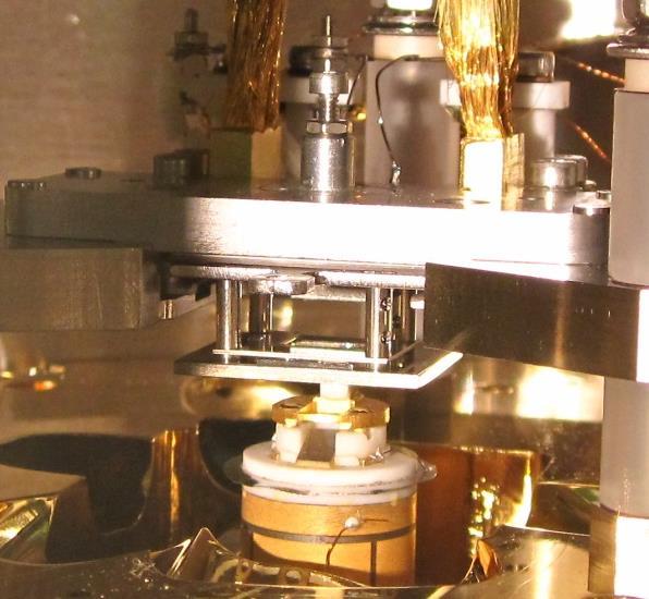
1 Nanoscale infrared spectroscopy In the early days of scanning probe microscopy, researchers and instrumentation developers were often postulating about the future and, perhaps one day, the advent of the lab-on-a-tip. While the technology has seen the development of highly spatially resolved topography imaging coupled to a series of different physical measurements, it is only recently that is has been possible to perform chemical characterization measurements with infrared spectroscopy on the nanoscale. The enabling technique is known as nanoir. Craig Prater*, Kevin Kjoller and Roshan Shetty, Anasys Instruments, Santa Barbara, USA * craig@anasysinstruments.com For many years, infrared spectroscopy has provided the ability to characterize and identify chemical species. However, it has always been restricted to resolution in the order of 5 10 microns and then only when applying attenuated total reflection spectroscopy, ATR. Now, when combined with the nanoscale spatial resolution of an AFM tip, it is possible to measure and map local chemical composition below the diffraction limit of light. The technology described here as nanoir will also perform nanoscale topographic, mechanical and thermal analyses. This exciting and unique technology is provided through a new platform called nanoir (Anasys Instruments, Santa Barbara, CA). The nanoir is a probe-based measurement tool that reveals the chemical composition of samples at the nanoscale (Fig. 1). This laboratory solution combines key elements of both infrared spectroscopy and atomic force microscopy (AFM) to enable the acquisition of infrared spectra at spatial resolutions of nanometers, well beyond the optical diffraction limit. Potential application areas span polymer Fig. 1 NanoIR system. 56 NOVEMBER 2010 VOLUME 13 NUMBER 11 ISSN: Elsevier Ltd 2010 Open access under CC BY-NC-ND license.


2 Nanoscale infrared spectroscopy APPLICATION science, materials science, and life science, including detailed studies of structure-property correlations. The science behind the system applies the patent-pending technology of infrared nanospectroscopy, a technique pioneered by award-winning researcher Dr. Alexandre Dazzi of the Laboratoire de Chimie Physique,CLIO, Université Paris-Sud, Orsay, France. This is a photothermal method which follows the absorption of the infrared and the subsequent generation of heat. Instrumentation The nanoir system uses a pulsed, tunable IR source to excite molecular absorption in a sample that has been mounted on a ZnSe prism (Fig. 2). Samples are prepared in one of two ways. For many samples, ultramicrotomy is used to cut sections with thicknesses between 100 nm and 1000 nm. These are then transferred to the prism surface. In other sample preparations, it may be possible to cast thin films from solvent directly on the prism surface. The IR beam illuminates the sample by total internal reflection similar to conventional ATR spectroscopy (Fig. 3). As the sample absorbs radiation, it heats up, leading to rapid thermal expansion that excites resonant oscillations of the cantilever which is detected using the standard AFM photodiode measurement system. These induced oscillations decay in a characteristic ringdown which can be analyzed via Fourier techniques to extract the amplitudes and frequencies of the oscillations. Then, measuring the amplitudes of the cantilever oscillation as a function of the source wavelength, local absorption spectra are created. Fig. 2 Samples are mounted on a zinc selenide prism. Fig. 3. Schematic shows the illumination of the sample by the IR laser. Fig. 4. Schematic to illustrate the process of analyzing the ringdown of a cantilever to generate a familiar IR spectrum. NOVEMBER 2010 VOLUME 13 NUMBER 11 57


3 APPLICATION Nanoscale infrared spectroscopy The oscillation frequencies of the ringdown are also related to the mechanical stiffness of the sample. With maximum flexibility, the IR source can also be tuned to a single wavelength to simultaneously map surface topography, mechanical properties, and IR absorption in selected absorption bands Fig. 4. The results are spectacular as established analytical techniques are linked together as never before possible. The potential application areas are found in the polymer, materials and life sciences offering notable potential in producing detailed studies of structure-property correlations. The ability to combine nanoscale spatial resolution with chemical spectroscopy provides users of nanoir technology with the tools to quickly survey regions of a sample via AFM and then rapidly acquire high-resolution chemical spectra at selected regions on the sample. Making additional mechanical and thermal properties measurements with nanoscale resolution adds significantly to the power of this technique. Applying mid-ir spectroscopy The nanoir system enables researchers to harness the full power of mid-ir spectroscopy. The system s IR source, designed using proprietary technology, is continuously tunable from 3600 to 1200 cm -1. This range covers a major portion of the mid-ir, including important CH, NH, and CO bands, as well as carbonyl and amide I/II bands. Polymer spectra acquired with the nanoir system have demonstrated good correlation with bulk FTIR spectra. The nanoir software also allows researchers to export nanoscale IR absorption spectra to standard analysis packages (e.g., Bio-Rad s KnowItAll ) to rapidly analyze samples and identify chemical components. The nanoir software also allows integrated thermal and mechanical property mapping in addition to its ability to provide high-resolution infrared spectra. Mechanical properties of a sample can be collected using a contact resonance method to map stiffness variations simultaneously with the topography while the nanoir platform can also perform nanoscale thermal analysis providing researchers to work beyond bulk thermal analysis measurement to obtain information not available with any other technique. Applications of nanoir Polymer blends and composites Typical data sets will show deflection, IR absorption and stiffness. The images of two different polymer blend samples were taken by tuning the IR source to a fixed wavenumber and then scanning the sample while measuring the amplitude of the nanoir signal for the IR absorption and the frequency of the fundamental contact resonance for the stiffness. The first example is a sample which is 100% ABS, acrylonitrile butadiene styrene where the AS intermixes and the butadiene phase separates, Fig. 5. The butadiene is soft and so can easily be seen in the stiffness image. It also has a stronger absorption at 3025 cm -1. It is interesting to correlate the light areas in the IR absorption with the dark areas in the stiffness. These should be the same material but there are differences which may correlate with differences in thickness or whether the material is at the surface or subsurface. Fig. 5 Comparison of the deflection, infrared and stiffness signals of a sample of ABS. Fig. 6 A blend of ABS (40%) and polycarbonate (60%) mapping deflection, infrared and stiffness signals. 58 NOVEMBER 2010 VOLUME 13 NUMBER 11

 were embedded in epoxy to form a composite. It was microtomed before study. (Fig. 7).")
4 Nanoscale infrared spectroscopy APPLICATION Fig. 7 A polystyrene sphere in an epoxy matrix demonstrating the spatial resolution of the nanoir system. Note that a characteristic polystyrene spectrum is observed in the center, and edges of the PS bead, but a very different epoxy spectrum is observed just 100 nm across the material boundary. The second example is a blend of 40% ABS and 60% polycarbonate, Fig. 6. At 1780 cm -1 wavenumber, the polycarbonate exhibits a strong signal while the soft butadiene domains are clearly seen in the stiffness map. The next example is a sample where polystyrene spheres (PS) were embedded in epoxy to form a composite. It was microtomed before study. (Fig. 7). There is an absorption band at 3025 cm -1 which corresponds to the aromatic bonds in the polystyrene. This is clearly Fig. 8 The spectral mapping of a degradable polymer blend. NOVEMBER 2010 VOLUME 13 NUMBER 11 59
 Spectroscopic map showing different regions of the polymer composite; (c) Mechanical map showing the correlation between the CH absorption spectrum and the contact resonance frequency; (d) Point")
5 APPLICATION Nanoscale infrared spectroscopy (a) (c) (b) (d) Fig. 9(a) AFM topographic image clearly showing regions of nylon and ethylene co-acrylic acid (EAA). (b) Spectroscopic map showing different regions of the polymer composite; (c) Mechanical map showing the correlation between the CH absorption spectrum and the contact resonance frequency; (d) Point nanothermomechanical analysis data showing the different softening points of the nylon and EAA regions. seen in the spectra taken from the center of the PS sphere and is also clearly resolved in spectra that were taken within ~100 nm of the interface and is not seen in the epoxy. This is a good resolution test for the nanoir technique. Degradable polymers In this example, the spectral mapping of a degradable polymer blend is shown. The AFM measurements allow spatial mapping of polymer matrix and additives. The nanoir can then spatially map the variations in chemical components. These are then interpreted In the line spectral map noting the spatially varying concentration of the C=O carbonyl band (1740 cm -1 ) and the single bond C-O peak at around 1100 cm -1. This data is summarized in Fig. 8. Multifunctional measurements on a composite With the nanoir system provides the capability of multifunctional measurements. These enable a more complete picture of samples, integrating topographic, spectroscopic, mechanical and thermal property data. High resolution topographic measurements are performed by AFM, Fig. 9a, while the nanoscale infrared spectroscopy technique enables both local chemical characterization and contact resonance frequency measurements to be made, Figs. 9b and 9c. Going one stage further, the system accommodates thermal probes to give thermomechanical measurements again with spatial resolution on the nanoscale, Fig. 9d. Looking forward applications developments The nanoir system combines infrared spectroscopy and atomic force microscopy to provide high resolution topographic, chemical, mechanical and thermal mapping. This combination provides spatial resolution at length scales well below the diffraction limit of conventional IR spectroscopy and adds chemical spectroscopy to the field of atomic force microscopy. The potential for future applications is very broad and includes polymer blends, multilayer films and laminates. In the life sciences, sub cellular spectroscopy and the study of tissue morphology/ histology will be eagerly awaited while in materials science, prospects are good for the study of organic photovoltaics and defect analysis. Acknowledgments The authors would like to acknowledge the input of co-corkers Debra Cook (Anasys), Gregory Myers, Carl Reinhardt (both from the Dow Chemical Company), Jonathan Felts, William King (both from the University of Illinois), Konstantin Vodopyanov (Stanford University), Alexandre Dazzi (Université Paris-Sud) and Jiping Ye (Nissan Analytical Research Services). 60 NOVEMBER 2010 VOLUME 13 NUMBER 11
, Ch. 2, Ch. 3. References: http://www.veeco.com/pdfs/library/spm_guide_0829_05_166.")
: QM tunnelling; basic principle; instrumentation; modes of operation; pros and cons;")
6 Lecture 26 MNS 102: Techniques for Materials and Nano Sciences Reference: #1 C. R. Brundle, C. A. Evans, S. Wilson, "Encyclopedia of Materials Characterization", Butterworth-Heinemann, Toronto (1992), Ch. 2, Ch. 3. References: Tip-based Microscopy History Scanning Tunnelling Microscopy (STM): QM tunnelling; basic principle; instrumentation; modes of operation; pros and cons; applications Atomic Force Microscopy (AFM): Atomic forces; principle; modes of operation; static vs dynamic modes; applications STM vs AFM 26-1


 invented AFM.")
7 History 1982 Phys. Rev. Lett. 49, 57 - Heinrich Rohrer and Gerd Binnig, IBM Zurich - first discussed the concept of STM Nobel Prize in Physics Phys. Rev. Lett. 56, Binnig, Calvin Quate (Stanford), Christoph Gerber (Basel) invented AFM. SPM is often considered a main driver for nanotechnology. 26-2


8 Quantum Mechanical Tunnelling One-dimensional electron tunnelling through a rectangular barrier Start with the particle-in-a-double-box case and lower the barrier between the two boxes Elastic vs inelastic tunnelling: Elastic tunnelling energy of tunnelling electron is conserved; Inelastic tunnelling electron loses a quantum of energy inside the tunnelling barrier. Electron tunnelling in STM: 26-3

; Positive sample bias: Tunnelling from tip (filled state")
 to empty states")
9 STM: Basic Principle Move the tip so close to the sample that their wavefunctions begin to overlap and to enable quantum mechanical tunnelling; Apply a bias voltage to the tip to facilitate electron transport (i.e. tunnelling); Positive sample bias: Tunnelling from tip (filled state near the Fermi energy) to the empty states of the sample Empty state imaging; Negative sample bias: Tunnelling from sample (filled states near the Fermi energy of the sample) to empty states of the tip Filled-state imaging. Thermal equilibrium - Zero Bias Positive Sample Bias Negative Sample Bias 26-4
 129. 26-5")
10 Filled-state vs Empty-state Imaging Ref: J. J. Boland, Adv. Phys. 42 (1993)
 e -2Kd where f(v) is a function that contains a weighted joint local density of states (LDOS) that reflects the property of the material.")
11 Tunnelling Current Quantum Mechanics predicts that the wavefunction decays exponentially through the barrier: Probability of finding the electron after the barrier of width d is: The current is: I = f(v) e -2Kd where f(v) is a function that contains a weighted joint local density of states (LDOS) that reflects the property of the material. The tunnelling current is therefore: I e -2Kd where K (2m ) / (h/2 ) = 0.51 Å -1 and is the work function (in ev). When 4 ev, K 1 Å -1 and e This means tunnelling current goes down by 7.4 times per Å. (In the 2 nd tip, two atoms away from the atom in the first tip. This means that the second tip will detect ~10 6 less current than the first tip. Extreme z sensitivity!) Note that the tunnelling current does not reflect the nuclear position directly. STM measures the local electron density of states and not nuclear position. 26-6


, mechanically rigid macor is used b/c stiff and")
12 Instrumentation Anti-vibration: 1 Hz general human movement; Hz electronics, ventilation; Target 1-10 khz resonant frequency for STMs Building vibration 1 m will generate 1 pm at the STM tip Make STM system as rigid as possible so that internal resonance is above 1 khz and mount it on a low resonant frequent support Coarse approach: Move tip up and down from mm to sub- m; use beetle-type motion and inertial slider; base materials must undergo similar thermal expansion of piezoelectric tube (the scanner), mechanically rigid macor is used b/c stiff and lightweight 26-7


13 Fine Approach: Piezoelectric Scanner Piezoelectric material is a smart material that changes in dimension under an applied voltage. Piezoelectric scanner must have high resonance frequencies and scan speed, high sensitivity, low crosstalk among x, y, z drivers, and low thermal drift. Tube scanner: 15 mm long, 5 mm dia, 0.75 mm thick can provide motions up to 1.0 m vertically and 2.8 m laterally. Omicron VT STM tip setup with tip coming from below, and sample facing down. 26-8
; barium titanate (100-149x10-12 m/v); lead niobate (80-85x10-12 m/v); quartz (2.3x10⁻¹² m/v).")
14 Piezoelectric Materials Piezoelectric materials produce a voltage in response to an applied force, i.e. Displacement electric field Piezoelectric materials have an asymmetric unit cell like a dipole. E.g. PZT = lead zirconium titanate ( x10-12 m/v); barium titanate ( x10-12 m/v); lead niobate (80-85x10-12 m/v); quartz (2.3x10⁻¹² m/v). Issues: Nonlinearity; creep; hysteresis; aging Keep the Voltage low when not in use. l0 Z d U h Barium titanate - replace Pb with Ba in the tetragonal perovskite structure. 26-9


15 Modes of Operation for Imaging Constant height mode: Measure I(x,y) at a fixed height z (with feedback off) This corresponds to variation of the Density of States (DOS) at fixed height. Usually high contrast and fast scanning, insensitive to low-frequency mechanical vibrations and electronic noise. Good for relatively smooth surface. Constant current mode: Measure z(x,y) at a constant I (with feedback on) This corresponds to the contour of atomic corrugation at a constant DOS. This is the more common mode, with the spatial resolution depending on how sharp is the tip, electronic properties of the sample, and the applied bias voltage. Good for irregular/ rougher surface

16 Atomic Resolution 26-11
 can prevent tunnelling in vacuum. This may lead to crashing of the tip into the substrate and damaging the tip.")
17 STM Tip Resolution of the STM (and AFM) depends on (a) tip size, and (b) tip-to-sample separation rule of thumb: tunnelling current goes down by 7-10 times per Å or 1000 times per atom. Nonconducting or insulating layers of a few nm thick (e.g. oxides, contamination layers) can prevent tunnelling in vacuum. This may lead to crashing of the tip into the substrate and damaging the tip. Periodic voltage pulsing of the tip can help to blow off contaminants and oxide layers

 OR etching by a focussed ion-beam.")
 + 8OH - WO 2-4 + 4H 2 O + 6e - oxidation potential = +1.")
18 STM Tip Want: Single-atom termination; narrow cone angle; chemically inert (no oxide); Usually made of W, Mo, Ir, Pt, Au, PtIr 200 m dia; Use electrochemical etching so-called Schrodinger s sharpener to create tip down to 10 nm radius of curvature; OR use a wire cutter (e.g. PtIr) OR etching by a focussed ion-beam. Cathode: 6H 2 O + 6e - 3H 2 (g) + 6OH - reduction potential = -2.45V Anode: W(s) + 8OH - WO H 2 O + 6e - oxidation potential = +1.05V W(s) + 2OH - + 2H 2 O WO H 2 (g) E 0 = V 26-13
19 STM: Pros and Cons Pros: - Very high vertical spatial (z) resolution, and atomic spatial (x,y) resolution can go higher if one can make an even sharper tip (with smaller curvature); - Extreme surface sensitivity; - Can be used (a) to study single-atom processes (e.g. catalysis), dynamic effects, novel single-atom properties; (b) to manipulate (move and relocate) atoms and molecules to build 3D nanoscale architecture one atom at a time, (c) to develop new spectroscopic tools (based on DOS) and physics. Cons: - Sample must be conducting; - Extreme surface sensitivity sensitive to dirt pick-up by the tip, which would lead to artefacts; - Low coverage the surface must remain relatively free of adsorbate (i.e. bare or clean) to expose the reference template; - Very difficult to do chemical identification electron density is electron density; - DOS info only Image does not really correspond to the physical locations of the nuclei; - Rather slow technique compared to electron microscopy


 3 min B A D Quantum")
")

")
20 STM: Applications Atom-resolved Imaging of surface geometry Molecular structure Local electronic structure Local Density Of States Local spin structure LDOS Single molecular vibration Electronic transport Nanofabrication Atom manipulation Nano-chemical reaction Single atom (a) 10 sec (b) 3 min B A D Quantum corral Interference patterns of 48 Fe atoms on Cu(111) surface radius = 7.13 nm Ref: M.F. Crommie, C.P. Lutz, D.M. Eigler, Science 262 (1993) ; M.F. Crommie, C.P. Lutz, D.M. Eigler, Nature 363 (1993) C (c) 12 min (d) 30 min F E 26-15


21 WATLab: Omicron VT-SPM ucts/variable-temperaturespm/instrument-concept 26-16

22 Stylus Profilometer 26-18

23 Atomic Forces Surface profilometers: for measuring thickness of rough materials; use stylus tip in mechanical contact with the surface (10-4 N); stylus tip radius of curvature = 1 m. Long-range forces 100 nm: Electrostatic force in air; Magneto-electrostatic forces; Electrostatic forces in double layer in fluid. Short-range forces: Van der Waals 10 nm; Surface-induced solvent ordering 5 nm; Hydrogen-bonding 0.2 nm; Contact 0.1 nm
24 Tip-Sample Interactions & Force Microscopy Close (<10nm) Far (50-100nm) Contact Contact 26-20

25 Tip Approach & Tip-to-Sample Interaction 0-1 Large tip-sample separation no detectable interaction force 1-2 Tip experiences attractive surface forces and the cantilever is deflected downward. 2-4 Tip is in contact with the surface and it exerts a pressure on the surface and the cantilever is deflected upward. 4 Tip retraction starts But the adhesion forces may still keep the tip attached to the surface until the spring force exerted by the cantilever can overcome the adhesion. 5 Spring force of the cantilever overcomes the adhesion and the tip snaps back to its initial position. 6 Cycle starts again

26 AFM: Basic Principle Move a sharp tip to approach the sample surface gently. Upon contact, deflection of cantilever causes large movement of laser spot on the 4-quadrant photo-diode. I is related to Z the topography of the sample. Feedback loop can be used to maintain constant force. The tip and/or the sample can be mounted on piezomechanisms

27 Position-sensitive Quad Photo-detector Measure (A+B-C-D)/(A+B+C+D) Measure (A+C-B-D)/(A+B+C+D) Deflection in the Z direction can be used to maintain constant force topography Deflection in X Y direction is used for lateral force or friction/tribology measurement
: weak (attractive and repulsive).")
 Electrostatic Force Microscopy (EFM) Plus... Samples: Conductors metals, semiconductors.")
28 Modes of Operation Basic AFM Modes: Static or Contact mode (no vibrating tip): strong (replusive) constant force or constant distance. Dynamic modes [non-contact and tapping modes] (vibrating tip): weak (attractive and repulsive). More Advanced Modes: Liquid AFM Magnetic Force Microscopy (MFM) Lateral Force Microscopy (LFM): frictional forces exerting a torque on the cantilever Force Modulation Microscopy (FMM) Electrostatic Force Microscopy (EFM) Plus... Samples: Conductors metals, semiconductors... Insulating materials all types: oxides, polymers, biological materials 26-24


29 AFM Probe Tip plus Cantilever Materials: Si, Si 3 N 4 Pyramidal, conical shapes Cantilever: m long, 1-4 m thick Tip: m; curvature radius r Contact tip: soft k < 1 N/m; r < 50 nm; f 15 khz Non-contact tip: stiff k N/m; r < 10 nm; f khz Non-contact sharper than contact tip 26-25


30 AFM Tips 26-26
; Van der Waals forces.")


31 Static vs Dynamic Mode Imaging Static or Contact Mode Constant force deflection; Force in strong replusive regime; Tip in physical contact with the surface; Soft cantilever with stiffness less than force constant in atoms (10 nn/nm); Van der Waals forces. Static Mode Good for imaging hard and shallow samples, samples with periodicity, and samples in liquid environments. Dynamic Modes: Non-contact or Frequency Modulation Constant force gradient deflection; Resonance frequency feedback; Force in weak attractive regime; Tip is oscillating 1-10 nm above the surface; Stiff cantilever with tip to sample forces about pn. Tapping or Amplitude Modulation Constant force gradient deflection; Dynamic Modes Amplitude feedback Good for imaging soft (polymers, Force in weak repulsive/attractive biomolecules), or delicate samples (with regime poor surface adhesion), samples in ultrahigh vacuum. Stiff cantilever making intermittent contact with the surface
32 26-28

")

33 AFM: Applications Contact Mode: Au(111) polycrystalline film on a glass substrate Tapping Mode: Arene on graphite Non-contact Mode: Si(111) 7x


34 AFM: Applications Single-strand G4 DNA 1x1 m 2 Carbon nanotubes on mica C 60 on KBr(001) lower Pawlak et al. J Phys C 24 (2012)
35 STM vs AFM: True Nanotools STM Real space imaging; Not true topographic imaging b/c it measures local electron density of states, not nuclear positions; High lateral and vertical resolution atomic resolution; Probe electronic properties (LDOS including spin states); Sensitive to noise; Image quality depends on tip conditions (atomically sharp, dirt, etc.); No direct chemical identification; Only for conductive materials. AFM plus Real topographic imaging; Lower lateral resolution; Probe various physical properties: magnetic, electrostatic, hydrophobicity, friction, elastic modulus, etc.; Can manipulate molecules and fabricate nanostructures; Contact mode can damage the sample; Image distortion due to the presence of water; No direct chemical identification; Apply to both conducting and nonconducting materials, including polymers, biomolecules, ceramics
Lecture 26 MNS 102: Techniques for Materials and Nano Sciences
 Lecture 26 MNS 102: Techniques for Materials and Nano Sciences Reference: #1 C. R. Brundle, C. A. Evans, S. Wilson, "Encyclopedia of Materials Characterization", Butterworth-Heinemann, Toronto (1992),
Instrumentation and Operation
 Instrumentation and Operation 1 STM Instrumentation COMPONENTS sharp metal tip scanning system and control electronics feedback electronics (keeps tunneling current constant) image processing system data
Lecture 4 Scanning Probe Microscopy (SPM)
") Lecture 4 Scanning Probe Microscopy (SPM) General components of SPM; Tip --- the probe; Cantilever --- the indicator of the tip; Tip-sample interaction --- the feedback system; Scanner --- piezoelectric
Lecture 4 Scanning Probe Microscopy (SPM) General components of SPM; Tip --- the probe; Cantilever --- the indicator of the tip; Tip-sample interaction --- the feedback system; Scanner --- piezoelectric
General concept and defining characteristics of AFM. Dina Kudasheva Advisor: Prof. Mary K. Cowman
 General concept and defining characteristics of AFM Dina Kudasheva Advisor: Prof. Mary K. Cowman Overview Introduction History of the SPM invention Technical Capabilities Principles of operation Examples
Program Operacyjny Kapitał Ludzki SCANNING PROBE TECHNIQUES - INTRODUCTION
 Program Operacyjny Kapitał Ludzki SCANNING PROBE TECHNIQUES - INTRODUCTION Peter Liljeroth Department of Applied Physics, Aalto University School of Science peter.liljeroth@aalto.fi Projekt współfinansowany
Scanning Probe Microscopy. Amanda MacMillan, Emmy Gebremichael, & John Shamblin Chem 243: Instrumental Analysis Dr. Robert Corn March 10, 2010
 Scanning Probe Microscopy Amanda MacMillan, Emmy Gebremichael, & John Shamblin Chem 243: Instrumental Analysis Dr. Robert Corn March 10, 2010 Scanning Probe Microscopy High-Resolution Surface Analysis
Scanning Probe Microscopy (SPM)
") CHEM53200: Lecture 9 Scanning Probe Microscopy (SPM) Major reference: 1. Scanning Probe Microscopy and Spectroscopy Edited by D. Bonnell (2001). 2. A practical guide to scanning probe microscopy by Park
CHEM53200: Lecture 9 Scanning Probe Microscopy (SPM) Major reference: 1. Scanning Probe Microscopy and Spectroscopy Edited by D. Bonnell (2001). 2. A practical guide to scanning probe microscopy by Park
Scanning Tunneling Microscopy
 Scanning Tunneling Microscopy Scanning Direction References: Classical Tunneling Quantum Mechanics Tunneling current Tunneling current I t I t (V/d)exp(-Aφ 1/2 d) A = 1.025 (ev) -1/2 Å -1 I t = 10 pa~10na
Scanning Tunneling Microscopy
 Scanning Tunneling Microscopy References: 1. G. Binnig, H. Rohrer, C. Gerber, and Weibel, Phys. Rev. Lett. 49, 57 (1982); and ibid 50, 120 (1983). 2. J. Chen, Introduction to Scanning Tunneling Microscopy,
Nanoscale IR spectroscopy of organic contaminants
 The nanoscale spectroscopy company The world leader in nanoscale IR spectroscopy Nanoscale IR spectroscopy of organic contaminants Application note nanoir uniquely and unambiguously identifies organic
Basic Laboratory. Materials Science and Engineering. Atomic Force Microscopy (AFM)
") Basic Laboratory Materials Science and Engineering Atomic Force Microscopy (AFM) M108 Stand: 20.10.2015 Aim: Presentation of an application of the AFM for studying surface morphology. Inhalt 1.Introduction...
Basic Laboratory Materials Science and Engineering Atomic Force Microscopy (AFM) M108 Stand: 20.10.2015 Aim: Presentation of an application of the AFM for studying surface morphology. Inhalt 1.Introduction...
Introduction to Scanning Probe Microscopy Zhe Fei
 Introduction to Scanning Probe Microscopy Zhe Fei Phys 590B, Apr. 2019 1 Outline Part 1 SPM Overview Part 2 Scanning tunneling microscopy Part 3 Atomic force microscopy Part 4 Electric & Magnetic force
Atomic Force Microscopy imaging and beyond
 Atomic Force Microscopy imaging and beyond Arif Mumtaz Magnetism and Magnetic Materials Group Department of Physics, QAU Coworkers: Prof. Dr. S.K.Hasanain M. Tariq Khan Alam Imaging and beyond Scanning
Atomic and molecular interactions. Scanning probe microscopy.
 Atomic and molecular interactions. Scanning probe microscopy. Balázs Kiss Nanobiotechnology and Single Molecule Research Group, Department of Biophysics and Radiation Biology 27. November 2013. 2 Atomic
STM: Scanning Tunneling Microscope
 STM: Scanning Tunneling Microscope Basic idea STM working principle Schematic representation of the sample-tip tunnel barrier Assume tip and sample described by two infinite plate electrodes Φ t +Φ s =
Scanning Probe Microscopy. EMSE-515 F. Ernst
 Scanning Probe Microscopy EMSE-515 F. Ernst 1 Literature 2 3 Scanning Probe Microscopy: The Lab on a Tip by Ernst Meyer,Ans Josef Hug,Roland Bennewitz 4 Scanning Probe Microscopy and Spectroscopy : Theory,
tip of a current tip and the sample. Components: 3. Coarse sample-to-tip isolation system, and
 SCANNING TUNNELING MICROSCOPE Brief history: Heinrich Rohrer and Gerd K. Binnig, scientists at IBM's Zurich Research Laboratory in Switzerland, are awarded the 1986 Nobel Prize in physicss for their work
Contents. What is AFM? History Basic principles and devices Operating modes Application areas Advantages and disadvantages
 Contents What is AFM? History Basic principles and devices Operating modes Application areas Advantages and disadvantages Figure1: 2004 Seth Copen Goldstein What is AFM? A type of Scanning Probe Microscopy
Techniken der Oberflächenphysik (Techniques of Surface Physics)
") Techniken der Oberflächenphysik (Techniques of Surface Physics) Prof. Yong Lei & Dr. Yang Xu Fachgebiet 3D-Nanostrukturierung, Institut für Physik Contact: yong.lei@tu-ilmenau.de yang.xu@tu-ilmenau.de
Techniken der Oberflächenphysik (Techniques of Surface Physics) Prof. Yong Lei & Dr. Yang Xu Fachgebiet 3D-Nanostrukturierung, Institut für Physik Contact: yong.lei@tu-ilmenau.de yang.xu@tu-ilmenau.de
MS482 Materials Characterization ( 재료분석 ) Lecture Note 11: Scanning Probe Microscopy. Byungha Shin Dept. of MSE, KAIST
 Lecture Note 11: Scanning Probe Microscopy. Byungha Shin Dept. of MSE, KAIST") 2015 Fall Semester MS482 Materials Characterization ( 재료분석 ) Lecture Note 11: Scanning Probe Microscopy Byungha Shin Dept. of MSE, KAIST 1 Course Information Syllabus 1. Overview of various characterization
2015 Fall Semester MS482 Materials Characterization ( 재료분석 ) Lecture Note 11: Scanning Probe Microscopy Byungha Shin Dept. of MSE, KAIST 1 Course Information Syllabus 1. Overview of various characterization
Module 26: Atomic Force Microscopy. Lecture 40: Atomic Force Microscopy 3: Additional Modes of AFM
 Module 26: Atomic Force Microscopy Lecture 40: Atomic Force Microscopy 3: Additional Modes of AFM 1 The AFM apart from generating the information about the topography of the sample features can be used
Scanning Probe Microscopy (SPM)
") Scanning Probe Microscopy (SPM) Scanning Tunneling Microscopy (STM) --- G. Binnig, H. Rohrer et al, (1982) Near-Field Scanning Optical Microscopy (NSOM) --- D. W. Pohl (1982) Atomic Force Microscopy (AFM)
Scanning Probe Microscopy (SPM) Scanning Tunneling Microscopy (STM) --- G. Binnig, H. Rohrer et al, (1982) Near-Field Scanning Optical Microscopy (NSOM) --- D. W. Pohl (1982) Atomic Force Microscopy (AFM)
MSE 321 Structural Characterization
 Auger Spectroscopy Auger Electron Spectroscopy (AES) Scanning Auger Microscopy (SAM) Incident Electron Ejected Electron Auger Electron Initial State Intermediate State Final State Physical Electronics
INTRODUCTION TO SCA\ \I\G TUNNELING MICROSCOPY
 INTRODUCTION TO SCA\ \I\G TUNNELING MICROSCOPY SECOND EDITION C. JULIAN CHEN Department of Applied Physics and Applied Mathematics, Columbia University, New York OXFORD UNIVERSITY PRESS Contents Preface
AFM-IR: Technology and applications in nanoscale infrared spectroscopy and chemical imaging
 Supporting Information AFM-IR: Technology and applications in nanoscale infrared spectroscopy and chemical imaging Alexandre Dazzi 1 * and Craig B. Prater 2 1 Laboratoire de Chimie Physique, Univ. Paris-Sud,
Introduction to Scanning Probe Microscopy
 WORKSHOP Nanoscience on the Tip Introduction to Scanning Probe Microscopy Table of Contents: 1 Historic Perspectives... 1 2 Scanning Force Microscopy (SFM)... 2 2.1. Contact Mode... 2 2.2. AC Mode Imaging...
Scanning Probe Microscopy
 1 Scanning Probe Microscopy Dr. Benjamin Dwir Laboratory of Physics of Nanostructures (LPN) Benjamin.dwir@epfl.ch PH.D3.344 Outline: Introduction: What is SPM, history STM AFM Image treatment Advanced
Scanning Tunneling Microscopy
 Scanning Tunneling Microscopy A scanning tunneling microscope (STM) is an instrument for imaging surfaces at the atomic level. Its development in 1981 earned its inventors, Gerd Binnig and Heinrich Rohrer
(Scanning Probe Microscopy)
") (Scanning Probe Microscopy) Ing-Shouh Hwang (ishwang@phys.sinica.edu.tw) Institute of Physics, Academia Sinica, Taipei, Taiwan References 1. G. Binnig, H. Rohrer, C. Gerber, and Weibel, Phys. Rev. Lett.
(Scanning Probe Microscopy) Ing-Shouh Hwang (ishwang@phys.sinica.edu.tw) Institute of Physics, Academia Sinica, Taipei, Taiwan References 1. G. Binnig, H. Rohrer, C. Gerber, and Weibel, Phys. Rev. Lett.
Lecture 12: Biomaterials Characterization in Aqueous Environments
 3.051J/20.340J 1 Lecture 12: Biomaterials Characterization in Aqueous Environments High vacuum techniques are important tools for characterizing surface composition, but do not yield information on surface
NIS: what can it be used for?
 AFM @ NIS: what can it be used for? Chiara Manfredotti 011 670 8382/8388/7879 chiara.manfredotti@to.infn.it Skype: khiaram 1 AFM: block scheme In an Atomic Force Microscope (AFM) a micrometric tip attached
Experimental methods in physics. Local probe microscopies I
 Experimental methods in physics Local probe microscopies I Scanning tunnelling microscopy (STM) Jean-Marc Bonard Academic year 09-10 1. Scanning Tunneling Microscopy 1.1. Introduction Image of surface
Imaging Methods: Scanning Force Microscopy (SFM / AFM)
") Imaging Methods: Scanning Force Microscopy (SFM / AFM) The atomic force microscope (AFM) probes the surface of a sample with a sharp tip, a couple of microns long and often less than 100 Å in diameter.
Imaging Methods: Scanning Force Microscopy (SFM / AFM) The atomic force microscope (AFM) probes the surface of a sample with a sharp tip, a couple of microns long and often less than 100 Å in diameter.
Scanning Force Microscopy II
 Scanning Force Microscopy II Measurement modes Magnetic force microscopy Artifacts Lars Johansson 1 SFM - Forces Chemical forces (short range) Van der Waals forces Electrostatic forces (long range) Capillary
Characterization of MEMS Devices
 MEMS: Characterization Characterization of MEMS Devices Prasanna S. Gandhi Assistant Professor, Department of Mechanical Engineering, Indian Institute of Technology, Bombay, Recap Characterization of MEMS
REPORT ON SCANNING TUNNELING MICROSCOPE. Course ME-228 Materials and Structural Property Correlations Course Instructor Prof. M. S.
 REPORT ON SCANNING TUNNELING MICROSCOPE Course ME-228 Materials and Structural Property Correlations Course Instructor Prof. M. S. Bobji Submitted by Ankush Kumar Jaiswal (09371) Abhay Nandan (09301) Sunil
STM spectroscopy (STS)
") STM spectroscopy (STS) di dv 4 e ( E ev, r) ( E ) M S F T F Basic concepts of STS. With the feedback circuit open the variation of the tunneling current due to the application of a small oscillating voltage
STM spectroscopy (STS) di dv 4 e ( E ev, r) ( E ) M S F T F Basic concepts of STS. With the feedback circuit open the variation of the tunneling current due to the application of a small oscillating voltage
Scanning Tunneling Microscopy. how does STM work? the quantum mechanical picture example of images how can we understand what we see?
 Scanning Tunneling Microscopy how does STM work? the quantum mechanical picture example of images how can we understand what we see? Observation of adatom diffusion with a field ion microscope Scanning
Atomic Force Microscopy (AFM) Part I
 Part I") Atomic Force Microscopy (AFM) Part I CHEM-L2000 Eero Kontturi 6 th March 2018 Lectures on AFM Part I Principles and practice Imaging of native materials, including nanocellulose Part II Surface force measurements
Atomic Force Microscopy (AFM) Part I CHEM-L2000 Eero Kontturi 6 th March 2018 Lectures on AFM Part I Principles and practice Imaging of native materials, including nanocellulose Part II Surface force measurements
SOLID STATE PHYSICS PHY F341. Dr. Manjuladevi.V Associate Professor Department of Physics BITS Pilani
 SOLID STATE PHYSICS PHY F341 Dr. Manjuladevi.V Associate Professor Department of Physics BITS Pilani 333031 manjula@bits-pilani.ac.in Characterization techniques SEM AFM STM BAM Outline What can we use
Scanning Probe Microscopy (SPM)
") http://ww2.sljus.lu.se/staff/rainer/spm.htm Scanning Probe Microscopy (FYST42 / FAFN30) Scanning Probe Microscopy (SPM) overview & general principles March 23 th, 2018 Jan Knudsen, room K522, jan.knudsen@sljus.lu.se
http://ww2.sljus.lu.se/staff/rainer/spm.htm Scanning Probe Microscopy (FYST42 / FAFN30) Scanning Probe Microscopy (SPM) overview & general principles March 23 th, 2018 Jan Knudsen, room K522, jan.knudsen@sljus.lu.se
Scanning Force Microscopy
 Scanning Force Microscopy Roland Bennewitz Rutherford Physics Building 405 Phone 398-3058 roland.bennewitz@mcgill.ca Scanning Probe is moved along scan lines over a sample surface 1 Force Microscopy Data
Achieve a deeper understanding of polymeric systems
 The nanoscale spectroscopy company The world leader in nanoscale IR spectroscopy Achieve a deeper understanding of polymeric systems nanoir spectroscopy uniquely and unambiguously identifies the chemical
Lorentz Contact Resonance for viscoelastic measurements of polymer blends
 The world leader in nanoscale IR spectroscopy for viscoelastic measurements of polymer blends (LCR) reliably compares viscoleastic properties with nanoscale spatial resolution With no moving parts in the
Spectroscopy at nanometer scale
 Spectroscopy at nanometer scale 1. Physics of the spectroscopies 2. Spectroscopies for the bulk materials 3. Experimental setups for the spectroscopies 4. Physics and Chemistry of nanomaterials Various
MSE 321 Structural Characterization
 Auger Spectroscopy Auger Electron Spectroscopy (AES) Scanning Auger Microscopy (SAM) Incident Electron Ejected Electron Auger Electron Initial State Intermediate State Final State Physical Electronics
Lorentz Contact Resonance for viscoelastic measurements of polymer blends
 The nanoscale spectroscopy company The world leader in nanoscale IR spectroscopy Lorentz Contact Resonance for viscoelastic measurements of polymer blends Lorentz Contact Resonance (LCR) reliably compares
Microscopie a stilo: principi ed esempi di applicazione
 Microscopie a stilo: principi ed esempi di applicazione Adele Sassella Dipartimento di Scienza dei Materiali Università degli Studi di Milano Bicocca adele.sassella@unimib.it Pavia, 22 aprile 2009 SCANNING
Università degli Studi di Bari "Aldo Moro"
 Università degli Studi di Bari "Aldo Moro" Table of contents 1. Introduction to Atomic Force Microscopy; 2. Introduction to Raman Spectroscopy; 3. The need for a hybrid technique Raman AFM microscopy;
Scanning Tunneling Microscopy
 Scanning Tunneling Microscopy References: 1. G. Binnig, H. Rohrer, C. Gerber, and Weibel, Phys. Rev. Lett. 49, 57 (1982); and ibid 50, 120 (1983). 2. J. Chen, Introduction to Scanning Tunneling Microscopy,
Outline Scanning Probe Microscope (SPM)
") AFM Outline Scanning Probe Microscope (SPM) A family of microscopy forms where a sharp probe is scanned across a surface and some tip/sample interactions are monitored Scanning Tunneling Microscopy (STM)
AFM Outline Scanning Probe Microscope (SPM) A family of microscopy forms where a sharp probe is scanned across a surface and some tip/sample interactions are monitored Scanning Tunneling Microscopy (STM)
Introduction to Scanning Tunneling Microscopy
 Introduction to Scanning Tunneling Microscopy C. JULIAN CHEN IBM Research Division Thomas J. Watson Research Center Yorktown Heights, New York New York Oxford OXFORD UNIVERSITY PRESS 1993 CONTENTS List
Chapter 5 Nanomanipulation. Chapter 5 Nanomanipulation. 5.1: With a nanotube. Cutting a nanotube. Moving a nanotube
 Objective: learn about nano-manipulation techniques with a STM or an AFM. 5.1: With a nanotube Moving a nanotube Cutting a nanotube Images at large distance At small distance : push the NT Voltage pulse
Chapter 10. Nanometrology. Oxford University Press All rights reserved.
 Chapter 10 Nanometrology Oxford University Press 2013. All rights reserved. 1 Introduction Nanometrology is the science of measurement at the nanoscale level. Figure illustrates where nanoscale stands
Measurement of hardness, surface potential, and charge distribution with dynamic contact mode electrostatic force microscope
 REVIEW OF SCIENTIFIC INSTRUMENTS VOLUME 70, NUMBER 3 MARCH 1999 Measurement of hardness, surface potential, and charge distribution with dynamic contact mode electrostatic force microscope J. W. Hong,
Quantum Condensed Matter Physics Lecture 12
 Quantum Condensed Matter Physics Lecture 12 David Ritchie QCMP Lent/Easter 2016 http://www.sp.phy.cam.ac.uk/drp2/home 12.1 QCMP Course Contents 1. Classical models for electrons in solids 2. Sommerfeld
And Manipulation by Scanning Probe Microscope
 Basic 15 Nanometer Scale Measurement And Manipulation by Scanning Probe Microscope Prof. K. Fukuzawa Dept. of Micro/Nano Systems Engineering Nagoya University I. Basics of scanning probe microscope Basic
Nanostructure. Materials Growth Characterization Fabrication. More see Waser, chapter 2
 Nanostructure Materials Growth Characterization Fabrication More see Waser, chapter 2 Materials growth - deposition deposition gas solid Physical Vapor Deposition Chemical Vapor Deposition Physical Vapor
Characterization Tools
 Lectures in Nanoscience & Technology Characterization Tools K. Sakkaravarthi Department of Physics National Institute of Technology Tiruchirappalli 620 015 Tamil Nadu India sakkaravarthi@nitt.edu ksakkaravarthi.weebly.com
Scanning Probe Microscopies (SPM)
") Scanning Probe Microscopies (SPM) Nanoscale resolution af objects at solid surfaces can be reached with scanning probe microscopes. They allow to record an image of the surface atomic arrangement in direct
Scanning Probe Microscopies (SPM) Nanoscale resolution af objects at solid surfaces can be reached with scanning probe microscopes. They allow to record an image of the surface atomic arrangement in direct
Intermittent-Contact Mode Force Microscopy & Electrostatic Force Microscopy (EFM)
") WORKSHOP Nanoscience on the Tip Intermittent-Contact Mode Force Microscopy & Electrostatic Force Microscopy (EFM) Table of Contents: 1. Motivation... 1. Simple Harmonic Motion... 1 3. AC-Mode Imaging...
WORKSHOP Nanoscience on the Tip Intermittent-Contact Mode Force Microscopy & Electrostatic Force Microscopy (EFM) Table of Contents: 1. Motivation... 1. Simple Harmonic Motion... 1 3. AC-Mode Imaging...
Scanning Tunneling Microscopy
 Scanning Tunneling Microscopy References: 1. G. Binnig, H. Rohrer, C. Gerber, and Weibel, Phys. Rev. Lett. 49, 57 (1982); and ibid 50, 120 (1983). 2. J. Chen, Introduction to Scanning Tunneling Microscopy,
Surface Studies by Scanning Tunneling Microscopy
 Surface Studies by Scanning Tunneling Microscopy G. Binnig, H. Rohrer, Ch. Gerber, and E. Weibel IBM Zurich Research Laboratory, 8803 Ruschlikon-ZH, Switzerland (Received by Phys. Rev. Lett. on 30th April,
The interpretation of STM images in light of Tersoff and Hamann tunneling model
 The interpretation of STM images in light of Tersoff and Hamann tunneling model The STM image represents contour maps of constant surface LDOS at E F, evaluated at the center of the curvature of the tip.
Understanding the properties and behavior of groups of interacting atoms more than simple molecules
 Condensed Matter Physics Scratching the Surface Understanding the properties and behavior of groups of interacting atoms more than simple molecules Solids and fluids in ordinary and exotic states low energy
Ecole Franco-Roumaine : Magnétisme des systèmes nanoscopiques et structures hybrides - Brasov, Modern Analytical Microscopic Tools
 1. Introduction Solid Surfaces Analysis Group, Institute of Physics, Chemnitz University of Technology, Germany 2. Limitations of Conventional Optical Microscopy 3. Electron Microscopies Transmission Electron
AFM for Measuring Surface Topography and Forces
 ENB 2007 07.03.2007 AFM for Measuring Surface Topography and Forces Andreas Fery Scanning Probe : What is it and why do we need it? AFM as a versatile tool for local analysis and manipulation Dates Course
AFM Imaging In Liquids. W. Travis Johnson PhD Agilent Technologies Nanomeasurements Division
 AFM Imaging In Liquids W. Travis Johnson PhD Agilent Technologies Nanomeasurements Division Imaging Techniques: Scales Proteins 10 nm Bacteria 1μm Red Blood Cell 5μm Human Hair 75μm Si Atom Spacing 0.4nm
Probing Molecular Electronics with Scanning Probe Microscopy
 Probing Molecular Electronics with Scanning Probe Microscopy Mark C. Hersam Assistant Professor Department of Materials Science and Engineering, Northwestern University, Evanston, IL 60208-3108 Ph: 847-491-2696,
Citation for published version (APA): Mendoza, S. M. (2007). Exploiting molecular machines on surfaces s.n.
: Mendoza, S. M. (2007). Exploiting molecular machines on surfaces s.n.") University of Groningen Exploiting molecular machines on surfaces Mendoza, Sandra M IMPORTANT NOTE: You are advised to consult the publisher's version (publisher's PDF) if you wish to cite from it. Please
University of Groningen Exploiting molecular machines on surfaces Mendoza, Sandra M IMPORTANT NOTE: You are advised to consult the publisher's version (publisher's PDF) if you wish to cite from it. Please
Scanning Tunneling Microscopy Transmission Electron Microscopy
 Scanning Tunneling Microscopy Transmission Electron Microscopy Speakers Burcu Başar Semih Gezgin Yavuz Selim Telis Place Hacettepe University Department of Chemical Engineering It s a small world after
3.1 Electron tunneling theory
 Scanning Tunneling Microscope (STM) was invented in the 80s by two physicists: G. Binnig and H. Rorher. They got the Nobel Prize a few years later. This invention paved the way for new possibilities in
Molecular and carbon based electronic systems
 Molecular and carbon based electronic systems Single molecule deposition and properties on surfaces Bottom Up Top Down Fundamental Knowledge & Functional Devices Thilo Glatzel, thilo.glatzel@unibas.ch
Nanoscale work function measurements by Scanning Tunneling Spectroscopy
 Related Topics Tunneling effect, Defects, Scanning Tunneling Microscopy (STM), (STS), Local Density of States (LDOS), Work function, Surface activation, Catalysis Principle Scanning tunneling microscopy
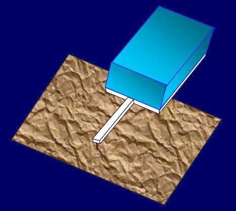
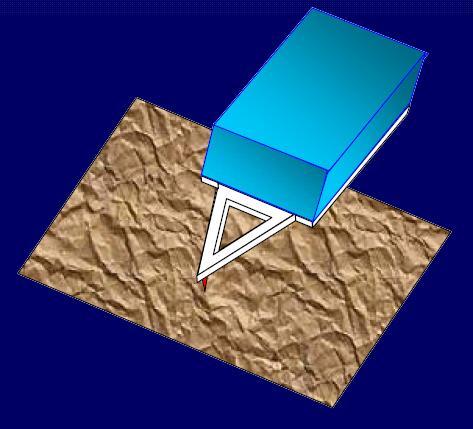
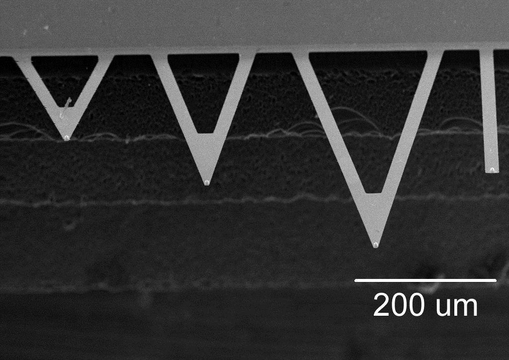
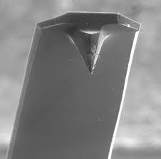
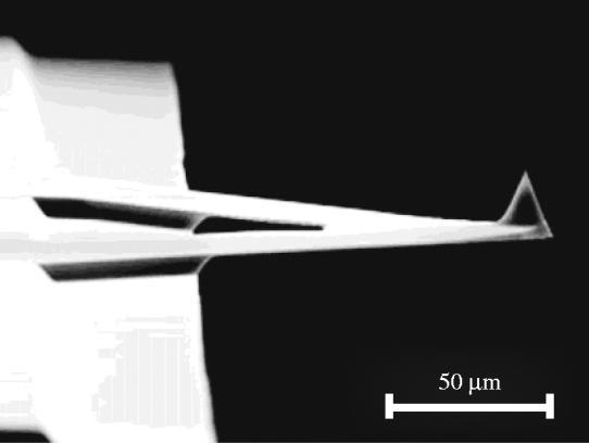
SUPPLEMENTARY NOTES Supplementary Note 1: Fabrication of Scanning Thermal Microscopy Probes
 SUPPLEMENTARY NOTES Supplementary Note 1: Fabrication of Scanning Thermal Microscopy Probes Fabrication of the scanning thermal microscopy (SThM) probes is summarized in Supplementary Fig. 1 and proceeds
672 Advanced Solid State Physics. Scanning Tunneling Microscopy
 672 Advanced Solid State Physics Scanning Tunneling Microscopy Biao Hu Outline: 1. Introduction to STM 2. STM principle & working modes 3. STM application & extension 4. STM in our group 1. Introduction
From nanophysics research labs to cell phones. Dr. András Halbritter Department of Physics associate professor
 From nanophysics research labs to cell phones Dr. András Halbritter Department of Physics associate professor Curriculum Vitae Birth: 1976. High-school graduation: 1994. Master degree: 1999. PhD: 2003.
2) Atom manipulation. Xe / Ni(110) Model: Experiment:
 Atom manipulation. Xe / Ni(110) Model: Experiment:") 2) Atom manipulation D. Eigler & E. Schweizer, Nature 344, 524 (1990) Xe / Ni(110) Model: Experiment: G.Meyer, et al. Applied Physics A 68, 125 (1999) First the tip is approached close to the adsorbate
2) Atom manipulation D. Eigler & E. Schweizer, Nature 344, 524 (1990) Xe / Ni(110) Model: Experiment: G.Meyer, et al. Applied Physics A 68, 125 (1999) First the tip is approached close to the adsorbate
Microscopical and Microanalytical Methods (NANO3)
") Microscopical and Microanalytical Methods (NANO3) 06.11.15 10:15-12:00 Introduction - SPM methods 13.11.15 10:15-12:00 STM 20.11.15 10:15-12:00 STS Erik Zupanič erik.zupanic@ijs.si stm.ijs.si 27.11.15
Microscopical and Microanalytical Methods (NANO3) 06.11.15 10:15-12:00 Introduction - SPM methods 13.11.15 10:15-12:00 STM 20.11.15 10:15-12:00 STS Erik Zupanič erik.zupanic@ijs.si stm.ijs.si 27.11.15
Visualization of Nanoscale Components Using Low Cost AFMs Part 2. Dr. Salahuddin Qazi
 Visualization of Nanoscale Components Using Low Cost AFMs Part 2 Dr. Salahuddin Qazi State University of New York Institute of Technology Utica, New York. Outline Introduction Visualization by Phase Imaging
Clark Atlanta University Center for Surface Chemistry and Catalysis Instrument Capabilities
 Center for Surface Chemistry and Catalysis Instrument Capabilities For information contact: Dr. Eric Mintz Research Center for Science and Technology Clark Atlanta University Atlanta, Georgia 30314 Phone:
CHARACTERIZATION of NANOMATERIALS KHP
 CHARACTERIZATION of NANOMATERIALS Overview of the most common nanocharacterization techniques MAIN CHARACTERIZATION TECHNIQUES: 1.Transmission Electron Microscope (TEM) 2. Scanning Electron Microscope
SUPPLEMENTARY INFORMATION
 1. Supplementary Methods Characterization of AFM resolution We employed amplitude-modulation AFM in non-contact mode to characterize the topography of the graphene samples. The measurements were performed
Scanning Tunneling Microscopy and its Application
 Chunli Bai Scanning Tunneling Microscopy and its Application With 181 Figures SHANGHAI SCIENTIFIC & TECHNICAL PUBLISHERS Jpl Springer Contents 1. Introduction 1 1.1 Advantages of STM Compared with Other
Seminars in Nanosystems - I
 Seminars in Nanosystems - I Winter Semester 2011/2012 Dr. Emanuela Margapoti Emanuela.Margapoti@wsi.tum.de Dr. Gregor Koblmüller Gregor.Koblmueller@wsi.tum.de Seminar Room at ZNN 1 floor Topics of the
Point mass approximation. Rigid beam mechanics. spring constant k N effective mass m e. Simple Harmonic Motion.. m e z = - k N z
 Free end Rigid beam mechanics Fixed end think of cantilever as a mass on a spring Point mass approximation z F Hooke s law k N = F / z This is beam mechanics, standard in engineering textbooks. For a rectangular
Infrared Spectroscopy
 Infrared Spectroscopy IR Spectroscopy Used to identify organic compounds IR spectroscopy provides a 100% identification if the spectrum is matched. If not, IR at least provides information about the types
CNPEM Laboratório de Ciência de Superfícies
 Investigating electrical charged samples by scanning probe microscopy: the influence to magnetic force microscopy and atomic force microscopy phase images. Carlos A. R. Costa, 1 Evandro M. Lanzoni, 1 Maria
Supporting Information
 Supporting Information Analysis Method for Quantifying the Morphology of Nanotube Networks Dusan Vobornik*, Shan Zou and Gregory P. Lopinski Measurement Science and Standards, National Research Council
Review. Surfaces of Biomaterials. Characterization. Surface sensitivity
 Surfaces of Biomaterials Three lectures: 1.23.05 Surface Properties of Biomaterials 1.25.05 Surface Characterization 1.27.05 Surface and Protein Interactions Review Bulk Materials are described by: Chemical
Chapter 12. Nanometrology. Oxford University Press All rights reserved.
 Chapter 12 Nanometrology Introduction Nanometrology is the science of measurement at the nanoscale level. Figure illustrates where nanoscale stands in relation to a meter and sub divisions of meter. Nanometrology
Reducing dimension. Crystalline structures
 Reducing dimension 2D surfaces, interfaces and quantum wells 1D carbon nanotubes, quantum wires and conducting polymers 0D nanocrystals, nanoparticles, lithographically patterned quantum dots Crystalline
Vibrational Spectroscopies. C-874 University of Delaware
 Vibrational Spectroscopies C-874 University of Delaware Vibrational Spectroscopies..everything that living things do can be understood in terms of the jigglings and wigglings of atoms.. R. P. Feymann Vibrational
instruments anasys Nanoscale Thermal Analysis Craig Prater, CTO Research Challenges for Nanomanufacturing Systems Februay th, 2008
 Nanoscale Thermal Analysis Craig Prater, CTO Research Challenges for Nanomanufacturing Systems Februay 11-12 th, 2008 Motivations Nanomanufacturing needs characterization for research, product development
Scanning tunneling microscopy
 IFM The Department of Physics, Chemistry and Biology Lab 72 in TFFM08 Scanning tunneling microscopy NAME PERS. - NUMBER DATE APPROVED Rev. Dec 2006 Ivy Razado Aug 2014 Tuomas Hänninen Contents 1 Introduction
Supporting Information
 Supporting Information Spatially-resolved imaging on photocarrier generations and band alignments at perovskite/pbi2 hetero-interfaces of perovskite solar cells by light-modulated scanning tunneling microscopy
Nitride HFETs applications: Conductance DLTS
 Nitride HFETs applications: Conductance DLTS The capacitance DLTS cannot be used for device trap profiling as the capacitance for the gate will be very small Conductance DLTS is similar to capacitance
Bonds and Wavefunctions. Module α-1: Visualizing Electron Wavefunctions Using Scanning Tunneling Microscopy Instructor: Silvija Gradečak
 3.014 Materials Laboratory December 8 th 13 th, 2006 Lab week 4 Bonds and Wavefunctions Module α-1: Visualizing Electron Wavefunctions Using Scanning Tunneling Microscopy Instructor: Silvija Gradečak OBJECTIVES
nano-ta: Nano Thermal Analysis
 nano-ta: Nano Thermal Analysis Application Note #1 Failure Analysis - Identification of Particles in a Polymer Film Author: David Grandy Ph.D. Introduction Nano-TA is a local thermal analysis technique
Spectroscopies for Unoccupied States = Electrons
 Spectroscopies for Unoccupied States = Electrons Photoemission 1 Hole Inverse Photoemission 1 Electron Tunneling Spectroscopy 1 Electron/Hole Emission 1 Hole Absorption Will be discussed with core levels