Expanding Characterization of Materials with Kelvin Force Microscopy
|
|
|
- Harold Hood
- 5 years ago
- Views:
Transcription


1 Expanding Characterization of Materials with Kelvin Force Microscopy Sergei Magonov Page 1
2 Outline Introduction to Kelvin Force Microscopy Different KFM Modes and Their Practical Evaluation Applications of Kelvin Force Microscopy Metals and Semiconductors Molecular Self-Assemblies Conclusions Page Group/Presentation Title Agilent Restricted Month ##, X
3 Atomic Force Microscopy/Scanning Force Microscopy High-Resolution/Low- i Local Mechanical Local Electromagnetic Other Properties: Force Profilometry Properties Properties Optical, Thermal, Air Vapors Liquid Vacuum High/Low Temperatures Local Electromagnetic Properties Force sensing Magnetic Force Microscopy, MFM Electric Force Microscopy, EFM: df/dz Kelvin Force Microscopy, KFM (SKPM) : surface potential, dc/dz Piezoresponse Force Microscopy, PFM Current sensing Conducting AFM, c-afm Scanning spreading resistance microscopy, SSRM Capacitance/Impedance sensing Scanning capacitance microscopy Scanning microwave microscopy Page 3 Group/Presentation Title Agilent Restricted Month ##, X
")


4 Kelvin Probe Technique (macroscopic method) Surface potential of semiconductor V s = ΔW f + V ox + φ s B. Laegel, M. D. Ayala, R. Schlaf APL, 5, 1. Page Group/Presentation Title Agilent Restricted Month ##, X


5 Metalized Probe Historical Pathway of AFM-based Electrostatic modes Electric force microscopy Contours of constant force gradient Back electrode Contours of constant force gradient An example of a cross-talk Y. Martin, D. A. Abraham, H. K. Wickramasinghe, Appl. Phys. Lett. 5, 113,19. J.E. Stern, B.D. Terris, H.J. Mamin, and D. Rugar, Appl. Phys. Lett. 53, 717, 19.
6 Electrostatic Force in Atomic Force Microscopy Metalized Probe Back electrode Responses at ω and ω can be used for detection of surface charge and capacitance/dielectric constant. KFM feedback is the nullifying the electrostatic t ti force at ω. J. M. R. Weaver and D. W. Abraham, J. Vac. Sci. Techn. 1991, B9, 1559 M. Nonnenmacher, M. P. O Boyle, H. K. Wickramasinghe, Appl. Phys. Lett. 5, 91, Electrostatic force at ω is proportional to dc/dz Solution: Problem: the AFM probe responds to all tip-sample forces! Single Pass the use of frequencies(ω mech, ω elec ) for probing mechanical and electrostatic tip-sample forces + operation in non-contact mode Y. Martin, D. A. Abraham, H. K. Wickramasinghe, Appl. Phys. Lett. 5, 113,19 Path Lift technique - the use of single frequency (ω mech ) with probing the electrostatic force in non-contact mode V. B. Elings, J. A. Gurley US Patent 5,3,97, 199. Page Month ##, X


7 Advanced Consideration of Electric Force Measurements with AFM Electrostatic energy and force J. Colchero, A. Gil, and A. M. Baro Phys Rev B (1) 53 Total force F Spatial Resolution in KFM Cantilever Metal Surface Cone Metal Surface Apex Metal Surface Force gradient vs. Force!? S. Kitamura et al Appl. Surf. Sci., 157, Atomic-scale KFM resolution on crystals in UHV KFM-FM InSb KFM-FM KCl 15 nm U. Zerweck et al Phys. Rev. B 5, 71, 15 UHV KFM-Lift BR M. Zhao et al Nanotechnology, 19, 357 UHV FK F. Krok et al lphys. Rev. B, 77, nm KCl Au nm KFM-AM Page 7 Group/Presentation Title Agilent Restricted Month ##, X


 ω elec ω mech")


8 Kelvin Force Microscopy in AM-AM and AM-FM modes AM-AM AM-AM: the amplitude changes at ω elec reflect the electrostatic force variations. AM-FM: the electrostatic force gradient causes the phase shift at ω mech which is reflected in the amplitude of satellites. Amplitude-versus-Frequency (sketch) ω elec ω mech Heterodyne procedure ω mech ω elec ω mech + ω elec AM-FM Imaging in the intermittent contact! A Non-contact Intermittent contact UHV: L.Eng et al Phys. Rev. B 71 (5) 15 Z Page


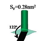
9 Conducting Probes for AFM-Based Electrical Modes SEM TEM Pt-coated Olympus probes 5 N/m, ~ 7 khz SEM SEM SEM images- courtesy of Maozi Liu (Agilent Labs) TEM image courtesy of Bernard Mesa (MicroStar Technologies) Page 9 Group/Presentation Title Agilent Restricted Month ##, X

 1 -(CH ) H")


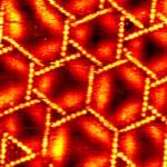
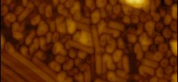
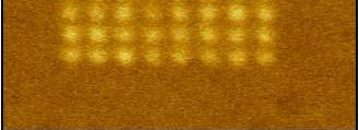
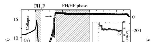
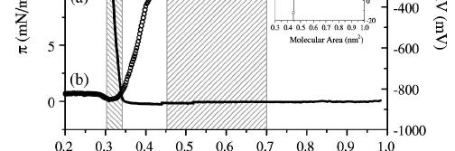
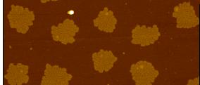
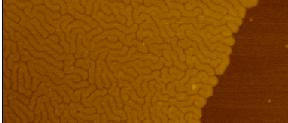
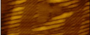
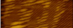
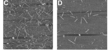
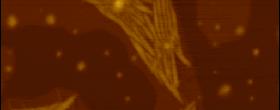
10 . nm Semifluorinated Alkanes: Self-Assembly in Thin Films F(CF ) 1 -(CH ) H F 1 H F(CF ) 1 -(CH ) H F 1 H nm -CF -δ δ CH +δ -. nm nm 9.9 nm. nm F 1 H F 1 H F 1 H F 1 H 1 μm nm F1H: Perfluorodecalin li vapor 5 nm 1 μm Substrates: Si, mica, graphite Solvent: perfluorodecalin A. Mourran et al Langmuir 5, 1, 3

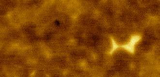
11 Self-Assemblies of Semifluorinated Alkane F 1 H on Si: EFM, KFM and dc/dz Topography X-component (5kHz), KFM servo off AM-FM Electric Force Microscopy, EFM 1. μm Surface Potential (5kHz) KFM servo on 1. μm dc/dz (1kHz) Surface Potential (5kHz) Page μm 1. μm


 (Y)")
12 Comparison of AM-AM and AM-FM modes in study of F 1 H self-assemblies Topography Surface Potential, AM-FM (Phase) Surface Potential, AM-AM Surface Potential, AM-FM (Phase) Surface Potential, AM-AM Surface Potential, AM-FM (Y) Surface Potential, AM-FM (Y)
13 Spatial resolution of KFM (AM-FM) in the Intermittent Contact: F 1 H on HOPG Topography Surface Potential Surface Potential Topography F 1 H F 1 H 1 nm F 1 H 1 μm 1 μm 5 nm 3 μm Topography Surface Potential Surface Potential Surface Potential.1V nm 1 μm 1 μm nm 3 μm


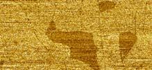


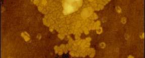
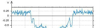
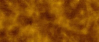
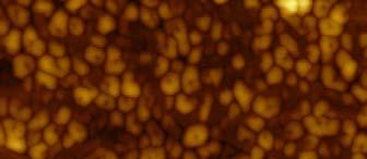
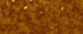
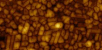
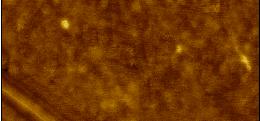
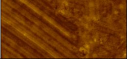
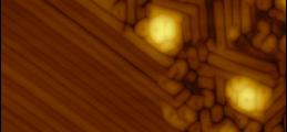
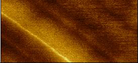
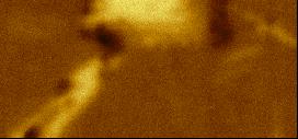
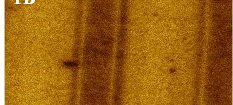
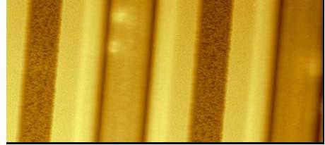
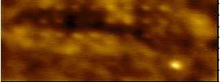
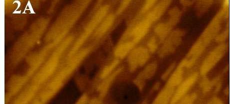
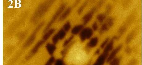
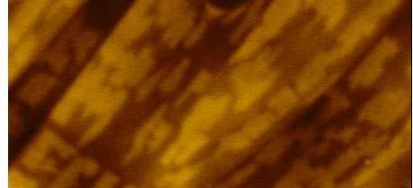
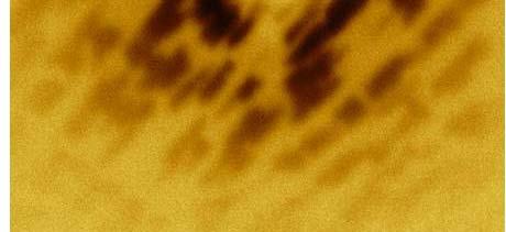
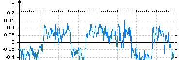
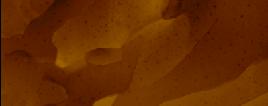
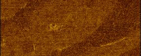
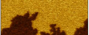
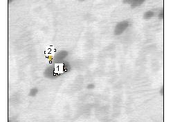
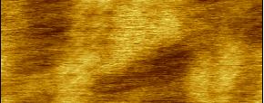
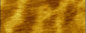
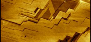
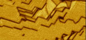
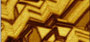
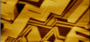
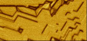
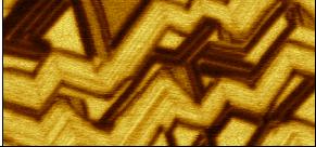
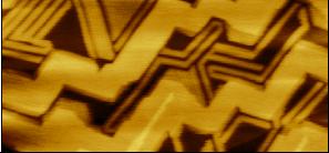
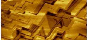
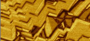
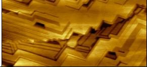
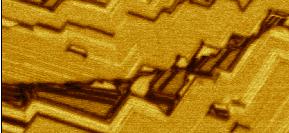
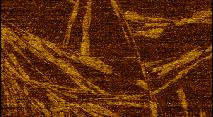
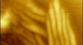
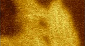
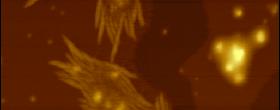
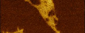
14 HOPG Topography Kelvin Force Microscopy of Substrates: Au (111) & HOPG µm Topography Au (111) µm Phase µm Surface Potential µ h hours after cleavage +15 min 1 1 µm +3 min +5 min µ + min +75 min Surface Potential ti µm Phase m Page 1 Group/Presentation Title Agilent Restricted Month ##, X

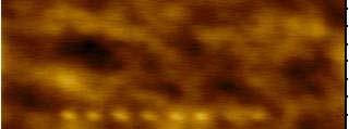

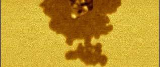
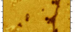
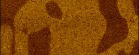
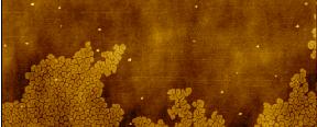
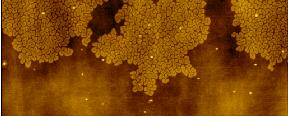
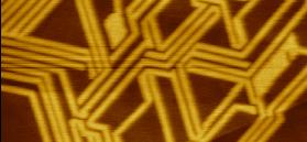
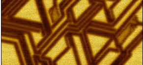
15 Kelvin Force Microscopy & Compositional Imaging of Material Heterogeneities SiGe PMMA topography surface potential topography surface potential 5 μm 5 μm μm μm TPV (polypropylene, EPDM, carbon black) C H 1 topography surface potential topography surface potential 5 μm 5 μm μm μm Page 15 Month ##, X
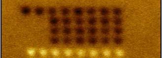
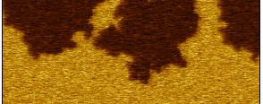
16 Monitoring Changes of Soldering Materials: 5%Bi-%Sn Alloy 1 hr after preparation Bi.eV Sn. ev topography surface potential μm μm 15 hr after preparation topography surface potential μm μm Page 1
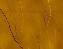
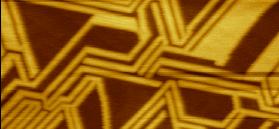
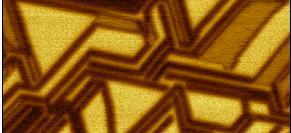
17 KFM of Semifluorinated Alkane F 1 H Assemblies on Si Substrate Topography Surface Potential Zmean() Zmean(1).73 V Zmean() Zmean(1).757 V F(CF ) 1 -(CH ) H -CF -δ +δ CH nm. nm A. El Abed et al PRE, 5, 513

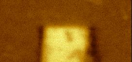
18 KFM of Semifluorinated Alkane F 1 H Assemblies on Mica Substrate Topography Surface Potential Zmean() Zmean(1) 1.51 V μ=3.1d μm 3 μm Topography Surface Potential A. Mourran et al Langmuir 5, 1, 3 ( ϕ si ϕtip ) μ V = + Zmean() Zmean(1)1. V e A ε ε ( ϕ si ϕtip ) CPD = e V = CPD Volts 1.5 μm 1.5 μm
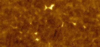
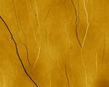
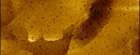
19 KFM of Semifluorinated Alkane F 1 H Assemblies on HOPG substrate Topography Phase Surface Potential Zmean() Zmean(1).73 V 1 7 nm 7 nm Topography nm Surface Potential 1 9. nm nm nm


 V.")
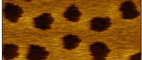
20 KFM of Semifluorinated Alkane F 1 H Assemblies on Si substrate: Humid Air Spreading of self-assemblies and conversion from spirals to toroids Topography Topography Topography Topography 1 μm 1 μm 3 μm 1 μm 1 1 Topography Topography Surface Potential Zmean() Zmean(1) V. nm nm nm


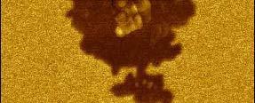
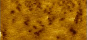
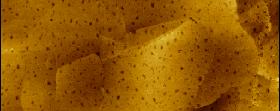
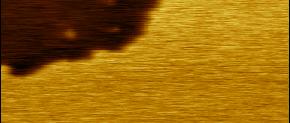
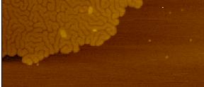
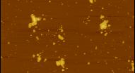
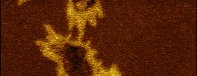
21 Monitoring of Sublimation of F 1 H Self-Assemblies on Mica Topography 115 min Topography 1 min Topography min Topography min nm nm nm nm Topography 55 min Surface Potential Topography Surface Potential nm nm Page 1 Month ##, X

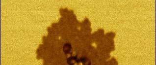
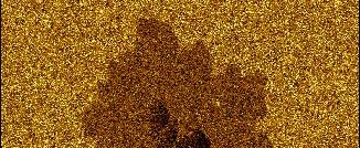
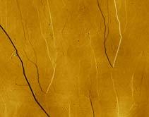
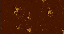
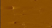
22 Monitoring of Sublimation of F 1 H Self-Assemblies on Graphite Topography Surface Potential Topography Surface Potential μm 1. μm 1 μm 1 μm Topography Surface Potential Topography Surface Potential 1. μm 1. μm 1 μm 1 μm Page Group/Presentation Title Agilent Restricted Month ##, X


 self-assemblies does")


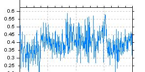
23 Monitoring of Sublimation of F 1 H Self-Assemblies on Graphite Topography Surface Potential Topography Surface Potential 7 nm 7 nm Topography Surface Potential 5 nm 5 nm Surface potential of FnHm (n=1, 1; m =, 1, 1, ) self-assemblies does not depend on the molecular length being determined primarily by molecular dipoles of -CF -δ CH +δ -, -CF 3 and CH 3 groups and their orientation. Page 3 Group/Presentation Title Agilent Restricted Month ##, X


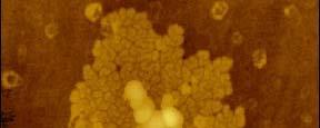
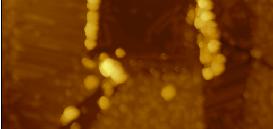
24 Z. Tang, N. A. Kotov, M. Giersig Science, 97, 37 Self-Assembly of CdTe Nanoparticles into Nanowires After spincast in 9% humidity topography phase surface potential 5 μm 5 μm 5 μm topography phase surface potential Sample in 9% humidity after night 5 μm 5 μm 5 μm topography phase surface potential High luminescence quantum yields Dried Page
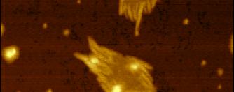
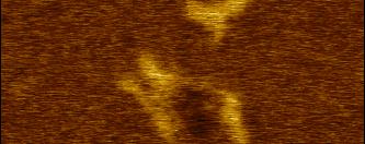
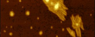
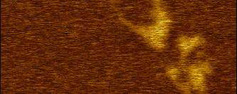

25 Self-Assembly of CdTe Nanoparticles into Nanowires topography surface potential topography surface potential 3 nm 3 nm. μm topography (1 min later). μm surface potential S. Shanbhag, N. Kotov, J. Phys. Chem. B, Let, 11, 111 Cubic NCs: ZnS, CdS, ZnSe, PbSe, and CdTe μ Page 5 1. μm 1. μm
26 Conclusions Expansion of AFM applications strongly depends on practical implementation of a combination of high-resolution capabilities with mapping of local properties in broad range of environments. Here the unique capabilities of KFM as the characterization technique down to the sub-1 nm scale were demonstrated on a number of materials. The progress of AFM-based local electric (as well as mechanical) studies is based on use of multiple frequencies and a broader frequency range. Analysis of multifrequency responses leads to more sensitive and high-resolution mapping of these properties. Nanotechnology 1 (7) 55 R W Stark, N Naujoks and A Stemmer The multifrequency approach in AFM and related techniques requires definite efforts towards optimization of experiments, which include a choice of rational detection schemes, an appropriate choice of probes and imaging conditions. There is no doubts that the payoff will be quite valuable and unique information about materials, their properties and behavior will be discovered. Page Group/Presentation Title Agilent Restricted Month ##, X
27 Acknowledgements John Alexander (Agilent Technologies) - for everyday cooperation on AFM developments and applications Martin Moeller (RWTH--DWI, Aachen, Germany) Nicholas Kotov (University of Michigan, Ann Arbor, MI) Page 7 Group/Presentation Title Agilent Restricted Month ##, X
High-resolution Characterization of Organic Ultrathin Films Using Atomic Force Microscopy
 High-resolution Characterization of Organic Ultrathin Films Using Atomic Force Microscopy Jing-jiang Yu Nanotechnology Measurements Division Agilent Technologies, Inc. Atomic Force Microscopy High-Resolution
Single-Pass Measurements in Atomic Force Microscopy: Kelvin Force Microscopy and Local Dielectric Studies
 Single-Pass Measurements in Atomic Force Microscopy: Kelvin Force Microscopy and Local Dielectric Studies NT-MDT Development Inc. 416 W. Warner Rd. Tempe AZ USA ABSTRACT Advanced studies of surface potential
Electrostatic Force Microscopy (EFM)
") 6 Electrostatic Force Microscopy (EFM) Masakazu Nakamura and Hirofumi Yamada 1 Department of Electronics and Mechanical Engineering, Faculty of Engineering, Chiba University, 1-33 Yayoi-cho, Inage-ku,
6 Electrostatic Force Microscopy (EFM) Masakazu Nakamura and Hirofumi Yamada 1 Department of Electronics and Mechanical Engineering, Faculty of Engineering, Chiba University, 1-33 Yayoi-cho, Inage-ku,
Single-Pass Measurements in Atomic Force Microscopy: Kelvin Probe Force Microscopy and Local Dielectric Studies
 Application Note 08 Single-Pass Measurements in Atomic Force Microscopy: Kelvin Probe Force Microscopy and Local Dielectric Studies Sergei Magonov, NT-MDT Development Inc. 46 W. Warner Rd. Tempe AZ USA
BDS2016 Tutorials: Local Dielectric Spectroscopy by Scanning Probes
 BDS2016 Tutorials: Local Dielectric Spectroscopy by Scanning Probes Massimiliano Labardi CNR Institute for Physico-Chemical Processes (IPCF) Pisa (Italy) OUTLINE Broadband Dielectric Spectroscopy (BDS):
Keysight Technologies Advanced Atomic Force Microscopy: Exploring Measurements of Local Electric Properties. Application Note
 Keysight Technologies Advanced Atomic Force Microscopy: Exploring Measurements of Local Electric Properties Application Note Introduction In the past two decades Atomic Force Microscopy (AFM) 1 has been
Scanning Probe Microscopy (SPM)
") Scanning Probe Microscopy (SPM) Scanning Tunneling Microscopy (STM) --- G. Binnig, H. Rohrer et al, (1982) Near-Field Scanning Optical Microscopy (NSOM) --- D. W. Pohl (1982) Atomic Force Microscopy (AFM)
Scanning Probe Microscopy (SPM) Scanning Tunneling Microscopy (STM) --- G. Binnig, H. Rohrer et al, (1982) Near-Field Scanning Optical Microscopy (NSOM) --- D. W. Pohl (1982) Atomic Force Microscopy (AFM)
Principle of Electrostatic Force Microscopy and Applications. Thierry Mélin.
 Principle of Electrostatic Force Microscopy and Applications Thierry Mélin thierry.melin@univ-lille1.fr ANF-DFRT CEA Leti, Dec 1 st 2016 I Introduction II Electrostatic Force Microscopy (EFM) III Kelvin
Measurement of hardness, surface potential, and charge distribution with dynamic contact mode electrostatic force microscope
 REVIEW OF SCIENTIFIC INSTRUMENTS VOLUME 70, NUMBER 3 MARCH 1999 Measurement of hardness, surface potential, and charge distribution with dynamic contact mode electrostatic force microscope J. W. Hong,
Dopant Concentration Measurements by Scanning Force Microscopy
 73.40L Scanning Microsc. Microanal. Microstruct. 551 Classification Physics Abstracts - - 61.16P 73.00 Dopant Concentration Measurements by Scanning Force Microscopy via p-n Junctions Stray Fields Jacopo
Application Note High Definiton Kelvin Force Microscopy BIMODAL HD-KFM
 Application Note High Definiton Kelvin Force Microscopy BIMODAL HD-KFM INTRODUCTION Since the invention of the Atomic Force Microscope in 1986, many different measurement modes have been proposed to characterize
realistic nanostructured systems
 Electrostatic force microscopy and potentiometry of realistic nanostructured systems M. Lucchesi (,), G. Privitera (), M. Labardi () *, D. Prevosto (), S. Capaccioli (,), P. Pingue (3) Dipartimento di
Other SPM Techniques. Scanning Probe Microscopy HT10
 Other SPM Techniques Scanning Near-Field Optical Microscopy (SNOM) Scanning Capacitance Microscopy (SCM) Scanning Spreading Resistance Microscopy (SSRM) Multiprobe techniques Electrostatic Force Microscopy,
Module 26: Atomic Force Microscopy. Lecture 40: Atomic Force Microscopy 3: Additional Modes of AFM
 Module 26: Atomic Force Microscopy Lecture 40: Atomic Force Microscopy 3: Additional Modes of AFM 1 The AFM apart from generating the information about the topography of the sample features can be used
Agilent Technologies. Scanning Microwave Microscopy (SMM)
") Agilent Technologies Scanning Microwave Microscopy (SMM) Expanding Impedance Measurements to the Nanoscale: Coupling the Power of Scanning Probe Microscopy with the PNA Presented by: Craig Wall PhD Product
Agilent Technologies Scanning Microwave Microscopy (SMM) Expanding Impedance Measurements to the Nanoscale: Coupling the Power of Scanning Probe Microscopy with the PNA Presented by: Craig Wall PhD Product
Practical aspects of Kelvin probe force microscopy
 REVIEW OF SCIENTIFIC INSTRUMENTS VOLUME 70, NUMBER 3 MARCH 1999 Practical aspects of Kelvin probe force microscopy H. O. Jacobs, H. F. Knapp, and A. Stemmer a) Swiss Federal Institute of Technology, Nanotechnology
Nanostructure. Materials Growth Characterization Fabrication. More see Waser, chapter 2
 Nanostructure Materials Growth Characterization Fabrication More see Waser, chapter 2 Materials growth - deposition deposition gas solid Physical Vapor Deposition Chemical Vapor Deposition Physical Vapor
Introduction to Scanning Probe Microscopy Zhe Fei
 Introduction to Scanning Probe Microscopy Zhe Fei Phys 590B, Apr. 2019 1 Outline Part 1 SPM Overview Part 2 Scanning tunneling microscopy Part 3 Atomic force microscopy Part 4 Electric & Magnetic force
Supplementary Information for. Effect of Ag nanoparticle concentration on the electrical and
 Supplementary Information for Effect of Ag nanoparticle concentration on the electrical and ferroelectric properties of Ag/P(VDF-TrFE) composite films Haemin Paik 1,2, Yoon-Young Choi 3, Seungbum Hong
Program Operacyjny Kapitał Ludzki SCANNING PROBE TECHNIQUES - INTRODUCTION
 Program Operacyjny Kapitał Ludzki SCANNING PROBE TECHNIQUES - INTRODUCTION Peter Liljeroth Department of Applied Physics, Aalto University School of Science peter.liljeroth@aalto.fi Projekt współfinansowany
Noncontact-AFM (nc-afm)
") Noncontact-AFM (nc-afm) Quantitative understanding of nc-afm A attractive interaction Δf Resonance frequency: f 0 Width of resonance curve (FWHM): Γ Γ+ΔΓ Γ Q-factor: Q π f Γ = 0 f 0 f Conservative forces
Noncontact-AFM (nc-afm) Quantitative understanding of nc-afm A attractive interaction Δf Resonance frequency: f 0 Width of resonance curve (FWHM): Γ Γ+ΔΓ Γ Q-factor: Q π f Γ = 0 f 0 f Conservative forces
Scanning Tunneling Microscopy
 Scanning Tunneling Microscopy Scanning Direction References: Classical Tunneling Quantum Mechanics Tunneling current Tunneling current I t I t (V/d)exp(-Aφ 1/2 d) A = 1.025 (ev) -1/2 Å -1 I t = 10 pa~10na
Intermittent-Contact Mode Force Microscopy & Electrostatic Force Microscopy (EFM)
") WORKSHOP Nanoscience on the Tip Intermittent-Contact Mode Force Microscopy & Electrostatic Force Microscopy (EFM) Table of Contents: 1. Motivation... 1. Simple Harmonic Motion... 1 3. AC-Mode Imaging...
WORKSHOP Nanoscience on the Tip Intermittent-Contact Mode Force Microscopy & Electrostatic Force Microscopy (EFM) Table of Contents: 1. Motivation... 1. Simple Harmonic Motion... 1 3. AC-Mode Imaging...
Chapter 2 Experimental Technique and Working Modes
 Chapter 2 Experimental Technique and Working Modes S. Sadewasser Abstract Kelvin probe force microscopy is a scanning probe microscopy technique providing the capability to image the local surface potential
Scanning Probe Microscopy (SPM)
") http://ww2.sljus.lu.se/staff/rainer/spm.htm Scanning Probe Microscopy (FYST42 / FAFN30) Scanning Probe Microscopy (SPM) overview & general principles March 23 th, 2018 Jan Knudsen, room K522, jan.knudsen@sljus.lu.se
http://ww2.sljus.lu.se/staff/rainer/spm.htm Scanning Probe Microscopy (FYST42 / FAFN30) Scanning Probe Microscopy (SPM) overview & general principles March 23 th, 2018 Jan Knudsen, room K522, jan.knudsen@sljus.lu.se
CNPEM Laboratório de Ciência de Superfícies
 Investigating electrical charged samples by scanning probe microscopy: the influence to magnetic force microscopy and atomic force microscopy phase images. Carlos A. R. Costa, 1 Evandro M. Lanzoni, 1 Maria
Magnetic ordering in two-dimensional. nanoparticle assemblies
 Magnetic ordering in two-dimensional nanoparticle assemblies Pedro Zeijlmans van Emmichoven Faculty of Science, Utrecht University Leiden, June 18 th, 2007 Collaborators Mirela Georgescu Mark Klokkenburg
Electrical Characterization with SPM Application Modules
 Electrical Characterization with SPM Application Modules Metrology, Characterization, Failure Analysis: Data Storage Magnetoresistive (MR) read-write heads Semiconductor Transistors Interconnect Ferroelectric
AFM Imaging In Liquids. W. Travis Johnson PhD Agilent Technologies Nanomeasurements Division
 AFM Imaging In Liquids W. Travis Johnson PhD Agilent Technologies Nanomeasurements Division Imaging Techniques: Scales Proteins 10 nm Bacteria 1μm Red Blood Cell 5μm Human Hair 75μm Si Atom Spacing 0.4nm
Atomic Force Microscopy imaging and beyond
 Atomic Force Microscopy imaging and beyond Arif Mumtaz Magnetism and Magnetic Materials Group Department of Physics, QAU Coworkers: Prof. Dr. S.K.Hasanain M. Tariq Khan Alam Imaging and beyond Scanning
Studies of the Properties of Designed Nanoparticles Using Atomic Force Microscopy
 Louisiana State University LSU Digital Commons LSU Doctoral Dissertations Graduate School 2016 Studies of the Properties of Designed Nanoparticles Using Atomic Force Microscopy Steve Matthew Deese Louisiana
Basic Laboratory. Materials Science and Engineering. Atomic Force Microscopy (AFM)
") Basic Laboratory Materials Science and Engineering Atomic Force Microscopy (AFM) M108 Stand: 20.10.2015 Aim: Presentation of an application of the AFM for studying surface morphology. Inhalt 1.Introduction...
Basic Laboratory Materials Science and Engineering Atomic Force Microscopy (AFM) M108 Stand: 20.10.2015 Aim: Presentation of an application of the AFM for studying surface morphology. Inhalt 1.Introduction...
STM: Scanning Tunneling Microscope
 STM: Scanning Tunneling Microscope Basic idea STM working principle Schematic representation of the sample-tip tunnel barrier Assume tip and sample described by two infinite plate electrodes Φ t +Φ s =
Scanning Force Microscopy II
 Scanning Force Microscopy II Measurement modes Magnetic force microscopy Artifacts Lars Johansson 1 SFM - Forces Chemical forces (short range) Van der Waals forces Electrostatic forces (long range) Capillary
Supporting Information. Real-time nanoscale open-circuit voltage dynamics of perovskite solar cells
 Supporting Information Real-time nanoscale open-circuit voltage dynamics of perovskite solar cells Joseph L. Garrett 1,2, Elizabeth M. Tennyson 2,3,Miao Hu 4, Jinsong Huang 4, Jeremy N. Munday 2,5*, Marina
Supplementary Information. Characterization of nanoscale temperature fields during electromigration of nanowires
 Supplementary Information Characterization of nanoscale temperature fields during electromigration of nanowires Wonho Jeong,, Kyeongtae Kim,, *, Youngsang Kim,, Woochul Lee,, *, Pramod Reddy Department
Imaging Methods: Scanning Force Microscopy (SFM / AFM)
") Imaging Methods: Scanning Force Microscopy (SFM / AFM) The atomic force microscope (AFM) probes the surface of a sample with a sharp tip, a couple of microns long and often less than 100 Å in diameter.
Imaging Methods: Scanning Force Microscopy (SFM / AFM) The atomic force microscope (AFM) probes the surface of a sample with a sharp tip, a couple of microns long and often less than 100 Å in diameter.
AFM: Atomic Force Microscopy II
 AM: Atomic orce Microscopy II Jan Knudsen The MAX IV laboratory & Division of synchrotron radiation research K522-523 (Sljus) 4 th of May, 2018 http://www.sljus.lu.se/staff/rainer/spm.htm Last time: The
Instrumentation and Operation
 Instrumentation and Operation 1 STM Instrumentation COMPONENTS sharp metal tip scanning system and control electronics feedback electronics (keeps tunneling current constant) image processing system data
Magnetic Force Microscopy (MFM) F = µ o (m )H
 F = µ o (m )H") Magnetic Force Microscopy (MFM) F = µ o (m )H 1. MFM is based on the use of a ferromagnetic tip as a local field sensor. Magnetic interaction between the tip and the surface results in a force acting on
Magnetic Force Microscopy (MFM) F = µ o (m )H 1. MFM is based on the use of a ferromagnetic tip as a local field sensor. Magnetic interaction between the tip and the surface results in a force acting on
The dielectric response of Molecular Wires
 The dielectric response of Molecular Wires Julio Gómez Laboratorio de Nuevas Microscopías. Departamento de Física de la Materia Condensada C-III Universidad Autónoma de Madrid Nanowires overview Breakjuncti
Lecture 12: Biomaterials Characterization in Aqueous Environments
 3.051J/20.340J 1 Lecture 12: Biomaterials Characterization in Aqueous Environments High vacuum techniques are important tools for characterizing surface composition, but do not yield information on surface
Today s SPM in Nanotechnology
 Today s SPM in Nanotechnology An introduction for Advanced Applications Qun (Allen) Gu, Ph.D., AFM Scientist, Pacific Nanotechnology IEEE Bay Area Nanotechnology Council, August, 2007 8/17/2015 1 Content
NIS: what can it be used for?
 AFM @ NIS: what can it be used for? Chiara Manfredotti 011 670 8382/8388/7879 chiara.manfredotti@to.infn.it Skype: khiaram 1 AFM: block scheme In an Atomic Force Microscope (AFM) a micrometric tip attached
Figure S1 TEM image of nanoparticles, showing the hexagonal shape of the particles.
 Electronic Supplementary Material (ESI) for Journal of Materials Chemistry A. This journal is The Royal Society of Chemistry 2014 Electronic Supplementary Information Au@Poly(acrylic acid) Plasmons and
Outline Scanning Probe Microscope (SPM)
") AFM Outline Scanning Probe Microscope (SPM) A family of microscopy forms where a sharp probe is scanned across a surface and some tip/sample interactions are monitored Scanning Tunneling Microscopy (STM)
AFM Outline Scanning Probe Microscope (SPM) A family of microscopy forms where a sharp probe is scanned across a surface and some tip/sample interactions are monitored Scanning Tunneling Microscopy (STM)
Exploring Materials with AFM-based Electrostatic Modes
 Application Note 84 Exploring Materials with AFM-based Electrostatic Modes Electrostatic Force Microscopy: Experiments and quantitative analysis Local surface potential studies with single-pass Kelvin
Force-distance studies with piezoelectric tuning forks below 4.2K
 submitted to APPLIED SURFACE SCIENCE nc-afm 99, Pontresina Force-distance studies with piezoelectric tuning forks below 4.2K J. Rychen, T. Ihn, P. Studerus, A. Herrmann, K. Ensslin Solid State Physics
Application of electrostatic force microscopy in nanosystem diagnostics
 Materials Science, Vol., No. 3, 003 Application of electrostatic force microscopy in nanosystem diagnostics TEODOR P. GOTSZALK *, PIOTR GRABIEC, IVO W. RANGELOW 3 Fulty of Microsystem Electronics and Photonics,
Electrochemically Exfoliated Graphene as Solution-Processable, Highly-Conductive Electrodes for Organic Electronics
 Supporting Information Electrochemically Exfoliated Graphene as Solution-Processable, Highly-Conductive Electrodes for Organic Electronics Khaled Parvez, Rongjin Li, Sreenivasa Reddy Puniredd, Yenny Hernandez,
From nanophysics research labs to cell phones. Dr. András Halbritter Department of Physics associate professor
 From nanophysics research labs to cell phones Dr. András Halbritter Department of Physics associate professor Curriculum Vitae Birth: 1976. High-school graduation: 1994. Master degree: 1999. PhD: 2003.
Scanning Probe Microscopy. L. J. Heyderman
 1 Scanning Probe Microscopy 2 Scanning Probe Microscopy If an atom was as large as a ping-pong ball......the tip would have the size of the Matterhorn! 3 Magnetic Force Microscopy Stray field interaction
Charge transfer between surfaces of two distinctly different. In Situ Quantitative Study of Nanoscale Triboelectrification and Patterning
 pubs.acs.org/nanolett In Situ Quantitative Study of Nanoscale Triboelectrification and Patterning Yu Sheng Zhou, Ying Liu, Guang Zhu, Zong-Hong Lin, Caofeng Pan, Qingshen Jing, and Zhong Lin Wang*,, School
Magnetic Nanowires inside. carbon nanotubes
 Leibniz Institute for Solid State and Materials Research IFW Dresden Magnetic Nanowires inside Carbon Nanotubes Magnetic force microscopy sensors using ironfilled carbon nanotubes Thomas Mühl Outline Introduction
Development of a nanostructural microwave probe based on GaAs
 Microsyst Technol (2008) 14:1021 1025 DOI 10.1007/s00542-007-0484-0 TECHNICAL PAPER Development of a nanostructural microwave probe based on GaAs Y. Ju Æ T. Kobayashi Æ H. Soyama Received: 18 June 2007
Scanning probe studies of the electrical activity at interfaces formed by silicon wafer direct bonding
 phys. stat. sol. (c) 4, No. 8, 893 897 (007) / DOI 10.100/pssc.00675481 Scanning probe studies of the electrical activity at interfaces formed by silicon wafer direct bonding M. Ratzke *, 1,, O. Vyvenko
Exploring Materials with AFM-based Electrostatic Modes
 Application Note 84 Exploring Materials with AFM-based Electrostatic Modes Electrostatic Force Microscopy: Experiments and quantitative analysis Local surface potential studies with single-pass Kelvin
Scattering-type near-field microscopy for nanoscale optical imaging
 Scattering-type near-field microscopy for nanoscale optical imaging Rainer Hillenbrand Nano-Photonics Group Max-Planck-Institut für Biochemie 82152 Martinsried, Germany Infrared light enables label-free
Fabrication at the nanoscale for nanophotonics
 Fabrication at the nanoscale for nanophotonics Ilya Sychugov, KTH Materials Physics, Kista silicon nanocrystal by electron beam induced deposition lithography Outline of basic nanofabrication methods Devices
Expanding Atomic Force Microscopy with HybriD Mode Imaging
 Application Note 087 Expanding Atomic Force Microscopy with HybriD Mode Imaging Enhanced visualization of nanoscale structures - one of remarkable features of the HybriD Mode. High-resolution mapping of
Reducing dimension. Crystalline structures
 Reducing dimension 2D surfaces, interfaces and quantum wells 1D carbon nanotubes, quantum wires and conducting polymers 0D nanocrystals, nanoparticles, lithographically patterned quantum dots Crystalline
Using the surface spontaneous depolarization field of ferroelectrics to direct the assembly of virus particles
 Appl. Phys. Lett. Vol 85, Issue 16, 3537 (2004) Using the surface spontaneous depolarization field of ferroelectrics to direct the assembly of virus particles Working Title: Directed assembly of biological
MSE640: Advances in Investigation of Intermolecular & Surface Forces
 MSE640: Advances in Investigation of Forces Course Title Advances in investigation of Intermolecular & surface forces Course Code MSE640 Credit Hours 3 Pre-requisites (if any) MSE507, MSE508 or equivalent
Fundamentals of Atomic Force Microscopy Part 2: Dynamic AFM Methods
 Fundamentals of tomic Force Microscopy Part 2: Dynamic FM Methods Week 2, Lecture 5 ttractive and repulsive regimes and phase contrast in amplitude modulation FM rvind Raman Mechanical Engineering Birck
Greg Andreev and Aravind Vijayaraghavan 9/27/13
 Mapping Graphene s surface potential with
Fabrication of ordered array at a nanoscopic level: context
 Fabrication of ordered array at a nanoscopic level: context Top-down method Bottom-up method Classical lithography techniques Fast processes Size limitations it ti E-beam techniques Small sizes Slow processes
Nitride HFETs applications: Conductance DLTS
 Nitride HFETs applications: Conductance DLTS The capacitance DLTS cannot be used for device trap profiling as the capacitance for the gate will be very small Conductance DLTS is similar to capacitance
The Liquid Metal Ion Source A Hot Ion Source. Jon Orloff Professor Emeritus, University of Maryland and FEI Company Hillsboro, Oregon
 The Liquid Metal Ion Source A Hot Ion Source Jon Orloff Professor Emeritus, University of Maryland and FEI Company Hillsboro, Oregon U.S. Northwest Pacific Coast 2 Introduction The main purpose of this
29: Nanotechnology. What is Nanotechnology? Properties Control and Understanding. Nanomaterials
 29: Nanotechnology What is Nanotechnology? Properties Control and Understanding Nanomaterials Making nanomaterials Seeing at the nanoscale Quantum Dots Carbon Nanotubes Biology at the Nanoscale Some Applications
PY5020 Nanoscience Scanning probe microscopy
 PY500 Nanoscience Scanning probe microscopy Outline Scanning tunnelling microscopy (STM) - Quantum tunnelling - STM tool - Main modes of STM Contact probes V bias Use the point probes to measure the local
SUPPLEMENTARY INFORMATION
 DOI: 10.1038/NCHEM.1332 Light triggered self-construction of supramolecular organic nanowires as metallic interconnects Vina Faramarzi 1,2, Frédéric Niess 1,3, Emilie Moulin 3, Mounir Maaloum 1,3, Jean-François
Scanning Nanoelectrochemistry and Nanoelectrical Liquid Imaging with Nanoelectrode Probe
 Scanning Nanoelectrochemistry and Nanoelectrical Liquid Imaging with Nanoelectrode Probe Teddy Huang, PhD Sr. Applications Scientist, Bruker Nano Surfaces, Teddy.Huang@Bruker.com Outline Overview Nanoelectrode
Fabrication and Domain Imaging of Iron Magnetic Nanowire Arrays
 Abstract #: 983 Program # MI+NS+TuA9 Fabrication and Domain Imaging of Iron Magnetic Nanowire Arrays D. A. Tulchinsky, M. H. Kelley, J. J. McClelland, R. Gupta, R. J. Celotta National Institute of Standards
Proceedings of SPIE, Micro- and Nanoelectronics -2003, Vol. 5401, pp (2003).
.") Proceedings of SPIE, Micro- and Nanoelectronics -2003, Vol. 5401, pp 555-560 (2003). Magnetic force microscopy of magnetization reversal of microstructures in situ in the external field of up to 2000Oe
Proceedings of SPIE, Micro- and Nanoelectronics -2003, Vol. 5401, pp 555-560 (2003). Magnetic force microscopy of magnetization reversal of microstructures in situ in the external field of up to 2000Oe
Scanning Probe Microscopy. Amanda MacMillan, Emmy Gebremichael, & John Shamblin Chem 243: Instrumental Analysis Dr. Robert Corn March 10, 2010
 Scanning Probe Microscopy Amanda MacMillan, Emmy Gebremichael, & John Shamblin Chem 243: Instrumental Analysis Dr. Robert Corn March 10, 2010 Scanning Probe Microscopy High-Resolution Surface Analysis
Contents. What is AFM? History Basic principles and devices Operating modes Application areas Advantages and disadvantages
 Contents What is AFM? History Basic principles and devices Operating modes Application areas Advantages and disadvantages Figure1: 2004 Seth Copen Goldstein What is AFM? A type of Scanning Probe Microscopy
Experimental methods in physics. Local probe microscopies I
 Experimental methods in physics Local probe microscopies I Scanning tunnelling microscopy (STM) Jean-Marc Bonard Academic year 09-10 1. Scanning Tunneling Microscopy 1.1. Introduction Image of surface
Introduction to Nanomechanics: Magnetic resonance imaging with nanomechanics
 Introduction to Nanomechanics: Magnetic resonance imaging with nanomechanics Martino Poggio Swiss Nanoscience Institute Department of Physics University of Basel Switzerland Nano I, Herbstsemester 2009
Magnetic Force Microscopy
 Magnetic Force Microscopy June 1, 1998 Kim Byung-Il Dept. of Physics Seoul National Univ. 6/19/1 1 Superconductivity Lab. Development of MFM Noncontact mode weak interaction magnetic, electric and attr.
SUPPLEMENTARY NOTES Supplementary Note 1: Fabrication of Scanning Thermal Microscopy Probes
 SUPPLEMENTARY NOTES Supplementary Note 1: Fabrication of Scanning Thermal Microscopy Probes Fabrication of the scanning thermal microscopy (SThM) probes is summarized in Supplementary Fig. 1 and proceeds
The needs and challenges of electrical measurements for micro/nanoelectronic devices.
 1 The needs and challenges of electrical measurements for micro/nanoelectronic devices. Brice Gautier N. Baboux, D. Albertini, S. Martin, W. Hourani, A. Grandfond Institut des Nanotechnologies de Lyon
Characterization of Materials with a Combined AFM/Raman Microscope
 Application Note 089 full Characterization of Materials with a Combined AFM/Raman Microscope Introducing a combined AFM/Raman instrument based on Raman Confocal microscope DXR (Thermo Fisher Scientific)
Imaging Polymer Morphology Using Atomic Force Microscopy
 Imaging Polymer Morphology Using Atomic Force Microscopy Russell J. Composto Materials Science and Engineering, and the Laboratory for Research on the Structure of Matter, University of Pennsylvania Agilent
ELECTRON MICROSCOPE UNIT
 ELECTRON MICROSCOPE Director: Prof Richard Tilley Associate Director: Dr Nicholas Ariotti Lab Manager: Ms Katie Levick Administrative Assistant: Mr Michael Zhi UNIT Basement Level: F10 Chemical Sciences
Magnetic force microscopy of signature erasure in magnetic recording media
 Magnetic force microscopy of signature erasure in magnetic recording media Hsia-Po V. Kuo and E.D. Dahlberg Department of Physics, University of Minnesota Minneapolis, MN 55455 Magnetic force microscope
Supplementary Figure S1. AFM images of GraNRs grown with standard growth process. Each of these pictures show GraNRs prepared independently,
 Supplementary Figure S1. AFM images of GraNRs grown with standard growth process. Each of these pictures show GraNRs prepared independently, suggesting that the results is reproducible. Supplementary Figure
Wafer-Scale Single-Domain-Like Graphene by. Defect-Selective Atomic Layer Deposition of
 Electronic Supplementary Material (ESI) for Nanoscale. This journal is The Royal Society of Chemistry 2015 Wafer-Scale Single-Domain-Like Graphene by Defect-Selective Atomic Layer Deposition of Hexagonal
Micromechanical Instruments for Ferromagnetic Measurements
 Micromechanical Instruments for Ferromagnetic Measurements John Moreland NIST 325 Broadway, Boulder, CO, 80305 Phone:+1-303-497-3641 FAX: +1-303-497-3725 E-mail: moreland@boulder.nist.gov Presented at
Columbia University in the City of New York
 Columbia University in the City of New York Recent Faculty Hires: Condensed Matter physics Chemistry and Materials Horst Stormer Aron Pinczuk Tony Heinz Phillip Kim Andy Millis Igor Aleiner Jack Norton
The most versatile AFM platform for your nanoscale microscopy needs
 The most versatile AFM platform for your nanoscale microscopy needs Atomic Force Microscopy (AFM) for nanometer resolution imaging with electrical, magnetic, thermal, and mechanical property measurement
Nova 600 NanoLab Dual beam Focused Ion Beam IITKanpur
 Nova 600 NanoLab Dual beam Focused Ion Beam system @ IITKanpur Dual Beam Nova 600 Nano Lab From FEI company (Dual Beam = SEM + FIB) SEM: The Electron Beam for SEM Field Emission Electron Gun Energy : 500
Scanning Force Microscopy
 Scanning Force Microscopy Roland Bennewitz Rutherford Physics Building 405 Phone 398-3058 roland.bennewitz@mcgill.ca Scanning Probe is moved along scan lines over a sample surface 1 Force Microscopy Data
Nanotechnology Nanofabrication of Functional Materials. Marin Alexe Max Planck Institute of Microstructure Physics, Halle - Germany
 Nanotechnology Nanofabrication of Functional Materials Marin Alexe Max Planck Institute of Microstructure Physics, Halle - Germany Contents Part I History and background to nanotechnology Nanoworld Nanoelectronics
Scanning Probe Microscopy. EMSE-515 F. Ernst
 Scanning Probe Microscopy EMSE-515 F. Ernst 1 Literature 2 3 Scanning Probe Microscopy: The Lab on a Tip by Ernst Meyer,Ans Josef Hug,Roland Bennewitz 4 Scanning Probe Microscopy and Spectroscopy : Theory,
Force Measurement with a Piezoelectric Cantilever in a Scanning Force Microscope
 Utah State University DigitalCommons@USU Space Dynamics Lab Publications Space Dynamics Lab 1-1-1992 Force Measurement with a Piezoelectric Cantilever in a Scanning Force Microscope J. Tansock C. C. Williams
Università degli Studi di Bari "Aldo Moro"
 Università degli Studi di Bari "Aldo Moro" Table of contents 1. Introduction to Atomic Force Microscopy; 2. Introduction to Raman Spectroscopy; 3. The need for a hybrid technique Raman AFM microscopy;
Supporting Information. High Wettable and Metallic NiFe-Phosphate/Phosphide Catalyst Synthesized by
 Electronic Supplementary Material (ESI) for Journal of Materials Chemistry A. This journal is The Royal Society of Chemistry 2018 Supporting Information High Wettable and Metallic NiFe-Phosphate/Phosphide
Lecture 4 Scanning Probe Microscopy (SPM)
") Lecture 4 Scanning Probe Microscopy (SPM) General components of SPM; Tip --- the probe; Cantilever --- the indicator of the tip; Tip-sample interaction --- the feedback system; Scanner --- piezoelectric
Lecture 4 Scanning Probe Microscopy (SPM) General components of SPM; Tip --- the probe; Cantilever --- the indicator of the tip; Tip-sample interaction --- the feedback system; Scanner --- piezoelectric
Nanoscale Chemical Imaging with Photo-induced Force Microscopy
 OG2 BCP39nm_0062 PiFM (LIA1R)Fwd 500 279.1 µv 375 250 nm 500 375 250 125 0 nm 125 219.0 µv Nanoscale Chemical Imaging with Photo-induced Force Microscopy 0 Thomas R. Albrecht, Derek Nowak, Will Morrison,
Crystalline Surfaces for Laser Metrology
 Crystalline Surfaces for Laser Metrology A.V. Latyshev, Institute of Semiconductor Physics SB RAS, Novosibirsk, Russia Abstract: The number of methodological recommendations has been pronounced to describe