Nanotechnology. Surface-to-volume ratio Stochastic behavior Quantum effects
|
|
|
- Eugenia Ramsey
- 5 years ago
- Views:
Transcription

1 Nanotechnology It s not just a miniature version of the macroscopic world Different physical principles result in the new properties of nanotechnology: Surface-to-volume ratio Stochastic behavior Quantum effects


2 Fluctuations in Nanoscale Structures * Ellen D. Williams O. Bondarchuk, C. Tao, W.C. Cullen, T. Stasevich, J.H. Chen, M. Ishigami, M.S. Fuhrer T.L. Einstein University of Maryland, College Park P. Rous, T. Boles University of Maryland, Baltimore County *support: NSF-MRSEC, LPS, DCI


3 Nano-electronics Shrinking electronic components to molecular scale Nanoelectronic Material gate V ds, I d V gs dielectric Surface/statistical issues: Interfacial contacts Transport in low-d nanowires thin sheets Carbon Nanotube Graphene on SiO 2 -- Fuhrer/Williams groups collaboration at Maryland, CNT and graphene by M. Ishigami


4 Outline Three parts Model metal-molecule interface C60 rings Modal fluctuations Time constants and amplitudes With respect to the metal support Fluctuations and transport Equal and opposite forces: electron scattering Biased step fluctuations under current flow Surface resistivity and transport noise Roughness of a 2-D sheet


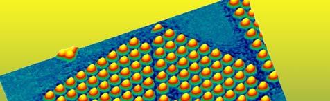
5 C 60 /Ag(111) 40nm 400 nm x 400 nm image of clean Ag film 200 nm x 200 nm image of partial coverage of C60/Ag/mica at room temperature High resolution image: C60 chain decorating a step -- C. Tao et al, PRB, 73, (2006)


6 C 60 and Step Motion Silver atomic motion at step edge is fast - time constant of a microsecond Individual C 60 at step edge may be stationary for 100s of seconds Strong charge transfer in C 60 binding If C60 and Ag motion are correlated, C60 will act as pinning site for Ag step fluctuations -- C. Tao et al, PRB, 73, (2006)
7 C 60 /Ag(111) y [112] x L 40nm Choose different C60 separations and measure the effect on the Ag step edge variations x(t) in between the C60s. G(t) = Clean Ag steps (no C60): n=4 ( x(t) x(0) ) 2 = ( ) 2Γ 1 1/n π kt β n 1 n t a n +1 τ Interesting measurement time effects: A. Bondarchuk et al, PRB /n

8 Fluctuation Modes Steps fluctuate like strings - with all wavelengths allowed by the boundary and/or observation conditions. The fluctuation correlations we observe are the combination of all the available wavelengths. 2π / a G(t) = G q () t dq q = 2π /λ q min The overall width of the fluctuations is determined by the the system size L ~ λ max : ( ) 2 = ktl -- Jeong&Williams, SSR w 2 eq = x(t) x 12 β L

9 Effective system sizes 250 Effective System Size (nm) Two step orientations Different β values Step length (nm) No significant dependence on C60 separation for either! Effective system sizes are the same as for steps on clean Ag L -- C. Tao et al, PRB, 73, (2006)


10 Circular Ag islands decorated by C 60 rings 100nm 30nm 30nm By carefully increasing the C 60 coverage, we create circular C60 structures -- C. Tao et al, Nano Letters (2007)


 -- T.")
11 C 60 Motion with chain Local motion of C 60 molecules is evident. Bimodal hops correlate with a C60 kink displacement between two favorable underlying Ag sites. -- C. Tao et al, Nano Letters (2007) -- T. Stasevich et al., in prep (2007)
 Digitized C 60 rings Time per image = 52.")
12 Shape fluctuations STM image of a Ag island surrounded by a C 60 ring (line time 0.1 s, 512 lines) Digitized C 60 rings Time per image = 52.4 s Averaged C 60 ring shape Total time = 3458 s
13 Fluctuation Modes of a Ring Analogy to fluctuations of an island bounded by a step Define modes of fluctuation r k (t) = π π r θ,t ( ) exp( ikθ)dθ k I


14 Same movie again Digitized C 60 rings Time per image = 52.4 s, Total time = 3458 s
15 Analysis of Island Fluctuations* Measure radial displacements: g θ,t ( )= R θ,t ( ) R <R> R(θ) θ Angular Fourier transform: g k = 1 2N N n= N 1 ( ) gnπ /N exp(knπ /N) Modal time-correlation function: g k (t + t 0 ) g k (t o ) 2 = ktr 2π β k 2 ( 1 e 2t /τ k ) *Khare & Einstein PRB 54,
16 Modal Time Correlation Functions G k (t), nm 2 k=2 k=5 Fitting individual curves yields A k and τ k g k (t + t 0 ) g k (t o ) 2 = G k ()= t A ( k 1 e 2t /τ ) k -- C. Tao et al, Nano Letters (2007) A k = ktr 2π β k 2 τ k = kt Γ z β R k z = 4, conserved noise z = 2, non-conserved noise z
17 C 60 Ring Modes C60, R = 12.4 nm Mode 4: (A 4 ) 1/2 = 0.08 nm 4 = 120 s Mode 12: (A 12 ) 1/2 = 0.03 nm 12 = 12 s A k = (0.009nm)(R/ k α ), with α = 1.88 k = (11.5nm -2 s)(r/k) z, with z = 1.85 z = 2! Non-conserved Noise - not the same as clean Ag (z = 4) -- C. Tao et al, Nano Letters (2007)
18 C 60 and Ag island edge C60, R = 12.4 nm Mode 4: (A 4 ) 1/2 = 0.08 nm 4 = 120 s Mode 12: (A 12 ) 1/2 = 0.03 nm 12 = 12 s Clean Ag, R = 12.4 nm Mode 4: (A 4 ) 1/2 = nm 4 = 0.8 s Mode 12: (A 12 ) 1/2 = nm 12 = s -- C. Tao et al, PRB, 73, (2006) _ A. Bondarchuk et al, PRB
 Mode fluctuations will be much slower, and large enough in amplitude (0.")
19 Impact of Structure Fluctuations Metal-molecule interface Transmission probability across a molecular bridge similar to tunneling - exponential dependence on width of gap + strong dependence on specific metal configuration at contact point Motion of individual metal atoms can be fast - >10 6 Hz (example Ag) Mode fluctuations will be much slower, and large enough in amplitude (0.01 nm) to significantly affect transmission probability Conserved and non-conserved noise modes will contribute distinct frequency characteristics: A k ( f k =1/τ k )= 0.10nm3 1/2 f k silver (conserved) C60 (non-conserved) A k R ( f k =1/τ k )= 8x10 4 nm 3 R f k 1

20 Line Boundaries and Electrical Transport Fluctuating surface steps affect and are affected by internal scattering of charge carriers from surface/interface nm Ag nanowire Synthesis - Murphy group USC STM - Williams group UMD The effects of interfaces with fluctuations in structure are important when the surface/volume ratio is large or when interfaces are the primarily source of carrier scattering or trapping
21 Electron-scattering Force Z w = -19 for Ag Z w =-20e Z w =-43e Z w =-17e Z w =-16e Z w =-2e Z w =-6e P.J. Rous, Electromigration force at stepped Al Surfaces, Physical Review B59, 7719, Force on diffusing atom: F=ez*E; E = electric field Wind force: z*=n o Lσ tr n o = electron density, ~ 0.1 Å -3 (58.5 nm -3 for Ag) L = mean free path, ~ 100 Å (~60 nm for Ag) σ tr = transport cross section at E f ; ~ 1 Å 2 (~ha~0.07nm 2 for a step edge) P.J. Rous et al., Surface Sci. 315, L995, 1994; P.J. Rous, Phys. Rev. B61,
22 Weak Force For metals (e.g. Ag), resistivity is low Fa ~10-7 ev/unit cell Linear perturbation of Langevin equation for step motion t Γ 4β k B T 4 x 4 Γ 4 F 2 k B Ta a x 2 a y( x,t)= η x,t ( ) Measure Effects on step fluctuations, x(t). For Ag, the step fluctuations occur via atomic diffusion along the step edge Expect modified fluctuation correlations: P.Rous et al., in preparation for NJP (2007)
23 Correlation function with EM - Theory G eq ( ) 2Γ 3/4 ()= t π τ EM = kt β ( Fa) τ 2 h G EM t () G eq ()1± t kt β t τ EM 3/4 ( Γ h t) 1/4 1/2 1 Force downhill Force uphill Wind force causes deviations in time correlation of step wandering P.Rous et al., in preparation for NJP (2007) Downhill Force

24 Ag Thin Film with Bias Current Current biasing to >10 5 A/cm 2 Fit value is τ EM = 50s τ η = 1.7x10⁻⁸ s A. Bondarchuk et al., submitted
25 Comparison with Control Evaluation of relative chi-squared for fit as a function of the fit parameter τ em. Biased sample (j = 4x10 5 A/cm 2 ) T = 380K Unbiased sample (j = 0) T = 325K 35s 80s electromigration time const., τ em 10 2 s s electromigration time const., τ em
26 F w 2 = kt β τ h aτ em F w = z * ee = z * eρj Analysis Calculate step stiffness using kink energy ev* ρ =1.8x10 6 Ω cm T = 325K ρ = 2.2x10 6 Ω cm T = 370K F = -2.7x10⁻⁵ ev/nm for J nom = 4x10 5 A/cm 2 F = -9.6x10⁻⁶ ev/nm for J nom = 1x10 5 A/cm 2 100e < z * < 300e Forces and effective valence substantially larger than calculated value for isolated Ag adatom on a Ag terrace (z* = -19) Akustsu&Akustsu J. Phys. Cond. C *T. Stasevich et al., PRB (2005) 2 β a kta = 2 3 exp ε kt

27 Electron scattering at steps/kinks F w F tan *P.J. Rous et al., PRB, 7719, 1999 T.S. Rahman, SS M. Giesen SS Geometric blocking of current flow at steps increases scattering ~x2* Kink sites may enhance geometric blocking Only tangential component of force affects step-edge motion Kink sites have enhanced charge density Kink sites modify activation barrier for stepedge diffusion
28 Surface Resistivity Conservation of momentum requires opposing effect on charge carriers, modifying transport characteristics: l f = film thickness ρ l s f F w n k eηj = ( 3 ±1.5nm3 )ρ o n k = kink density For 20 nm scale structures with 1 nm step spacing, Δρ s ~ 0.3ρ Structural fluctuations will affect surface resistivity, creating frequency signature in transport

 Device fabrication: Lithographic fabrication of electrodes onto")
29 Atomically thin-sheet: Graphene Novel electronic properties: understanding of fundamental mechanisms in flux trapped charges and morphology both important Preparation: Mechanical exfoliation onto SiO2 (Geim, Kim) Surface segregation on SiC (de Heer) Device fabrication: Lithographic fabrication of electrodes onto graphene


30 Experimental Issues How to find the device - Why the device need to be found - Conducting substrate usually needed - Combing SEM, AFM and STM, we can land tip on 1 nm 2 area M. Ishigami, J.H. Chen, W.G. Cullen, E.D. Williams, and M.S. Fuhrer, Nanoletters, submitted (2007


31 Experimental Issues How to clean graphene - PMMA residue remains on carbon part of the device after lift-off - Commercial resist remover doesn t work - Special cleaning procedure* can remove PMMA residue - STM image show atomically clean graphene device 300 nm 500 nm Cleaning Non-contact AFM image 300 nm in UHV M. Ishigami, J.H. Chen, W.G. Cullen, E.D. Williams, and M.S. Fuhrer, Nanoletters, submitted (2007

![0 V and I tunnel = 24 pa] Processing residues are completely removed Large](/docs-images/90/104338135/images/32-1.jpg "corrugation Hexagonal and triangular patterns apparent M. Ishigami, J.H. Chen, W.G.")
32 STM images of a graphene device 2 nm 5 Å 2.5 Ǻ [V sample = 1.1 V and I tunnel = 0.3 na] [V sample = 1.0 V and I tunnel = 24 pa] Processing residues are completely removed Large corrugation Hexagonal and triangular patterns apparent M. Ishigami, J.H. Chen, W.G. Cullen, E.D. Williams, and M.S. Fuhrer, Nanoletters, submitted (2007
33 Two Dimensional Morphology of Graphene Non-contact AFM image in UHV 0.05 Silicon Graphene Probability 200 nm Oxide-graphene boundary Height [nm] σ oxide = 3.1 Å and σ graphene = 1.9 Å Graphene 60% smoother than SiO 2 M. Ishigami, J.H. Chen, W.G. Cullen, E.D. Williams, and M.S. Fuhrer, Nanoletters, submitted (2007
34 Non-contact AFM image in UHV Origin of Graphene Roughness 0.1 ξ 2 G = 2σ G ~ b x G(x) [nm 2 ] 0.01 Graphene Silicon Oxide Oxide-graphene boundary 200 nm 10 Distance [nm] G( x) = ( z( x + x) z( x 2 0 0)) Morphology defined by the substrate b oxide =1.2, b graphene =1.1 Finite graphene stiffness ξ oxide =23 nm, ξ graphene =32 nm M. Ishigami, J.H. Chen, W.G. Cullen, E.D. Williams, and M.S. Fuhrer, Nanoletters, submitted (2007
35 Graphene Corrugation Physical origins of corrugation: Model 1: Intrinsic graphene property constrained via interaction with interface Model 2: Corrugations determined by relatively strong interaction with SiO2 M. Ishigami, J.H. Chen, W.G. Cullen, E.D. Williams, and M.S. Fuhrer, Nanoletters, submitted (2007)
36 Model 1: Intrinsic morphology H. Aranda-Espinoza and D. Lavallee Structure factor of flexible membranes Europhys. Lett, 43 pp (1998) F = 1 2 κ [ 2 h(x, y) ] Vh 2 ( x,y) κ = bending modulus (rigidity) Et 3 κ = 12 1 ν 2 =1.1x10 19 J ( ) Graphene V = quadratic constraining potential ξ ( κ /V) 1/4 h(x,y) 2 = kt 8 κv ( ) 1/2 ( h(r) h(0) ) 2 ~ r 2 r 2 dependence equivalent to 2H = 2. Experimentally 2H ~1 graphene Substrate V Van der Waals type interaction - expand potential V(h) to 2d order around h o h h o
37 Model 2: Substrate-determined morphology Estimated relative energies appear reasonable: Hamaker coefficients: SiO 2 : 650 x10-21 J graphite: 223 x10-21 J h o =4.2Å Adhesion energy ~ 14meV/Å 2 E bend = Et 3 ( ) 24 1 ν 2 What is the minimum curvature R for which adhesion overcomes bending energy? R > 5.5Å About the radius of a single walled CNT 1 R 2 graphene h o Substrate Van der Waals type interaction - constrains graphene to substrate shape except for areas of very sharp curvature
38 Interface Fluctuations Key Observations Collective motion (structural modes) of nanometer structures (~70 C 60 ) observed in 1Hz range with amplitude on the order of 0.1 nm - sufficient to perturb transmission probabilities at electrode interfaces Different mechanisms of mode fluctuation yield different frequency signatures (f -1 and f -1/2 ) Surface Resistivity Charge carrier scattering off of Ag steps sufficient to bias equilibrium fluctations on time scale of 5 s Surface resistivity due to fluctuating kink structure can be ~10% of bulk resistivity for 10nm nanostructure Ultra-thin sheet subject to mechanical constraints (graphene) represents interesting possibilities for coordinating morphology with electrical properties


39 Experimental Statistical Mechanics at the Nanoscale Nanoscale structures: fabrication, stability and evolution Survival! First passage to annihilation
SUPPLEMENTARY NOTES Supplementary Note 1: Fabrication of Scanning Thermal Microscopy Probes
 SUPPLEMENTARY NOTES Supplementary Note 1: Fabrication of Scanning Thermal Microscopy Probes Fabrication of the scanning thermal microscopy (SThM) probes is summarized in Supplementary Fig. 1 and proceeds
Optimizing Graphene Morphology on SiC(0001)
") Optimizing Graphene Morphology on SiC(0001) James B. Hannon Rudolf M. Tromp Graphene sheets Graphene sheets can be formed into 0D,1D, 2D, and 3D structures Chemically inert Intrinsically high carrier mobility
Optimizing Graphene Morphology on SiC(0001) James B. Hannon Rudolf M. Tromp Graphene sheets Graphene sheets can be formed into 0D,1D, 2D, and 3D structures Chemically inert Intrinsically high carrier mobility
Supplementary information for Tunneling Spectroscopy of Graphene-Boron Nitride Heterostructures
 Supplementary information for Tunneling Spectroscopy of Graphene-Boron Nitride Heterostructures F. Amet, 1 J. R. Williams, 2 A. G. F. Garcia, 2 M. Yankowitz, 2 K.Watanabe, 3 T.Taniguchi, 3 and D. Goldhaber-Gordon
Impact of Calcium on Transport Property of Graphene. Jyoti Katoch and Masa Ishigami*
 Impact of Calcium on Transport Property of Graphene Jyoti Katoch and Masa Ishigami* Department of Physics and Nanoscience Technology Center, University of Central Florida, Orlando, FL, 32816 *Corresponding
Carbon based Nanoscale Electronics
 Carbon based Nanoscale Electronics 09 02 200802 2008 ME class Outline driving force for the carbon nanomaterial electronic properties of fullerene exploration of electronic carbon nanotube gold rush of
Fabrication and Measurement of Spin Devices. Purdue Birck Presentation
 Fabrication and Measurement of Spin Devices Zhihong Chen School of Electrical and Computer Engineering Birck Nanotechnology Center, Discovery Park Purdue University Purdue Birck Presentation zhchen@purdue.edu
Graphene photodetectors with ultra-broadband and high responsivity at room temperature
 SUPPLEMENTARY INFORMATION DOI: 10.1038/NNANO.2014.31 Graphene photodetectors with ultra-broadband and high responsivity at room temperature Chang-Hua Liu 1, You-Chia Chang 2, Ted Norris 1.2* and Zhaohui
SUPPLEMENTARY INFORMATION
 SUPPLEMENTARY INFORMATION Transforming Fullerene into Graphene Quantum Dots Jiong Lu, Pei Shan Emmeline Yeo, Chee Kwan Gan, Ping Wu and Kian Ping Loh email: chmlohkp@nus.edu.sg Contents Figure S1 Transformation
There's Plenty of Room at the Bottom
 There's Plenty of Room at the Bottom 12/29/1959 Feynman asked why not put the entire Encyclopedia Britannica (24 volumes) on a pin head (requires atomic scale recording). He proposed to use electron microscope
Overview. Carbon in all its forms. Background & Discovery Fabrication. Important properties. Summary & References. Overview of current research
 Graphene Prepared for Solid State Physics II Pr Dagotto Spring 2009 Laurene Tetard 03/23/09 Overview Carbon in all its forms Background & Discovery Fabrication Important properties Overview of current
(a) (b) Supplementary Figure 1. (a) (b) (a) Supplementary Figure 2. (a) (b) (c) (d) (e)
 (b) Supplementary Figure 1. (a) (b) (a) Supplementary Figure 2. (a) (b) (c) (d) (e)") (a) (b) Supplementary Figure 1. (a) An AFM image of the device after the formation of the contact electrodes and the top gate dielectric Al 2 O 3. (b) A line scan performed along the white dashed line
(a) (b) Supplementary Figure 1. (a) An AFM image of the device after the formation of the contact electrodes and the top gate dielectric Al 2 O 3. (b) A line scan performed along the white dashed line
Olivier Bourgeois Institut Néel
 Olivier Bourgeois Institut Néel Outline Introduction: necessary concepts: phonons in low dimension, characteristic length Part 1: Transport and heat storage via phonons Specific heat and kinetic equation
Surface atoms/molecules of a material act as an interface to its surrounding environment;
 1 Chapter 1 Thesis Overview Surface atoms/molecules of a material act as an interface to its surrounding environment; their properties are often complicated by external adsorbates/species on the surface
Wafer-scale fabrication of graphene
 Wafer-scale fabrication of graphene Sten Vollebregt, MSc Delft University of Technology, Delft Institute of Mircosystems and Nanotechnology Delft University of Technology Challenge the future Delft University
Surface Physics Surface Diffusion. Assistant: Dr. Enrico Gnecco NCCR Nanoscale Science
 Surface Physics 008 8. Surface Diffusion Assistant: Dr. Enrico Gnecco NCCR Nanoscale Science Random-Walk Motion Thermal motion of an adatom on an ideal crystal surface: - Thermal excitation the adatom
Scanning Tunneling Microscopy
 Scanning Tunneling Microscopy Scanning Direction References: Classical Tunneling Quantum Mechanics Tunneling current Tunneling current I t I t (V/d)exp(-Aφ 1/2 d) A = 1.025 (ev) -1/2 Å -1 I t = 10 pa~10na
ICTP Conference Graphene Week 2008
 1960-3 ICTP Conference Graphene Week 2008 25-29 August 2008 Current-induced cleaning of graphene J. Moser CIN2 Barcelona, Campus UAB, Bellaterra, Spain A. Barreiro CIN2 Barcelona, Campus UAB, Bellaterra,
Transport through Andreev Bound States in a Superconductor-Quantum Dot-Graphene System
 Transport through Andreev Bound States in a Superconductor-Quantum Dot-Graphene System Nadya Mason Travis Dirk, Yung-Fu Chen, Cesar Chialvo Taylor Hughes, Siddhartha Lal, Bruno Uchoa Paul Goldbart University
Supplementary Figure 1 Experimental setup for crystal growth. Schematic drawing of the experimental setup for C 8 -BTBT crystal growth.
 Supplementary Figure 1 Experimental setup for crystal growth. Schematic drawing of the experimental setup for C 8 -BTBT crystal growth. Supplementary Figure 2 AFM study of the C 8 -BTBT crystal growth
Adhesion of membranes and filaments on patterned surfaces
 Adhesion of membranes and filaments on patterned surfaces Olivier Pierre-Louis CNRS / Oxford Theoretical Physics 1 Keble Road, Oxford OX1 3NP, UK olivier.pierre-louis@physics.ox.ac.uk Spring 2008 Nanotube
Electric Field-Dependent Charge-Carrier Velocity in Semiconducting Carbon. Nanotubes. Yung-Fu Chen and M. S. Fuhrer
 Electric Field-Dependent Charge-Carrier Velocity in Semiconducting Carbon Nanotubes Yung-Fu Chen and M. S. Fuhrer Department of Physics and Center for Superconductivity Research, University of Maryland,
Initial Stages of Growth of Organic Semiconductors on Graphene
 Initial Stages of Growth of Organic Semiconductors on Graphene Presented by: Manisha Chhikara Supervisor: Prof. Dr. Gvido Bratina University of Nova Gorica Outline Introduction to Graphene Fabrication
Lecture 6: 2D FET Electrostatics
 Lecture 6: 2D FET Electrostatics 2016-02-01 Lecture 6, High Speed Devices 2014 1 Lecture 6: III-V FET DC I - MESFETs Reading Guide: Liu: 323-337 (he mainly focuses on the single heterostructure FET) Jena:
Electronic transport in low dimensional systems
 Electronic transport in low dimensional systems For example: 2D system l
Appendix 1: List of symbols
 Appendix 1: List of symbols Symbol Description MKS Units a Acceleration m/s 2 a 0 Bohr radius m A Area m 2 A* Richardson constant m/s A C Collector area m 2 A E Emitter area m 2 b Bimolecular recombination
C. Show your answer in part B agrees with your answer in part A in the limit that the constant c 0.
 Problem #1 A. A projectile of mass m is shot vertically in the gravitational field. Its initial velocity is v o. Assuming there is no air resistance, how high does m go? B. Now assume the projectile is
Quantum Confinement in Graphene
 Quantum Confinement in Graphene from quasi-localization to chaotic billards MMM dominikus kölbl 13.10.08 1 / 27 Outline some facts about graphene quasibound states in graphene numerical calculation of
PERSISTENCE AND SURVIVAL IN EQUILIBRIUM STEP FLUCTUATIONS. Chandan Dasgupta
 PERSISTENCE AND SURVIVAL IN EQUILIBRIUM STEP FLUCTUATIONS Chandan Dasgupta Centre for Condensed Matter Theory Department of Physics Indian Institute of Science, Bangalore http://www.physics.iisc.ernet.in/~cdgupta
Recap (so far) Low-Dimensional & Boundary Effects
 Low-Dimensional & Boundary Effects") Recap (so far) Ohm s & Fourier s Laws Mobility & Thermal Conductivity Heat Capacity Wiedemann-Franz Relationship Size Effects and Breakdown of Classical Laws 1 Low-Dimensional & Boundary Effects Energy
Recap (so far) Ohm s & Fourier s Laws Mobility & Thermal Conductivity Heat Capacity Wiedemann-Franz Relationship Size Effects and Breakdown of Classical Laws 1 Low-Dimensional & Boundary Effects Energy
STM and graphene. W. W. Larry Pai ( 白偉武 ) Center for condensed matter sciences, National Taiwan University NTHU, 2013/05/23
 Center for condensed matter sciences, National Taiwan University NTHU, 2013/05/23") STM and graphene W. W. Larry Pai ( 白偉武 ) Center for condensed matter sciences, National Taiwan University NTHU, 2013/05/23 Why graphene is important: It is a new form of material (two dimensional, single
STM and graphene W. W. Larry Pai ( 白偉武 ) Center for condensed matter sciences, National Taiwan University NTHU, 2013/05/23 Why graphene is important: It is a new form of material (two dimensional, single
Intrinsic Response of Graphene Vapor Sensors
 Intrinsic Response of Graphene Vapor Sensors Yaping Dan, Ye Lu, Nicholas J. Kybert, A. T. Charlie Johnson Department of Electrical and Systems Engineering, University of Pennsylvania, Philadelphia, PA
STM: Scanning Tunneling Microscope
 STM: Scanning Tunneling Microscope Basic idea STM working principle Schematic representation of the sample-tip tunnel barrier Assume tip and sample described by two infinite plate electrodes Φ t +Φ s =
I-V characteristics model for Carbon Nanotube Field Effect Transistors
 International Journal of Engineering & Technology IJET-IJENS Vol:14 No:04 33 I-V characteristics model for Carbon Nanotube Field Effect Transistors Rebiha Marki, Chérifa Azizi and Mourad Zaabat. Abstract--
CH676 Physical Chemistry: Principles and Applications. CH676 Physical Chemistry: Principles and Applications
 CH676 Physical Chemistry: Principles and Applications History of Nanotechnology: Time Line Democritus in ancient Greece: concept of atom 1900 : Rutherford : discovery of atomic nucleus The first TEM was
Supporting data for On the structure and topography of free-standing chemically modified graphene
 1 Supporting data for On the structure and topography of free-standing chemically modified graphene N R Wilson 1, P A Pandey 1, R Beanland 1, J P Rourke 2, U Lupo 1, G Rowlands 1 and R A Römer 1,3 1 Department
SUPPLEMENTARY INFORMATION
 SUPPLEMENTARY INFORMATION Controlled Ripple Texturing of Suspended Graphene and Ultrathin Graphite Membranes Wenzhong Bao, Feng Miao, Zhen Chen, Hang Zhang, Wanyoung Jang, Chris Dames, Chun Ning Lau *
2. TranSIESTA 1. SIESTA. DFT In a Nutshell. Introduction to SIESTA. Boundary Conditions: Open systems. Greens functions and charge density
 1. SIESTA DFT In a Nutshell Introduction to SIESTA Atomic Orbitals Capabilities Resources 2. TranSIESTA Transport in the Nanoscale - motivation Boundary Conditions: Open systems Greens functions and charge
& Dirac Fermion confinement Zahra Khatibi
 Graphene & Dirac Fermion confinement Zahra Khatibi 1 Outline: What is so special about Graphene? applications What is Graphene? Structure Transport properties Dirac fermions confinement Necessity External
single-electron electron tunneling (SET)
") single-electron electron tunneling (SET) classical dots (SET islands): level spacing is NOT important; only the charging energy (=classical effect, many electrons on the island) quantum dots: : level spacing
single-electron electron tunneling (SET) classical dots (SET islands): level spacing is NOT important; only the charging energy (=classical effect, many electrons on the island) quantum dots: : level spacing
Novel materials and nanostructures for advanced optoelectronics
 Novel materials and nanostructures for advanced optoelectronics Q. Zhuang, P. Carrington, M. Hayne, A Krier Physics Department, Lancaster University, UK u Brief introduction to Outline Lancaster University
SUPPLEMENTARY INFORMATION
 SUPPLEMENTARY INFORMATION Facile Synthesis of High Quality Graphene Nanoribbons Liying Jiao, Xinran Wang, Georgi Diankov, Hailiang Wang & Hongjie Dai* Supplementary Information 1. Photograph of graphene
Quasi-periodic nanostructures grown by oblique angle deposition
 JOURNAL OF APPLIED PHYSICS VOLUME 94, NUMBER 12 15 DECEMBER 2003 Quasi-periodic nanostructures grown by oblique angle deposition T. Karabacak, a) G.-C. Wang, and T.-M. Lu Department of Physics, Applied
Graphite, graphene and relativistic electrons
 Graphite, graphene and relativistic electrons Introduction Physics of E. graphene Y. Andrei Experiments Rutgers University Transport electric field effect Quantum Hall Effect chiral fermions STM Dirac
Three-terminal quantum-dot thermoelectrics
 Three-terminal quantum-dot thermoelectrics Björn Sothmann Université de Genève Collaborators: R. Sánchez, A. N. Jordan, M. Büttiker 5.11.2013 Outline Introduction Quantum dots and Coulomb blockade Quantum
Sampling Time Effects for Persistence and Survival in Step Structural Fluctuations
 1 Sampling Time Effects for Persistence and Survival in Step Structural Fluctuations D.B. Dougherty 1, C. Tao 1, O. Bondarchuk 18, W.G. Cullen 1, and E.D. Williams 1,2 Department of Physics 1 and Institute
A BIT OF MATERIALS SCIENCE THEN PHYSICS
 GRAPHENE AND OTHER D ATOMIC CRYSTALS Andre Geim with many thanks to K. Novoselov, S. Morozov, D. Jiang, F. Schedin, I. Grigorieva, J. Meyer, M. Katsnelson A BIT OF MATERIALS SCIENCE THEN PHYSICS CARBON
Carbon nanotubes: nanomechanics, manipulation, and electronic devices
 Ž. Applied Surface Science 141 1999 201 209 Carbon nanotubes: nanomechanics, manipulation, and electronic devices Ph. Avouris ), T. Hertel, R. Martel, T. Schmidt, H.R. Shea, R.E. Walkup IBM Research DiÕision,
Graphene. Tianyu Ye November 30th, 2011
 Graphene Tianyu Ye November 30th, 2011 Outline What is graphene? How to make graphene? (Exfoliation, Epitaxial, CVD) Is it graphene? (Identification methods) Transport properties; Other properties; Applications;
Supplementary Information
 Electronic Supplementary Material (ESI) for Nanoscale. This journal is The Royal Society of Chemistry 2016 Electronic Supplementary Material (ESI) for Nanoscale. This journal is The Royal Society of Chemistry
Lecture 4 Scanning Probe Microscopy (SPM)
") Lecture 4 Scanning Probe Microscopy (SPM) General components of SPM; Tip --- the probe; Cantilever --- the indicator of the tip; Tip-sample interaction --- the feedback system; Scanner --- piezoelectric
Lecture 4 Scanning Probe Microscopy (SPM) General components of SPM; Tip --- the probe; Cantilever --- the indicator of the tip; Tip-sample interaction --- the feedback system; Scanner --- piezoelectric
Dynamics of step fluctuations on a chemically heterogeneous surface of AlÕSi )Ã)
Ã)") Dynamics of step fluctuations on a chemically heterogeneous surface of AlÕSi 111 - )Ã) I. Lyubinetsky, D. B. Dougherty, T. L. Einstein, and E. D. Williams* University of Maryland, Department of Physics
Dynamics of step fluctuations on a chemically heterogeneous surface of AlÕSi 111 - )Ã) I. Lyubinetsky, D. B. Dougherty, T. L. Einstein, and E. D. Williams* University of Maryland, Department of Physics
Lectures Graphene and
 Lectures 15-16 Graphene and carbon nanotubes Graphene is atomically thin crystal of carbon which is stronger than steel but flexible, is transparent for light, and conducts electricity (gapless semiconductor).
STM spectroscopy (STS)
") STM spectroscopy (STS) di dv 4 e ( E ev, r) ( E ) M S F T F Basic concepts of STS. With the feedback circuit open the variation of the tunneling current due to the application of a small oscillating voltage
STM spectroscopy (STS) di dv 4 e ( E ev, r) ( E ) M S F T F Basic concepts of STS. With the feedback circuit open the variation of the tunneling current due to the application of a small oscillating voltage
Spatially resolving density-dependent screening around a single charged atom in graphene
 Supplementary Information for Spatially resolving density-dependent screening around a single charged atom in graphene Dillon Wong, Fabiano Corsetti, Yang Wang, Victor W. Brar, Hsin-Zon Tsai, Qiong Wu,
b imaging by a double tip potential
 Supplementary Figure Measurement of the sheet conductance. Resistance as a function of probe spacing including D and 3D fits. The distance is plotted on a logarithmic scale. The inset shows corresponding
NiCl2 Solution concentration. Etching Duration. Aspect ratio. Experiment Atmosphere Temperature. Length(µm) Width (nm) Ar:H2=9:1, 150Pa
 Width (nm) Ar:H2=9:1, 150Pa") Experiment Atmosphere Temperature #1 # 2 # 3 # 4 # 5 # 6 # 7 # 8 # 9 # 10 Ar:H2=9:1, 150Pa Ar:H2=9:1, 150Pa Ar:H2=9:1, 150Pa Ar:H2=9:1, 150Pa Ar:H2=9:1, 150Pa Ar:H2=9:1, 150Pa Ar:H2=9:1, 150Pa Ar:H2=9:1,
Experiment Atmosphere Temperature #1 # 2 # 3 # 4 # 5 # 6 # 7 # 8 # 9 # 10 Ar:H2=9:1, 150Pa Ar:H2=9:1, 150Pa Ar:H2=9:1, 150Pa Ar:H2=9:1, 150Pa Ar:H2=9:1, 150Pa Ar:H2=9:1, 150Pa Ar:H2=9:1, 150Pa Ar:H2=9:1,
Supporting information
 Supporting information Influence of electrolyte composition on liquid-gated carbon-nanotube and graphene transistors By: Iddo Heller, Sohail Chatoor, Jaan Männik, Marcel A. G. Zevenbergen, Cees Dekker,
III-V nanostructured materials synthesized by MBE droplet epitaxy
 III-V nanostructured materials synthesized by MBE droplet epitaxy E.A. Anyebe 1, C. C. Yu 1, Q. Zhuang 1,*, B. Robinson 1, O Kolosov 1, V. Fal ko 1, R. Young 1, M Hayne 1, A. Sanchez 2, D. Hynes 2, and
Supplementary Materials for
 advances.sciencemag.org/cgi/content/full/3/10/e1701661/dc1 Supplementary Materials for Defect passivation of transition metal dichalcogenides via a charge transfer van der Waals interface Jun Hong Park,
Branislav K. Nikolić
 First-principles quantum transport modeling of thermoelectricity in nanowires and single-molecule nanojunctions Branislav K. Nikolić Department of Physics and Astronomy, University of Delaware, Newark,
Hydrogenated Graphene
 Hydrogenated Graphene Stefan Heun NEST, Istituto Nanoscienze-CNR and Scuola Normale Superiore Pisa, Italy Outline Epitaxial Graphene Hydrogen Chemisorbed on Graphene Hydrogen-Intercalated Graphene Outline
1. Nanotechnology & nanomaterials -- Functional nanomaterials enabled by nanotechnologies.
 Novel Nano-Engineered Semiconductors for Possible Photon Sources and Detectors NAI-CHANG YEH Department of Physics, California Institute of Technology 1. Nanotechnology & nanomaterials -- Functional nanomaterials
Carbon Nanotube Thin-Films & Nanoparticle Assembly
 Nanodevices using Nanomaterials : Carbon Nanotube Thin-Films & Nanoparticle Assembly Seung-Beck Lee Division of Electronics and Computer Engineering & Department of Nanotechnology, Hanyang University,
Multiscale Modeling of Epitaxial Growth Processes: Level Sets and Atomistic Models
 Multiscale Modeling of Epitaxial Growth Processes: Level Sets and Atomistic Models Russel Caflisch 1, Mark Gyure 2, Bo Li 4, Stan Osher 1, Christian Ratsch 1,2, David Shao 1 and Dimitri Vvedensky 3 1 UCLA,
Carbon Nanotubes in Interconnect Applications
 Carbon Nanotubes in Interconnect Applications Page 1 What are Carbon Nanotubes? What are they good for? Why are we interested in them? - Interconnects of the future? Comparison of electrical properties
Thermal Transport in Graphene and other Two-Dimensional Systems. Li Shi. Department of Mechanical Engineering & Texas Materials Institute
 Thermal Transport in Graphene and other Two-Dimensional Systems Li Shi Department of Mechanical Engineering & Texas Materials Institute Outline Thermal Transport Theories and Simulations of Graphene Raman
2) Atom manipulation. Xe / Ni(110) Model: Experiment:
 Atom manipulation. Xe / Ni(110) Model: Experiment:") 2) Atom manipulation D. Eigler & E. Schweizer, Nature 344, 524 (1990) Xe / Ni(110) Model: Experiment: G.Meyer, et al. Applied Physics A 68, 125 (1999) First the tip is approached close to the adsorbate
2) Atom manipulation D. Eigler & E. Schweizer, Nature 344, 524 (1990) Xe / Ni(110) Model: Experiment: G.Meyer, et al. Applied Physics A 68, 125 (1999) First the tip is approached close to the adsorbate
From nanophysics research labs to cell phones. Dr. András Halbritter Department of Physics associate professor
 From nanophysics research labs to cell phones Dr. András Halbritter Department of Physics associate professor Curriculum Vitae Birth: 1976. High-school graduation: 1994. Master degree: 1999. PhD: 2003.
Electrical Contacts to Carbon Nanotubes Down to 1nm in Diameter
 1 Electrical Contacts to Carbon Nanotubes Down to 1nm in Diameter Woong Kim, Ali Javey, Ryan Tu, Jien Cao, Qian Wang, and Hongjie Dai* Department of Chemistry and Laboratory for Advanced Materials, Stanford
Low Bias Transport in Graphene: An Introduction
 Lecture Notes on Low Bias Transport in Graphene: An Introduction Dionisis Berdebes, Tony Low, and Mark Lundstrom Network for Computational Nanotechnology Birck Nanotechnology Center Purdue University West
Transparent Electrode Applications
 Transparent Electrode Applications LCD Solar Cells Touch Screen Indium Tin Oxide (ITO) Zinc Oxide (ZnO) - High conductivity - High transparency - Resistant to environmental effects - Rare material (Indium)
Electronic structure and transport in silicon nanostructures with non-ideal bonding environments
 Purdue University Purdue e-pubs Other Nanotechnology Publications Birck Nanotechnology Center 9-15-2008 Electronic structure and transport in silicon nanostructures with non-ideal bonding environments
Instrumentation and Operation
 Instrumentation and Operation 1 STM Instrumentation COMPONENTS sharp metal tip scanning system and control electronics feedback electronics (keeps tunneling current constant) image processing system data
SUPPLEMENTARY INFORMATION
 SUPPLEMENTARY INFORMATION Flexible, high-performance carbon nanotube integrated circuits Dong-ming Sun, Marina Y. Timmermans, Ying Tian, Albert G. Nasibulin, Esko I. Kauppinen, Shigeru Kishimoto, Takashi
Electrostatics of Nanowire Transistors
 Electrostatics of Nanowire Transistors Jing Guo, Jing Wang, Eric Polizzi, Supriyo Datta and Mark Lundstrom School of Electrical and Computer Engineering Purdue University, West Lafayette, IN, 47907 ABSTRACTS
collisions of electrons. In semiconductor, in certain temperature ranges the conductivity increases rapidly by increasing temperature
 1.9. Temperature Dependence of Semiconductor Conductivity Such dependence is one most important in semiconductor. In metals, Conductivity decreases by increasing temperature due to greater frequency of
Lecture 11 - Phonons II - Thermal Prop. Continued
 Phonons II - hermal Properties - Continued (Kittel Ch. 5) Low High Outline Anharmonicity Crucial for hermal expansion other changes with pressure temperature Gruneisen Constant hermal Heat ransport Phonon
Elementary Process of Electromigration at Metallic Nanojunctions in the Ballistic Regime
 Elementary Process of Electromigration at Metallic Nanojunctions in the Ballistic Regime Kaz Hirakawa Institute of Industrial Science, University of Tokyo CREST, JST collaborators: Akinori Umeno, Kenji
Graphene: Plane and Simple Electrical Metrology?
 Graphene: Plane and Simple Electrical Metrology? R. E. Elmquist, F. L. Hernandez-Marquez, M. Real, T. Shen, D. B. Newell, C. J. Jacob, and G. R. Jones, Jr. National Institute of Standards and Technology,
Application of single crystalline tungsten for fabrication of high resolution STM probes with controlled structure 1
 Application of single crystalline tungsten for fabrication of high resolution STM probes with controlled structure 1 A. N. Chaika a, S. S. Nazin a, V. N. Semenov a, V. G. Glebovskiy a, S. I. Bozhko a,b,
Lecture 2. Introduction to semiconductors Structures and characteristics in semiconductors
 Lecture 2 Introduction to semiconductors Structures and characteristics in semiconductors Semiconductor p-n junction Metal Oxide Silicon structure Semiconductor contact Literature Glen F. Knoll, Radiation
Supplementary Materials for
 Supplementary Materials for Extremely Low Operating Current Resistive Memory Based on Exfoliated 2D Perovskite Single Crystals for Neuromorphic Computing He Tian,, Lianfeng Zhao,, Xuefeng Wang, Yao-Wen
Information processing in nanoscale systems
 Information processing in nanoscale systems Mark Rudner Niels Bohr International Academy Image from: www.upscale.utoronto.ca 100 years after Bohr, the basic laws and players are established 1913 2013 Image
EE 5344 Introduction to MEMS CHAPTER 5 Radiation Sensors
 EE 5344 Introduction to MEMS CHAPTER 5 Radiation Sensors 5. Radiation Microsensors Radiation µ-sensors convert incident radiant signals into standard electrical out put signals. Radiant Signals Classification
Introduction to Nanotechnology Chapter 5 Carbon Nanostructures Lecture 1
 Introduction to Nanotechnology Chapter 5 Carbon Nanostructures Lecture 1 ChiiDong Chen Institute of Physics, Academia Sinica chiidong@phys.sinica.edu.tw 02 27896766 Carbon contains 6 electrons: (1s) 2,
Nonlinear Mechanics of Monolayer Graphene Rui Huang
 Nonlinear Mechanics of Monolayer Graphene Rui Huang Center for Mechanics of Solids, Structures and Materials Department of Aerospace Engineering and Engineering Mechanics The University of Texas at Austin
Scanning Tunneling Microscopy. how does STM work? the quantum mechanical picture example of images how can we understand what we see?
 Scanning Tunneling Microscopy how does STM work? the quantum mechanical picture example of images how can we understand what we see? Observation of adatom diffusion with a field ion microscope Scanning
Supporting Information. by Hexagonal Boron Nitride
 Supporting Information High Velocity Saturation in Graphene Encapsulated by Hexagonal Boron Nitride Megan A. Yamoah 1,2,, Wenmin Yang 1,3, Eric Pop 4,5,6, David Goldhaber-Gordon 1 * 1 Department of Physics,
Nanotechnology where size matters
 Nanotechnology where size matters J Emyr Macdonald Overview Ways of seeing very small things What is nanotechnology and why is it important? Building nanostructures What we can do with nanotechnology?
performance electrocatalytic or electrochemical devices. Nanocrystals grown on graphene could have
 Nanocrystal Growth on Graphene with Various Degrees of Oxidation Hailiang Wang, Joshua Tucker Robinson, Georgi Diankov, and Hongjie Dai * Department of Chemistry and Laboratory for Advanced Materials,
Stretching the Barriers An analysis of MOSFET Scaling. Presenters (in order) Zeinab Mousavi Stephanie Teich-McGoldrick Aseem Jain Jaspreet Wadhwa
 Zeinab Mousavi Stephanie Teich-McGoldrick Aseem Jain Jaspreet Wadhwa") Stretching the Barriers An analysis of MOSFET Scaling Presenters (in order) Zeinab Mousavi Stephanie Teich-McGoldrick Aseem Jain Jaspreet Wadhwa Why Small? Higher Current Lower Gate Capacitance Higher
Stretching the Barriers An analysis of MOSFET Scaling Presenters (in order) Zeinab Mousavi Stephanie Teich-McGoldrick Aseem Jain Jaspreet Wadhwa Why Small? Higher Current Lower Gate Capacitance Higher
A comparison study on hydrogen sensing performance of Pt/MoO3 nanoplatelets coated with a thin layer of Ta2O5 or La2O3
 Title Author(s) Citation A comparison study on hydrogen sensing performance of Pt/MoO3 nanoplatelets coated with a thin layer of Ta2O5 or La2O3 Yu, J; Liu, Y; Cai, FX; Shafiei, M; Chen, G; Motta, N; Wlodarski,
Basic Laboratory. Materials Science and Engineering. Atomic Force Microscopy (AFM)
") Basic Laboratory Materials Science and Engineering Atomic Force Microscopy (AFM) M108 Stand: 20.10.2015 Aim: Presentation of an application of the AFM for studying surface morphology. Inhalt 1.Introduction...
Basic Laboratory Materials Science and Engineering Atomic Force Microscopy (AFM) M108 Stand: 20.10.2015 Aim: Presentation of an application of the AFM for studying surface morphology. Inhalt 1.Introduction...
NEM Relays Using 2-Dimensional Nanomaterials for Low Energy Contacts
 NEM Relays Using 2-Dimensional Nanomaterials for Low Energy Contacts Seunghyun Lee, Ji Cao 10/29/2013 A Science & Technology Professor H. -S. Philip Wong Electrical Engineering, Stanford University Center
Supplementary information
 Supplementary information Supplementary Figure S1STM images of four GNBs and their corresponding STS spectra. a-d, STM images of four GNBs are shown in the left side. The experimental STS data with respective
Nanoelectronics. Topics
 Nanoelectronics Topics Moore s Law Inorganic nanoelectronic devices Resonant tunneling Quantum dots Single electron transistors Motivation for molecular electronics The review article Overview of Nanoelectronic
Supporting Information
 Electronic Supplementary Material (ESI) for Nanoscale. This journal is The Royal Society of Chemistry 2016 Supporting Information Graphene transfer method 1 : Monolayer graphene was pre-deposited on both
Emerging Interconnect Technologies for CMOS and beyond-cmos Circuits
 Emerging Interconnect Technologies for CMOS and beyond-cmos Circuits Sou-Chi Chang, Rouhollah M. Iraei Vachan Kumar, Ahmet Ceyhan and Azad Naeemi School of Electrical & Computer Engineering Georgia Institute
ESE 570: Digital Integrated Circuits and VLSI Fundamentals
 ESE 570: Digital Integrated Circuits and VLSI Fundamentals Lec 4: January 23, 2018 MOS Transistor Theory, MOS Model Penn ESE 570 Spring 2018 Khanna Lecture Outline! CMOS Process Enhancements! Semiconductor
Observation of topological surface state quantum Hall effect in an intrinsic three-dimensional topological insulator
 Observation of topological surface state quantum Hall effect in an intrinsic three-dimensional topological insulator Authors: Yang Xu 1,2, Ireneusz Miotkowski 1, Chang Liu 3,4, Jifa Tian 1,2, Hyoungdo