Thermal Resistance (measurements & simulations) In Electronic Devices
|
|
|
- Cory Walton
- 5 years ago
- Views:
Transcription
1 Thermal Resistance (measurements & simulations) In Electronic Devices A short online course PART 3 Eric Pop Electrical Engineering, Stanford University 1
 Thermal Resistance & Estimates 4) Device")
2 Topics 1) Basics of Joule Heating 2) Heating in Devices & Circuits 3) Thermal Resistance & Estimates 4) Device Thermometry 2
3 Thermal-Electrical Cheat Sheet 3
4 Device Thermal Resistance Data Single-wall nanotube SWNT High thermal resistances: SWNT due to small thermal conductance (very small d ~ 2 nm) Others due to low thermal RTH (K/mW) GST Phase-change Memory (PCM) conductivity, decreasing dimensions, increased role of interfaces Silicon-on- Insulator FET SiO Cu Cu Via Si Bulk FET L (m) Power input also matters: SWNT ~ mw Others ~ mw Data: Mautry (1990), Bunyan (1992), Su (1994), Lee (1995), Jenkins (1995), Tenbroek (1996), Jin (2001), Reyboz (2004), Javey (2004), Seidel (2004), Pop (2004-6), Maune (2006). 4


5 Approaches for Thermal Resistance Time scale: Steady-State (DC) Transient Geometric complexity: Lumped element (shape factors) Analytic Finite element (Fourier law) Via + Interconnect D L W t Si t BOX Bulk Si FET SOI FET 5
6 Modeling Device Thermal Resistance Steady-state (DC) models Lumped: Mautry (1990), Goodson-Su (1994-5), Pop (2004), Darwish (2005) Finite-Element D RTH (K/mW) Bulk FET SOI FET L (m) L W t Si t BOX Bulk Si FET SOI FET R TH 1 1 2k D 2k LW Si Si S R TH 1 t BOX 2W kbox ksitsi 1/2 6
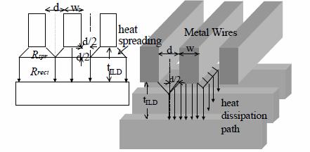
7 Examples (1) D L W Bulk Si FET SOI FET R TH 1 1 2k D 2k LW Si Si S R TH 1 t BOX 2W kbox ksitsi 1/2 k Si ~ 100 Wm -1 K -1 (highly doped Si) and D = 1 µm then R TH ~ 5 K/mW so T = PR TH ~ 5 K with 1 mw power t Si = 10 nm, t BOX = 50 nm, W = 1 µm k Si ~ 10 Wm -1 K -1 (reduced in thin film) and k BOX ~ 1.4 Wm -1 K -1 then R TH ~ 130 K/mW so T = PR TH ~ 67 K with 0.5 mw power 7
8 Examples (2) R B T L W t BOX = 90 nm, L = W = 1 µm and k BOX ~ 1.4 W/m/K TBR = thermal boundary resistance ~ 10-8 m 2 K/W R SiO2 t BOX R Si T 0 2D FET R B = TBR / (WL) ~ 10 K/mW R SiO2 = t BOX / (k BOX * WL) ~ 60 K/mW R Si = 1 / [2 * k Si * (W + t BOX )] ~ 4.5 K/mW total R TH ~ 75 K/mW so T = PR TH ~ 30 K with 0.4 mw power note the SiO 2 layer dominates, but TBR also plays an important role 8
 Equivalent thermal resistance R TH =")
9 Shape Factors Sunderland, ASHRAE (1964), many others Heat flux: q = Sk(T 1 -T 0 ) Equivalent thermal resistance R TH = 1/Sk 9
")
10 Many Shape Factors (Compact Models) 10
11 Obtaining the Temperature Distribution So far we ve only looked at lumped thermal models Now we want temperature distribution T(x) Simplest case: Si layer on SiO 2 /Si substrate (SOI) Or interconnect on thermally insulating SiO 2 11
 Energy In (here, Joule heat) = Energy Out (left, right, bottom) +")

12 1-D Interconnect with Heat Generation W L x x+dx d Heat: dt QAk dx dv I AJ A F A dx Electrical: SiO 2 Si T 0 t ox Write energy balance equation for element dx pick units of J or W (= J/s) Energy In (here, Joule heat) = Energy Out (left, right, bottom) + Change in Internal Energy ka ka hwdxt T QAdx T x x T x x dx 0 C( Adx) T t divide by (Adx): W Q kth T T0 C A e.g. J E if non-uniform or I 2 R/(WLd) if uniform convection-like term, here h = k ox /t ox and W/A = 1/d W can be perimeter if heat loss in all directions T t 12

13 Ex: 1D Rectangular Nanowire 1/m is natural length scale thermal healing length L H k k sub td sub 13

14 Interconnect Heat Loss and Crosstalk 14
 H ( 0 (a) Si t SI (b) dr p' I I dx 2 2 h 1 q 2 4 eff L H ka g Role of")
 g ox kox 8tox ln d 900 700 T max Role of thermal contact resistance et al. J. Appl. Phys.")
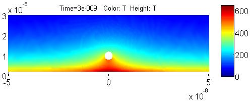
15 Ex: Carbon Nanotube (Cylinder) L T d A( kt ) p' g( T T0 ) 0 Pt g SiO 2 t OX T p' cosh( x / L H ) x) T 1 g cosh( L / 2L ) H ( 0 (a) Si t SI (b) dr p' I I dx 2 2 h 1 q 2 4 eff L H ka g Role of cylindrical heat spreading (shape factor!) g ox kox 8tox ln d T max Role of thermal contact resistance et al. J. Appl. Phys. 101, (2007) T (K) ΔT C X (m) dt ka dx C T R C CTh, 15
, http://dx.doi.org/10.1103/physrevlett.106.256801 C. Durkan et al.")
16 Further Reading L. Su et al., Measurement and modeling of self-heating in SOI nmosfets, IEEE Trans. Elec. Dev. 41, 69 (1994), A. Liao et al., "Thermally-Limited Current Carrying Ability of Graphene Nanoribbons," Phys. Rev. Lett. 106, (2011), C. Durkan et al., Analysis of failure mechanisms in electrically stressed Au nanowires, J. Appl. Phys. 86, 1280 (1999), D. Chen et al., Interconnect Thermal Modeling for Accurate Simulation of Circuit Timing and Reliability, IEEE Trans. CAD 19, 197 (2000), T.-Y. Chiang et al., Analytical Thermal Model for Multilevel VLSI Interconnects Incorporating Via Effect, IEEE EDL 23, 31 (2002), et al., Electrical and thermal transport in metallic single-wall carbon nanotubes on insulating substrates, J. Appl. Phys. 101, (2007), Energy Dissipation and Transport in Nanoscale Devices, Nano Research 3, 147 (2010), 16
Power and Heat: The Big Picture
 Power Power Density (W/cm 2 ) Power Dissipation in Nanoscale CMOS and Carbon Nanotubes Eric Pop Dept. of Electrical & Computer Engineering http://poplab.ece.uiuc.edu E. Pop 1 Power and Heat: The Big Picture
Electro-Thermal Transport in Silicon and Carbon Nanotube Devices E. Pop, D. Mann, J. Rowlette, K. Goodson and H. Dai
 Electro-Thermal Transport in Silicon and Carbon Nanotube Devices E. Pop, D. Mann, J. Rowlette, K. Goodson and H. Dai E. Pop, 1,2 D. Mann, 1 J. Rowlette, 2 K. Goodson 2 and H. Dai 1 Dept. of 1 Chemistry
Recap (so far) Low-Dimensional & Boundary Effects
 Low-Dimensional & Boundary Effects") Recap (so far) Ohm s & Fourier s Laws Mobility & Thermal Conductivity Heat Capacity Wiedemann-Franz Relationship Size Effects and Breakdown of Classical Laws 1 Low-Dimensional & Boundary Effects Energy
Recap (so far) Ohm s & Fourier s Laws Mobility & Thermal Conductivity Heat Capacity Wiedemann-Franz Relationship Size Effects and Breakdown of Classical Laws 1 Low-Dimensional & Boundary Effects Energy
Thermally-Limited Current Carrying Ability of Graphene Nanoribbons
 1 Thermally-Limited Current Carrying Ability of Graphene Nanoribbons Albert D. Liao 1,2,, Justin Z. Wu 3,4,, Xinran Wang 4, Kristof Tahy 5, Debdeep Jena 5, Hongjie Dai 4,*, Eric Pop 1,2,6,* 1 Dept. of
Thermal Management at Nanoscale: Problems and Opportunities
 Thermal Management at Nanoscale: Problems and Opportunities Alexander A. Balandin Nano-Device Laboratory Department of Electrical Engineering and Materials Science and Engineering Program University of
Simulation and Optimization of an In-plane Thermal Conductivity Measurement Structure for Silicon Nanostructures
 32nd International Thermal Conductivity Conference 20th International Thermal Expansion Symposium April 27 May 1, 2014 Purdue University, West Lafayette, Indiana, USA Simulation and Optimization of an
Thermally Limited Current Carrying Ability of Graphene Nanoribbons
 PRL 16, 5681 (11) P H Y S I C A L R E V I E W L E T T E R S week ending 4 JUNE 11 Thermally Limited Current Carrying Ability of Graphene Nanoribbons Albert D. Liao, 1, Justin Z. Wu, 3,4 Xinran Wang, 4
Chapter 2 HEAT CONDUCTION EQUATION
 Heat and Mass Transfer: Fundamentals & Applications 5th Edition in SI Units Yunus A. Çengel, Afshin J. Ghajar McGraw-Hill, 2015 Chapter 2 HEAT CONDUCTION EQUATION Mehmet Kanoglu University of Gaziantep
Thermal characterization of Au-Si multilayer using 3- omega method
 Thermal characterization of Au-Si multilayer using 3- omega method Sunmi Shin Materials Science and Engineering Program Abstract As thermal management becomes a serious issue in applications of thermoelectrics,
Introduction to Heat and Mass Transfer. Week 5
 Introduction to Heat and Mass Transfer Week 5 Critical Resistance Thermal resistances due to conduction and convection in radial systems behave differently Depending on application, we want to either maximize
Electrical and Thermal Transport in Metallic Single-Wall Carbon Nanotubes on Insulating Substrates
 Electrical and Thermal Transport in Metallic Single-Wall Carbon Nanotubes on Insulating Substrates Eric Pop, 1,2,* David A. Mann, 1 Kenneth E. Goodson 2 and Hongjie Dai 1 1 Laboratory for Advanced Materials
Supplementary Information. Characterization of nanoscale temperature fields during electromigration of nanowires
 Supplementary Information Characterization of nanoscale temperature fields during electromigration of nanowires Wonho Jeong,, Kyeongtae Kim,, *, Youngsang Kim,, Woochul Lee,, *, Pramod Reddy Department
Chapter 2 HEAT CONDUCTION EQUATION
 Heat and Mass Transfer: Fundamentals & Applications Fourth Edition Yunus A. Cengel, Afshin J. Ghajar McGraw-Hill, 2011 Chapter 2 HEAT CONDUCTION EQUATION Mehmet Kanoglu University of Gaziantep Copyright
Electrostatics of Nanowire Transistors
 Electrostatics of Nanowire Transistors Jing Guo, Jing Wang, Eric Polizzi, Supriyo Datta and Mark Lundstrom School of Electrical and Computer Engineering Purdue University, West Lafayette, IN, 47907 ABSTRACTS
Chapter 2: Heat Conduction Equation
 -1 General Relation for Fourier s Law of Heat Conduction - Heat Conduction Equation -3 Boundary Conditions and Initial Conditions -1 General Relation for Fourier s Law of Heat Conduction (1) The rate of
Lecture 6: 2D FET Electrostatics
 Lecture 6: 2D FET Electrostatics 2016-02-01 Lecture 6, High Speed Devices 2014 1 Lecture 6: III-V FET DC I - MESFETs Reading Guide: Liu: 323-337 (he mainly focuses on the single heterostructure FET) Jena:
This article has been accepted and published on J-STAGE in advance of copyediting. Content is final as presented.
 This article has been accepted and published on J-STAGE in advance of copyediting. Content is final as presented. References IEICE Electronics Express, Vol.* No.*,*-* Effects of Gamma-ray radiation on
Resistance Thermometry based Picowatt-Resolution Heat-Flow Calorimeter
 Resistance Thermometry based Picowatt-Resolution Heat-Flow Calorimeter S. Sadat 1, E. Meyhofer 1 and P. Reddy 1, 1 Department of Mechanical Engineering, University of Michigan, Ann Arbor, 48109 Department
VLSI Design and Simulation
 VLSI Design and Simulation Performance Characterization Topics Performance Characterization Resistance Estimation Capacitance Estimation Inductance Estimation Performance Characterization Inverter Voltage
ELEC9712 High Voltage Systems. 1.2 Heat transfer from electrical equipment
 ELEC9712 High Voltage Systems 1.2 Heat transfer from electrical equipment The basic equation governing heat transfer in an item of electrical equipment is the following incremental balance equation, with
Heat Sink Design and Temperature Distribution Analysis for Millimeter Wave IMPATT Oscillators using Finite Difference Method
 Available online at www.scholarsresearchlibrary.com Archives of Applied Science Research, 2011, 3 (2):107-120 (http://scholarsresearchlibrary.com/archive.html) ISSN 0975-508X CODEN (USA) AASRC9 Heat Sink
Supporting Online Material for
 www.sciencemag.org/cgi/content/full/science.11938/dc1 Supporting Online Material for Low Power Switching of Phase-Change Materials with Carbon Nanotube Electrodes Feng Xiong, lbert Liao, David Estrada,
Pin Fin Lab Report Example. Names. ME331 Lab
 Pin Fin Lab Report Example Names ME331 Lab 04/12/2017 1. Abstract The purposes of this experiment are to determine pin fin effectiveness and convective heat transfer coefficients for free and forced convection
There's Plenty of Room at the Bottom
 There's Plenty of Room at the Bottom 12/29/1959 Feynman asked why not put the entire Encyclopedia Britannica (24 volumes) on a pin head (requires atomic scale recording). He proposed to use electron microscope
Thermal Unit Operation (ChEg3113)
") Thermal Unit Operation (ChEg3113) Lecture 3- Examples on problems having different heat transfer modes Instructor: Mr. Tedla Yeshitila (M.Sc.) Today Review Examples Multimode heat transfer Heat exchanger
Thermal Unit Operation (ChEg3113) Lecture 3- Examples on problems having different heat transfer modes Instructor: Mr. Tedla Yeshitila (M.Sc.) Today Review Examples Multimode heat transfer Heat exchanger
AC Electrothermal Characterization of Doped-Si Heated Microcantilevers Using Frequency-Domain Finite Element Analysis
 AC Electrothermal Characterization of Doped-Si Heated Microcantilevers Using Frequency-Domain Finite Element Analysis K. Park 1, S. Hamian 1, A. M. Gauffreau 2, T. Walsh 2 1 University of Utah, Salt Lake
Size-dependent Metal-insulator Transition Random Materials Crystalline & Amorphous Purely Electronic Switching
 Nanometallic RRAM I-Wei Chen Department of Materials Science and Engineering University of Pennsylvania Philadelphia, PA 19104 Nature Nano, 6, 237 (2011) Adv Mater,, 23, 3847 (2011) Adv Func Mater,, 22,
MOSFET: Introduction
 E&CE 437 Integrated VLSI Systems MOS Transistor 1 of 30 MOSFET: Introduction Metal oxide semiconductor field effect transistor (MOSFET) or MOS is widely used for implementing digital designs Its major
A RIDGE WAVEGUIDE FOR THERMO-OPTIC APPLICATION
 Progress In Electromagnetics Research Letters, Vol. 6, 1 9, 2009 A RIDGE WAVEGUIDE FOR THERMO-OPTIC APPLICATION A. M. Al-Hetar, A. S. M. Supa at, and A. B. Mohammad Photonics Technology Center (PTC) Faculty
Electrical and thermal transport in metallic single-wall carbon nanotubes on insulating substrates
 JOURNAL OF APPLIED PHYSICS 101, 093710 2007 Electrical and thermal transport in metallic single-wall carbon nanotubes on insulating substrates Eric Pop a Laboratory for Advanced Materials and Department
A Bottom-gate Depletion-mode Nanowire Field Effect Transistor (NWFET) Model Including a Schottky Diode Model
 Model Including a Schottky Diode Model") Journal of the Korean Physical Society, Vol. 55, No. 3, September 2009, pp. 1162 1166 A Bottom-gate Depletion-mode Nanowire Field Effect Transistor (NWFET) Model Including a Schottky Diode Model Y. S.
Journal of the Korean Physical Society, Vol. 55, No. 3, September 2009, pp. 1162 1166 A Bottom-gate Depletion-mode Nanowire Field Effect Transistor (NWFET) Model Including a Schottky Diode Model Y. S.
Thermal Transport in Graphene and other Two-Dimensional Systems. Li Shi. Department of Mechanical Engineering & Texas Materials Institute
 Thermal Transport in Graphene and other Two-Dimensional Systems Li Shi Department of Mechanical Engineering & Texas Materials Institute Outline Thermal Transport Theories and Simulations of Graphene Raman
Managing. heat for electronics by Patrick K. Schelling 1, *, Li Shi 2, and Kenneth E. Goodson 3
 Managing heat for electronics by Patrick K. Schelling 1, *, Li Shi 2, and Kenneth E. Goodson 3 Increasing power densities and decreasing transistor dimensions are hallmarks of modern computer chips. Both
AN ANALYTICAL THERMAL MODEL FOR THREE-DIMENSIONAL INTEGRATED CIRCUITS WITH INTEGRATED MICRO-CHANNEL COOLING
 THERMAL SCIENCE, Year 2017, Vol. 21, No. 4, pp. 1601-1606 1601 AN ANALYTICAL THERMAL MODEL FOR THREE-DIMENSIONAL INTEGRATED CIRCUITS WITH INTEGRATED MICRO-CHANNEL COOLING by Kang-Jia WANG a,b, Hong-Chang
Supporting Information
 Supporting Information Monolithically Integrated Flexible Black Phosphorus Complementary Inverter Circuits Yuanda Liu, and Kah-Wee Ang* Department of Electrical and Computer Engineering National University
Thermal Phenomena in Nanoscale Transistors
 Eric Pop Department of Electrical Engineering, Stanford University, Stanford, CA 94305 Kenneth E. Goodson Department of Mechanical Engineering, Stanford University, Stanford, CA 94305 e-mail: goodson@stanford.edu
Emerging Interconnect Technologies for CMOS and beyond-cmos Circuits
 Emerging Interconnect Technologies for CMOS and beyond-cmos Circuits Sou-Chi Chang, Rouhollah M. Iraei Vachan Kumar, Ahmet Ceyhan and Azad Naeemi School of Electrical & Computer Engineering Georgia Institute
Report on 7th US-Japan Joint Seminar on Nanoscale Transport Phenomena Science and Engineering
 Report on 7th US-Japan Joint Seminar on Nanoscale Transport Phenomena Science and Engineering December 11-14, 2011, Shima, Japan co-chairs: Shigeo Maruyama, Kazuyoshi Fushinobu, Jennifer Lukes, Li Shi
CMOS Scaling. Two motivations to scale down. Faster transistors, both digital and analog. To pack more functionality per area. Lower the cost!
 Two motivations to scale down CMOS Scaling Faster transistors, both digital and analog To pack more functionality per area. Lower the cost! (which makes (some) physical sense) Scale all dimensions and
Chapter 3: Steady Heat Conduction
 3-1 Steady Heat Conduction in Plane Walls 3-2 Thermal Resistance 3-3 Steady Heat Conduction in Cylinders 3-4 Steady Heat Conduction in Spherical Shell 3-5 Steady Heat Conduction with Energy Generation
Chapter 5 Time-Dependent Conduction
 Chapter 5 Time-Dependent Conduction 5.1 The Lumped Capacitance Method This method assumes spatially uniform solid temperature at any instant during the transient process. It is valid if the temperature
Supplementary Figure S1. AFM images of GraNRs grown with standard growth process. Each of these pictures show GraNRs prepared independently,
 Supplementary Figure S1. AFM images of GraNRs grown with standard growth process. Each of these pictures show GraNRs prepared independently, suggesting that the results is reproducible. Supplementary Figure
Quantum Mechanical Simulation for Ultra-thin High-k Gate Dielectrics Metal Oxide Semiconductor Field Effect Transistors
 Mechanical Simulation for Ultra-thin High-k Gate Dielectrics Metal Oxide Semiconductor Field Effect Transistors Shih-Ching Lo 1, Yiming Li 2,3, and Jyun-Hwei Tsai 1 1 National Center for High-Performance
Energy Dissipation and Transport in Nanoscale Devices
 Nano Res (2010) 3: 147 169 1 DOI 10.1007/s12274-010-1019-z Review Article Energy Dissipation and Transport in Nanoscale Devices Eric Pop ( ) Department of Electrical and Computer Engineering, Micro and
Chapter 3: Steady Heat Conduction. Dr Ali Jawarneh Department of Mechanical Engineering Hashemite University
 Chapter 3: Steady Heat Conduction Dr Ali Jawarneh Department of Mechanical Engineering Hashemite University Objectives When you finish studying this chapter, you should be able to: Understand the concept
Capacitance-Voltage characteristics of nanowire trigate MOSFET considering wave functionpenetration
 Global Journal of researches in engineering Electrical and electronics engineering Volume 12 Issue 2 Version 1.0 February 2012 Type: Double Blind Peer Reviewed International Research Journal Publisher:
Chapter 2: Steady Heat Conduction
 2-1 General Relation for Fourier s Law of Heat Conduction 2-2 Heat Conduction Equation 2-3 Boundary Conditions and Initial Conditions 2-4 Variable Thermal Conductivity 2-5 Steady Heat Conduction in Plane
Thermal Management for LED Applications
 Thermal Management for LED Applications What is the role of the PCB? http://saturnelectronics.com/thermal_pcb_design_led_signup.htm Presented by Clemens Lasance Clemens is a former Principal Scientist
Scaling Issues in Planar FET: Dual Gate FET and FinFETs
 Scaling Issues in Planar FET: Dual Gate FET and FinFETs Lecture 12 Dr. Amr Bayoumi Fall 2014 Advanced Devices (EC760) Arab Academy for Science and Technology - Cairo 1 Outline Scaling Issues for Planar
Homework Week 3: Nanoscale and macroscale characterization Thermoelectricity: From Atoms to Systems
 Homework Week 3: Nanoscale and macroscale characterization Thermoelectricity: From Atoms to Systems Je-Hyeong Bahk and Ali Shakouri nanohub-u Fall 2013 Answer the thirteen questions including all the sub-questions
LECTURE 3 MOSFETS II. MOS SCALING What is Scaling?
 LECTURE 3 MOSFETS II Lecture 3 Goals* * Understand constant field and constant voltage scaling and their effects. Understand small geometry effects for MOS transistors and their implications modeling and
A Verilog-A Compact Model for Negative Capacitance FET
 A Verilog-A Compact Model for Negative Capacitance FET Version.. Muhammad Abdul Wahab and Muhammad Ashraful Alam Purdue University West Lafayette, IN 4797 Last Updated: Oct 2, 25 Table of Contents. Introduction...
New Functions. Test mode and Specimen failure. Power cycle test system with thermal analysis capability using structure function.
 using structure function. (1) Page 1/5 Test mode and failure There are two modes in a power cycle test: Tj Power cycle that changes the junction temperature (Tj Temperature) inside of the power semiconductor
University of Rome Tor Vergata
 University of Rome Tor Vergata Faculty of Engineering Department of Industrial Engineering THERMODYNAMIC AND HEAT TRANSFER HEAT TRANSFER dr. G. Bovesecchi gianluigi.bovesecchi@gmail.com 06-7259-727 (7249)
One-Dimensional, Steady-State. State Conduction without Thermal Energy Generation
 One-Dimensional, Steady-State State Conduction without Thermal Energy Generation Methodology of a Conduction Analysis Specify appropriate form of the heat equation. Solve for the temperature distribution.
Heat Removal of a Protection Chip after Surge Pulse Tom Graf Hochschule Luzern T&A Technikumstrasse 21 CH-6048 Horw Switzerland
 Heat Removal of a Protection Chip after Surge Pulse Tom Graf Hochschule Luzern T&A Technikumstrasse 21 CH-6048 Horw Switzerland 1 / 23 Abstract EMC protection elements experienced significant heating after
Thermo-structural Model of Stacked Field-programmable Gate Arrays (FPGAs) with Through-silicon Vias (TSVs)
 with Through-silicon Vias (TSVs)") Manuscript for Review Thermo-structural Model of Stacked Field-programmable Gate Arrays (FPGAs) with Through-silicon Vias (TSVs) Journal: Electronics Letters Manuscript ID: draft Manuscript Type: Letter
Manuscript for Review Thermo-structural Model of Stacked Field-programmable Gate Arrays (FPGAs) with Through-silicon Vias (TSVs) Journal: Electronics Letters Manuscript ID: draft Manuscript Type: Letter
Experimental Study on Interfacial Thermal Transport of Multi-Walled Carbon Nanotube
 Experimental Study on Interfacial Thermal Transport of Multi-Walled Carbon Nanotube KOJI TAKAHASHI 1, 2, 3), JUN HIROTANI 1), YUTAKA YAMADA 1) 1) Department of Aeronautics and Astronautics 2) JST, CREST
Electronic Supplementary Information (ESI)
") Electronic Supplementary Material (ESI) for Nanoscale. This journal is The Royal Society of Chemistry 2015 Electronic Supplementary Information (ESI) Thermal Conductivity Measurements of High and Low Thermal
Electronic Supplementary Material (ESI) for Nanoscale. This journal is The Royal Society of Chemistry 2015 Electronic Supplementary Information (ESI) Thermal Conductivity Measurements of High and Low Thermal
BACKEND IMPLICATIONS FOR THERMAL EFFECTS IN 3D INTEGRATED SOI STRUCTURES
 BACKEND IMPLICATIONS FOR THERMAL EFFECTS IN 3D INTEGRATED SOI STRUCTURES D. Celo, R. Joshi 1, and T. Smy Dept. of Electronics, Carleton University, Ottawa, ON, Canada K1S 5B6, ph: 613-520-3967, fax: 613-520-5708:
Supporting Information. by Hexagonal Boron Nitride
 Supporting Information High Velocity Saturation in Graphene Encapsulated by Hexagonal Boron Nitride Megan A. Yamoah 1,2,, Wenmin Yang 1,3, Eric Pop 4,5,6, David Goldhaber-Gordon 1 * 1 Department of Physics,
Non-Continuum Energy Transfer: Overview
 Non-Continuum Energy Transfer: Overview D. B. Go Slide 1 Topics Covered To Date Conduction - transport of thermal energy through a medium (solid/ liquid/gas) due to the random motion of the energy carriers
Carbon Nanotubes for Interconnect Applications Franz Kreupl, Andrew P. Graham, Maik Liebau, Georg S. Duesberg, Robert Seidel, Eugen Unger
 Carbon Nanotubes for Interconnect Applications Franz Kreupl, Andrew P. Graham, Maik Liebau, Georg S. Duesberg, Robert Seidel, Eugen Unger Infineon Technologies Corporate Research Munich, Germany Outline
Nanocarbon Technology for Development of Innovative Devices
 Nanocarbon Technology for Development of Innovative Devices Shintaro Sato Daiyu Kondo Shinichi Hirose Junichi Yamaguchi Graphene, a one-atom-thick honeycomb lattice made of carbon, and a carbon nanotube,
Ming-C. Cheng: Research overview
 Ming-C. Cheng: Research overview Dept. of Electrical & Computer Engineering Clarkson University. Potsdam, NY, mcheng@clarkson.edu Research Experiences Block-Based Reduced Order Thermal Modeling for semiconductor
Manufacture of Nanostructures for Power Electronics Applications
 Manufacture of Nanostructures for Power Electronics Applications Brian Hunt and Jon Lai Etamota Corporation 2672 E. Walnut St. Pasadena, CA 91107 APEC, Palm Springs Feb. 23rd, 2010 1 Background Outline
Proposed Thermal Circuit Model for the Cost Effective Design of Fin FET
 Proposed Thermal Circuit Model for the Cost Effective Design of Fin FET Abstract A K M Kamrul Hasan, MD. Nizamul Islam, Dewan Siam Shafiullah Islamic University of Technology (IUT) Gazipur, Bangladesh.
SUPPLEMENTARY INFORMATION
 Engineered doping of organic semiconductors for enhanced thermoelectric efficiency G.-H. Kim, 1 L. Shao, 1 K. Zhang, 1 and K. P. Pipe 1,2,* 1 Department of Mechanical Engineering, University of Michigan,
EE115C Winter 2017 Digital Electronic Circuits. Lecture 3: MOS RC Model, CMOS Manufacturing
 EE115C Winter 2017 Digital Electronic Circuits Lecture 3: MOS RC Model, CMOS Manufacturing Agenda MOS Transistor: RC Model (pp. 104-113) S R on D CMOS Manufacturing Process (pp. 36-46) S S C GS G G C GD
Quiz #1 Practice Problem Set
 Name: Student Number: ELEC 3908 Physical Electronics Quiz #1 Practice Problem Set? Minutes January 22, 2016 - No aids except a non-programmable calculator - All questions must be answered - All questions
Use of Multi-Walled Carbon Nanotubes for UV radiation detection
 Use of Multi-Walled Carbon Nanotubes for UV radiation detection Viviana Carillo 11th Topical Seminar on Innovative Particle and Radiation Detectors (IPRD08) 1-4 October 2008 Siena, Italy A new nanostructured
Xing Sheng, 微纳光电子材料与器件工艺原理. Doping 掺杂. Xing Sheng 盛兴. Department of Electronic Engineering Tsinghua University
 微纳光电子材料与器件工艺原理 Doping 掺杂 Xing Sheng 盛兴 Department of Electronic Engineering Tsinghua University xingsheng@tsinghua.edu.cn 1 Semiconductor PN Junctions Xing Sheng, EE@Tsinghua LEDs lasers detectors solar
ELECTROMAGNETIC MODELING OF THREE DIMENSIONAL INTEGRATED CIRCUITS MENTOR GRAPHICS
 ELECTROMAGNETIC MODELING OF THREE DIMENSIONAL INTEGRATED CIRCUITS MENTOR GRAPHICS H I G H S P E E D D E S I G N W H I T E P A P E R w w w. m e n t o r. c o m / p c b INTRODUCTION Three Dimensional Integrated
EECS130 Integrated Circuit Devices
 EECS130 Integrated Circuit Devices Professor Ali Javey 10/30/2007 MOSFETs Lecture 4 Reading: Chapter 17, 19 Announcements The next HW set is due on Thursday. Midterm 2 is next week!!!! Threshold and Subthreshold
SILICON-ON-INSULATOR (SOI) technology has been regarded
 technology has been regarded") IEEE TRANSACTIONS ON ELECTRON DEVICES, VOL. 53, NO. 10, OCTOBER 2006 2559 Analysis of the Gate Source/Drain Capacitance Behavior of a Narrow-Channel FD SOI NMOS Device Considering the 3-D Fringing Capacitances
IEEE TRANSACTIONS ON ELECTRON DEVICES, VOL. 53, NO. 10, OCTOBER 2006 2559 Analysis of the Gate Source/Drain Capacitance Behavior of a Narrow-Channel FD SOI NMOS Device Considering the 3-D Fringing Capacitances
Thermal Systems. Basic Modeling Elements. Interconnection Relationships. Derive Input/Output Models. Resistance. Capacitance
 hermal Systems Basic Modeling Elements Resistance Conduction Convection Radiation Capacitance Interconnection Relationships Energy Balance - 1st Law of hermodynamics Derive Input/Output Models ME375 hermal
CALCULATION of the mean or centroidal value of discrete
 636 IEEE TRANSACTIONS ON COMPONENTS AND PACKAGING TECHNOLOGIES, VOL 29, NO 3, SEPTEMBER 2006 Influence Coefficient Method for Calculating Discrete Heat Source Temperature on Finite Convectively Cooled
 PROBLEM 3.10 KNOWN: Dimensions and surface conditions of a plate thermally joined at its ends to heat sinks at different temperatures. FIND: (a) Differential equation which determines temperature distribution
Conduction Heat Transfer. Fourier Law of Heat Conduction. x=l Q x+ Dx. insulated x+ Dx. x x. x=0 Q x A
 Conduction Heat Transfer Reading Problems 10-1 10-6 10-20, 10-48, 10-59, 10-70, 10-75, 10-92 10-117, 10-123, 10-151, 10-156, 10-162 11-1 11-2 11-14, 11-20, 11-36, 11-41, 11-46, 11-53, 11-104 Fourier Law
PROBLEM 1.2 ( ) 25 C 15 C dx L 0.30 m Ambient air temperature, T2 (C)
 25 C 15 C dx L 0.30 m Ambient air temperature, T2 (C)") PROBLEM 1.2 KNOWN: Inner surface temperature and thermal conductivity of a concrete wall. FIND: Heat loss by conduction through the wall as a function of ambient air temperatures ranging from -15 to 38
PROBLEM 1.2 KNOWN: Inner surface temperature and thermal conductivity of a concrete wall. FIND: Heat loss by conduction through the wall as a function of ambient air temperatures ranging from -15 to 38
Chapter 2 The Well 9/5/2017. E E 480 Introduction to Analog and Digital VLSI Paul M. Furth New Mexico State University
 hapter 2 The Well E E 480 Introduction to Analog and Digital VLSI Paul M. Furth New Mexico State University p+ sub ~ 150 m thick, p-epi ~ 30 m thick All transistors go in p- epi layer Typical p- doping
Elementary Process of Electromigration at Metallic Nanojunctions in the Ballistic Regime
 Elementary Process of Electromigration at Metallic Nanojunctions in the Ballistic Regime Kaz Hirakawa Institute of Industrial Science, University of Tokyo CREST, JST collaborators: Akinori Umeno, Kenji
Strong-electric-field effects and antenna resonances in single-wall carbon nanotube films
 Strong-electric-field effects and antenna resonances in single-wall carbon nanotube films Dalius Seliuta Center for Physical Sciences and Technology, Vilnius, Lithuania Liudas Subačius, Irmantas Kašalynas,
Modelling of Diamond Devices with TCAD Tools
 RADFAC Day - 26 March 2015 Modelling of Diamond Devices with TCAD Tools A. Morozzi (1,2), D. Passeri (1,2), L. Servoli (2), K. Kanxheri (2), S. Lagomarsino (3), S. Sciortino (3) (1) Engineering Department
Carbon Nanotubes in Interconnect Applications
 Carbon Nanotubes in Interconnect Applications Page 1 What are Carbon Nanotubes? What are they good for? Why are we interested in them? - Interconnects of the future? Comparison of electrical properties
COMPARATIVE ANALYSIS OF CARBON NANOTUBES AS VLSI INTERCONNECTS
 International Journal of Science, Engineering and Technology Research (IJSETR), Volume 4, Issue 8, August 15 COMPARATIVE ANALYSIS OF CARBON NANOTUBES AS VLSI INTERCONNECTS Priya Srivastav, Asst. Prof.
3/10/2013. Lecture #1. How small is Nano? (A movie) What is Nanotechnology? What is Nanoelectronics? What are Emerging Devices?
 What is Nanotechnology? What is Nanoelectronics? What are Emerging Devices?") EECS 498/598: Nanocircuits and Nanoarchitectures Lecture 1: Introduction to Nanotelectronic Devices (Sept. 5) Lectures 2: ITRS Nanoelectronics Road Map (Sept 7) Lecture 3: Nanodevices; Guest Lecture by
EECS 498/598: Nanocircuits and Nanoarchitectures Lecture 1: Introduction to Nanotelectronic Devices (Sept. 5) Lectures 2: ITRS Nanoelectronics Road Map (Sept 7) Lecture 3: Nanodevices; Guest Lecture by
Chapter 2: Heat Conduction. Dr Ali Jawarneh Department of Mechanical Engineering, Hashemite University
 Chapter : Heat Conduction Equation Dr Ali Jawarneh Department of Mechanical Engineering, Hashemite University Objectives When you finish studying this chapter, you should be able to: Understand multidimensionality
ENHANCEMENT OF NANO-RC SWITCHING DELAY DUE TO THE RESISTANCE BLOW-UP IN InGaAs
 NANO: Brief Reports and Reviews Vol. 2, No. 4 (27) 233 237 c World Scientific Publishing Company ENHANCEMENT OF NANO-RC SWITCHING DELAY DUE TO THE RESISTANCE BLOW-UP IN InGaAs MICHAEL L. P. TAN, ISMAIL
RADIATION EFFECTS IN SEMICONDUCTOR MATERIALS AND DEVICES FOR SPACE APPLICATIONS. Cor Claeys and Eddy Simoen
 RADIATION EFFECTS IN SEMICONDUCTOR MATERIALS AND DEVICES FOR SPACE APPLICATIONS Cor Claeys and Eddy Simoen IMEC 2010 OUTLINE Introduction Total Dose Effects in thin gate oxides RILC, RSB, SEGR, Latent
Numerical Heat and Mass Transfer
 Master degree in Mechanical Engineering Numerical Heat and Mass Transfer 02-Transient Conduction Fausto Arpino f.arpino@unicas.it Outline Introduction Conduction ü Heat conduction equation ü Boundary conditions
Local Joule Heating and Overall Resistance Increase
 Journal in oid-containing of ELECTRONIC MATERIALS, Aluminum ol. 30, Interconnects No. 4, 2001 367 Special Issue Paper Local Joule Heating and Overall Resistance Increase in oid-containing Aluminum Interconnects
Carbon Nanotube Electronics
 Carbon Nanotube Electronics Jeorg Appenzeller, Phaedon Avouris, Vincent Derycke, Stefan Heinz, Richard Martel, Marko Radosavljevic, Jerry Tersoff, Shalom Wind H.-S. Philip Wong hspwong@us.ibm.com IBM T.J.
UNIVERSITY OF WATERLOO. ECE 309 Thermodynamics and Heat Transfer. Final Examination Spring 1997
 UNIVERSITY OF WATERLOO DEPARTMENT OF ELECTRICAL ENGINEERING ECE 309 Thermodynamics and Heat Transfer Final Examination Spring 1997 M.M. Yovanovich August 5, 1997 9:00 A.M.-12:00 Noon NOTE: 1. Open book
Graphene devices and integration: A primer on challenges
 Graphene devices and integration: A primer on challenges Archana Venugopal (TI) 8 Nov 2016 Acknowledgments: Luigi Colombo (TI) UT Dallas and UT Austin 1 Outline Where we are Issues o Contact resistance
Introduction of Nano Science and Tech. Thermal and Electric Conduction in Nanostructures. Nick Fang
 Introduction of Nano Science and Tech Thermal and Electric Conduction in Nanostructures Nick Fang Course Website: nanohub.org Compass.illinois.edu ME 498 2006-09 Nick Fang, University of Illinois. All
Thermal Oxidation of Si
 Thermal Oxidation of General Properties of O 2 Applications of thermal O 2 Deal-Grove Model of Oxidation Thermal O 2 is amorphous. Weight Density = 2.20 gm/cm 3 Molecular Density = 2.3E22 molecules/cm
12/21/2014 7:39 PM. Chapter 2. Energy and the 1st Law of Thermodynamics. Dr. Mohammad Suliman Abuhaiba, PE
 Chapter 2 Energy and the 1st Law of Thermodynamics 1 2 Homework Assignment # 2 Problems: 1, 7, 14, 20, 30, 36, 42, 49, 56 Design and open end problem: 2.1D Due Monday 22/12/2014 3 Work and Kinetic Energy
Australian Journal of Basic and Applied Sciences. Numerical Investigation of Flow Boiling in Double-Layer Microchannel Heat Sink
 AENSI Journals Australian Journal of Basic and Applied Sciences ISSN:1991-8178 Journal home page: www.ajbasweb.com Numerical Investigation of Flow Boiling in Double-Layer Microchannel Heat Sink Shugata
Boundary Condition Dependency
 Boundary Condition Dependency of Junction to Case Thermal Resistance Introduction The junction to case ( ) thermal resistance of a semiconductor package is a useful and frequently utilized metric in thermal