Random Walk. to Graphene
|
|
|
- Lewis Harris
- 5 years ago
- Views:
Transcription


1 Random Walk Manchester Nottingham Bath 1992 Stockholm 2010 Copenhagen 1991 Moscow Nijmegen to Graphene STORY BEHIND Chernogolovka Sochi timeline: from 1987 to Science 2004 starting with stories irrelevant to graphene but relevant to a bigger picture Nalchik


2 PhD 1987 Investigation of mechanisms of transport relaxation in metals by a helicon resonance method message I took away: NEVER TORTURE STUDENTS WITH BORING/DEAD PROJECTS! as exciting as it sounds

3 SWEET TASTE OF FREEDOM staff scientist in Chernogolovka: something new but still possible with available Soviet facilities diffusive ballistic magnetic field inhomogeneous on a submicron scale experience I took away: NEW EXPERIMENTAL SYSTEM IS BETTER THAN A NEW PHENOMENON! Geim, JETP Lett Geim, Sergey Dubonos et al JETP Lett later, two PRL 1991, 1994


4 MOVING YEARS postdocs in Nottingham x2, Bath & Copenhagen: age =32 h-index ~1 SEMICONDUCTOR PHYSICS my first 6-month visit submicron GaAs wires from a drawer Geim, Laurence Eaves, Peter Main et al Phys. Rev. Lett Phys. Rev. Lett GaAlAs heterostructures universal conductance fluctuations resonant tunnelling phenomena quantum point contacts quantum Hall effect 2DEG in periodic potentials experience to tease colleagues: NO SUCH THING AS BAD SAMPLES, ONLY BAD POSTDOCS

5 micron-sized Hall probes to investigate superconductors, ferromagnetics, etc GOING DUTCH associate professor in Nijmegen: FINDING RESEARCH NICHE: possible but somewhat different MESOSCOPIC SUPERCONDUCTIVITY paramagnetic Meissner effect T > T C T < T C fractional flux vortices & vortex shells structures from Nottingham lithography in Russia: Sergey Dubonos measurements in Nijmegen writing up with Irina Grigorieva: Nature 390, 259 (1997); Nature 396, 144 (1998); Nature 407, 55 (2000); PRL 79, 4653 (1997); PRL 85, 1528 (2000)


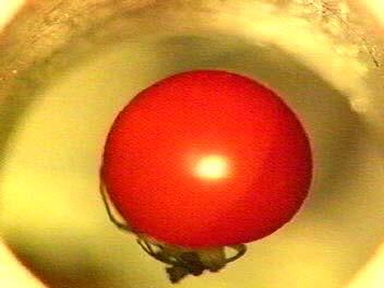
6 FRIDAY NIGHT EXPERIMENTS water in high magnetic fields? starting 1997 magnetic water descaler ancient magnets: consume a lot of energy require extra cryostats

7 A BIT OF LEVITY water in high magnetic fields

8 NEEDS EMPHASIS Nature 1991

9 KNOWLEDGE IS FUN

10 WOW! FACTOR

11

12 PERCEPTION CHANGE everything (and everybody) is magnetic; ever present diamagnetism is NOT negligible messages to take away: LOOK FOR COMPETITIVE EDGE even obsolete facilities may offer some in many textbooks sideline experience of the IgNobel Prize: DON T TAKE YOURSELF TOO SERIOUSLY

 Au probes on top of 2DEG rings 2 µm 1 µm")
 by 2003: well-equipped lab and")

13 MANCUNIAN WAY chair in Manchester: 2001 present empty lab; little start-up; no central microfabrication FIRST ESTABLISH YOURSELF & SET UP NEW FACILITIES microfabrication still in Russia (Dubonos) Au probes on top of 2DEG rings 2 µm 1 µm Kostya Novoselov et al, Nature 426, 812 (2003) Irina Grigorieva et al, PRL 92, (2004) by 2003: well-equipped lab and state-of-the-art microfabrication thanks to EPSRC & University H 2DEG-ferromagnetic- -superconducting hybrid I subatomic movements of domain walls V

14 FRIDAY NIGHTS in MANCHESTER HOW COMES THAT GECKO CAN CLIMB WALLS?


15 FRIDAY NIGHTS in MANCHESTER sticky feet: geckos climb due to their hairy toes PNAS 2002 courtesy of K Autumn submicron size (!) - standard spatial scale in our work


16 GECKO TAPE proof of concept: biomimetic dry adhesive based on gecko principle PLACING EMPHASIS Geim, Sergey Dubonos, Irina Grigorieva, Kostya Novoselov et al Nature Materials 2003
17 FRIDAY NIGHT FAILURES magnetic water 3 different attempts Sergey Morozov permeability of high-t c superconductor to oxygen Jeroen Meessen in Nijmegen high-t c superconductivity in NiAs+FeSe alloys Lamarches samples (EPL 2000) well before the discovery of pnictide superconductivity detection of heart beats of individual yeast cells (Irina Barbolina, Kostya Novoselov et al APL 2006) experience I am still mulling over: FAILURES ARE NOT AS OFTEN AS ONE CAN EXPECT

18 BRIEF HISTORY OF GRAPHENE

19 One Little Thought Cloud metallic electronics Schlesinger 2000 Lemanov & Kholkin 1994 Petrashov 1991 Bose (1906) Mott (1902) mostly, Bi changes ~1% E electric breakdown ~1V/nm max induced concentration cm -2 change the number of electrons -> change conductivity single atomic layer of a metal cm -2 rarely stable for thickness below 100 Å
20 One Little Thought Cloud MANY MANY DIFFERENT EPITAXIAL SYSTEMS ~few nm thick Al grown by MBE on top of GaAlAs from Nottingham metallic electronics Schlesinger 2000 Lemanov & Kholkin 1994 Petrashov 1991 Bose (1906) Mott (1902) tinkering for >10 years with the following idea WOULD IT BE STABLE, OR MELT AND OXIDIZE? chemically remove the substrate ultra-thin monocrystal

21 Two More Little Clouds metallic electronics Schlesinger 2000 Lemanov & Kholkin 1994 Petrashov 1991 Bose (1906) Mott (1902) carbon nanotube transistors Ijima, Ebbesen, McEuen Dekker, Avouris Dresselhauses review 1981 little known about thin films of graphite Esquinazi & Kopelevich


22 THE LEGEND OF SCOTCH TAPE 2002 PhD project of Da Jiang: make graphite films as thin as possible and study their mesoscopic properties including electric field effect & metallic transistor Oleg Shklyarevskii s idea ~2.5 cm HOPG vs HDPG optical image polishing is dead, long live Scotch tape! graphite flakes on cellotape


23 UNTIL A SINGLE LAYER FOUND AFM a few months later SHOCK for INTUITION background as of 2004: thin film deposition & semiconductor physics incl MBE 5x5 µm 2 a few years later seen by a naked eye next to impossible to grow monolayers 1 mm Venables, Spiller, Hanbucken Rep Prog Phys 1984 Komnik Physics of Metal Films 1979

24 2D GROWTH IS FORBIDDEN 400 carbon atoms at 2000 K Fasolino (Nijmegen) growth means temperature close to melting causes violent vibrations destroys order in 2D Peierls; Landau; Mermin-Wagner; (only nm-scale flat crystals are possible to grow in isolation)

25 THERMODYNAMIC STABILITY graphene sheets should scroll Kaner Science 2003 Braga et al Nanolett 2004 graphene: thermodynamically unstable for <24,000 atoms or size < 20 nm Shenderova, Zhirnov, Brenner Crit Rev Mat Sci 2002 THERMODYNAMICALLY UNSTABLE does not mean IMPOSSIBLE -JUST METASTABLE-
26 GRAPHENE VIA 3D GROWTH


 Nature")


27 HISTORY OF GRAPHENE nanosrolls free growth substrate growth STM TEM graphene on metal: Land et al Surf Sci 1992 Shioyama JMSL 2001 Kaner Science 2003 Ebbessen (~60 layers) Nature 1997, APL 2001 graphene on graphite: Enoki Chem. Phys. Lett J Phys 2002 as cited in our first paper in 2004


 STM AFM proof of isolated graphene")


28 HISTORY OF GRAPHENE intercalation Frindt Science 1989 Horiuchi et al APL 2004 TEM cleavage Kurtz PRB 1990 Ebbesen Adv Mat 1995 SEM substrate growth Grant Surf Sci 1970 (on Ru/Rh) Bommel Surf Sci 1975 (SiC) STM AFM proof of isolated graphene added along the same lines in our 2007 review Ohashi Tanso 1997 Ruoff APL 1999 Gan Surf Sci 2003 LEED McConville PRB 1986 Nagashima Surf Sci 1993 Forbeaux PRB 1998


29 DISCOVERY OF GRAPHENE -OBLIVIONdigging through old literature Benjamin Brodie Phil Trans carbonic acid Graphon 33 suspension of graphene oxide crystallites TEM studies of the dry residue Ruess & Vogt 1948; Boehm & Hofmann 1962 remained the best observation for over 40 years! 2004: simple method of isolation of large crystals unambiguous observations of monolayers optics AFM just observations: not enough to inspire further work
 first on")

30 BEYOND OBSERVATION width of a hair 50 µm optical image Kostya s lab book hand-made devices (Novoselov) first on glass slides, then on oxidized Si wafer resistance changed by as much as ~3%: EUREKA MOMENT bad metallic transistor
31 And after a lot of hard work down to a single layer; devices down to ~3 layers on-off ratios ~30 at room T and >100 at low T N.B. twice rejected by Nature
 Si 6 4 2 SiO 2 graphene changes by 100 times, not ~1% holes ~10 13 cm -2 electrons ~10 13 cm -2 0-100 -50 0 50")

32 WHY THIS PAPER IMPORTANT observation of large isolated graphene crystals simple and accessible method for their isolation resistivity (kω) Si SiO 2 graphene changes by 100 times, not ~1% holes ~10 13 cm -2 electrons ~10 13 cm gate voltage (V) CONTROL ELECTRONIC PROPERTIES ambipolar electric field effect ASTONISHING ELECTRONIC QUALITY ballistic transport on submicron scale under ambient conditions NOT JUST AN OBSERVATION OF GRAPHENE: GRAPHENE REDISCOVERED IN ITS NEW INCARNATION
33 NEW HIGH QUALITY 2D ELECTRON SYSTEM & BEYOND massless and massive Dirac fermions two new types of the quantum Hall effect metallic in the limit of no charge carriers universal optical conductivity defined by the fine structure constant Klein tunnelling tuneable-gap semiconductor giant pseudo-magnetic fields by elastic strain new type of chemistry: graphane & fluorographene possibility of carving devices on a true nm scale sensors capable of detecting individual gas molecules many more beautiful observations by other groups


34 Sergey Dubonos microfabrication Sergey Morozov measurements timeline finishes in mid 2004 Irina Grigorieva SEM, writing up Yuan Zhang microfabrication Da Jiang graphene crystallites Anatoly Firsov microfabrication
Overview. Carbon in all its forms. Background & Discovery Fabrication. Important properties. Summary & References. Overview of current research
 Graphene Prepared for Solid State Physics II Pr Dagotto Spring 2009 Laurene Tetard 03/23/09 Overview Carbon in all its forms Background & Discovery Fabrication Important properties Overview of current
A BIT OF MATERIALS SCIENCE THEN PHYSICS
 GRAPHENE AND OTHER D ATOMIC CRYSTALS Andre Geim with many thanks to K. Novoselov, S. Morozov, D. Jiang, F. Schedin, I. Grigorieva, J. Meyer, M. Katsnelson A BIT OF MATERIALS SCIENCE THEN PHYSICS CARBON
TRANSVERSE SPIN TRANSPORT IN GRAPHENE
 International Journal of Modern Physics B Vol. 23, Nos. 12 & 13 (2009) 2641 2646 World Scientific Publishing Company TRANSVERSE SPIN TRANSPORT IN GRAPHENE TARIQ M. G. MOHIUDDIN, A. A. ZHUKOV, D. C. ELIAS,
Room-temperature electric field effect and carrier-type inversion in graphene films
 submitted to Nature on Feb 5, 2004 Room-temperature electric field effect and carrier-type inversion in graphene films K.S. Novoselov 1, A.K. Geim 1, S.V. Morozov 2, S.V. Dubonos 2, Y. Zhang 1, D. Jiang
Graphene. Tianyu Ye November 30th, 2011
 Graphene Tianyu Ye November 30th, 2011 Outline What is graphene? How to make graphene? (Exfoliation, Epitaxial, CVD) Is it graphene? (Identification methods) Transport properties; Other properties; Applications;
GRAPHENE the first 2D crystal lattice
 GRAPHENE the first 2D crystal lattice dimensionality of carbon diamond, graphite GRAPHENE realized in 2004 (Novoselov, Science 306, 2004) carbon nanotubes fullerenes, buckyballs what s so special about
Initial Stages of Growth of Organic Semiconductors on Graphene
 Initial Stages of Growth of Organic Semiconductors on Graphene Presented by: Manisha Chhikara Supervisor: Prof. Dr. Gvido Bratina University of Nova Gorica Outline Introduction to Graphene Fabrication
From nanophysics research labs to cell phones. Dr. András Halbritter Department of Physics associate professor
 From nanophysics research labs to cell phones Dr. András Halbritter Department of Physics associate professor Curriculum Vitae Birth: 1976. High-school graduation: 1994. Master degree: 1999. PhD: 2003.
Wafer-scale fabrication of graphene
 Wafer-scale fabrication of graphene Sten Vollebregt, MSc Delft University of Technology, Delft Institute of Mircosystems and Nanotechnology Delft University of Technology Challenge the future Delft University
Raman Imaging and Electronic Properties of Graphene
 Raman Imaging and Electronic Properties of Graphene F. Molitor, D. Graf, C. Stampfer, T. Ihn, and K. Ensslin Laboratory for Solid State Physics, ETH Zurich, 8093 Zurich, Switzerland ensslin@phys.ethz.ch
Graphene and Carbon Nanotubes
 Graphene and Carbon Nanotubes 1 atom thick films of graphite atomic chicken wire Novoselov et al - Science 306, 666 (004) 100μm Geim s group at Manchester Novoselov et al - Nature 438, 197 (005) Kim-Stormer
Carbon based Nanoscale Electronics
 Carbon based Nanoscale Electronics 09 02 200802 2008 ME class Outline driving force for the carbon nanomaterial electronic properties of fullerene exploration of electronic carbon nanotube gold rush of
Graphene Fundamentals and Emergent Applications
 Graphene Fundamentals and Emergent Applications Jamie H. Warner Department of Materials University of Oxford Oxford, UK Franziska Schaffel Department of Materials University of Oxford Oxford, UK Alicja
Graphene. L. Tetard 1,2. (Dated: April 7, 2009) 1 Oak Ridge National Laboratory, Oak Ridge, TN USA
 1 Oak Ridge National Laboratory, Oak Ridge, TN USA") Graphene L. Tetard 1,2 1 Oak Ridge National Laboratory, Oak Ridge, TN 37831-6123 USA 2 Department of Physics, University of Tennessee, Knoxville, TN 37996, USA (Dated: April 7, 2009) 1 Diamond, graphite,
Graphene L. Tetard 1,2 1 Oak Ridge National Laboratory, Oak Ridge, TN 37831-6123 USA 2 Department of Physics, University of Tennessee, Knoxville, TN 37996, USA (Dated: April 7, 2009) 1 Diamond, graphite,
Graphene The Search For Two Dimensions. Christopher Scott Friedline Arizona State University
 Graphene The Search For Two Dimensions Christopher Scott Friedline Arizona State University What Is Graphene? Single atomic layer of graphite arranged in a honeycomb crystal lattice Consists of sp 2 -bonded
STM and graphene. W. W. Larry Pai ( 白偉武 ) Center for condensed matter sciences, National Taiwan University NTHU, 2013/05/23
 Center for condensed matter sciences, National Taiwan University NTHU, 2013/05/23") STM and graphene W. W. Larry Pai ( 白偉武 ) Center for condensed matter sciences, National Taiwan University NTHU, 2013/05/23 Why graphene is important: It is a new form of material (two dimensional, single
STM and graphene W. W. Larry Pai ( 白偉武 ) Center for condensed matter sciences, National Taiwan University NTHU, 2013/05/23 Why graphene is important: It is a new form of material (two dimensional, single
Ph.D. students, postdocs, and young researchers, which need to absorb a lot of new knowledge, not taught at universities, in a rather short time.
 We have started to work in the area of graphene at the end of 2006, discovering that the fascinating Dirac equations could drive to new discoveries in solid-state physics. At that time, although the Dirac
Spin Injection into a Graphene Thin Film at Room Temperature
 Spin Injection into a Graphene Thin Film at Room Temperature Megumi Ohishi, Masashi Shiraishi*, Ryo Nouchi, Takayuki Nozaki, Teruya Shinjo, and Yoshishige Suzuki Graduate School of Engineering Science,
Supporting information
 Supporting information Influence of electrolyte composition on liquid-gated carbon-nanotube and graphene transistors By: Iddo Heller, Sohail Chatoor, Jaan Männik, Marcel A. G. Zevenbergen, Cees Dekker,
Transport through Andreev Bound States in a Superconductor-Quantum Dot-Graphene System
 Transport through Andreev Bound States in a Superconductor-Quantum Dot-Graphene System Nadya Mason Travis Dirk, Yung-Fu Chen, Cesar Chialvo Taylor Hughes, Siddhartha Lal, Bruno Uchoa Paul Goldbart University
SUPPLEMENTARY INFORMATION
 SUPPLEMENTARY INFORMATION Facile Synthesis of High Quality Graphene Nanoribbons Liying Jiao, Xinran Wang, Georgi Diankov, Hailiang Wang & Hongjie Dai* Supplementary Information 1. Photograph of graphene
Transient Photocurrent Measurements of Graphene Related Materials
 Transient Photocurrent Measurements of Graphene Related Materials P. Srinivasa Rao Mentor: Prof. dr. Gvido Bratina Laboratory of Organic Matter Physics University of Nova Gorica 1 Contents: 1. Electrical
Greg Andreev and Aravind Vijayaraghavan 9/27/13
 Mapping Graphene s surface potential with
3-month progress Report
 3-month progress Report Graphene Devices and Circuits Supervisor Dr. P.A Childs Table of Content Abstract... 1 1. Introduction... 1 1.1 Graphene gold rush... 1 1.2 Properties of graphene... 3 1.3 Semiconductor
Optimizing Graphene Morphology on SiC(0001)
") Optimizing Graphene Morphology on SiC(0001) James B. Hannon Rudolf M. Tromp Graphene sheets Graphene sheets can be formed into 0D,1D, 2D, and 3D structures Chemically inert Intrinsically high carrier mobility
Optimizing Graphene Morphology on SiC(0001) James B. Hannon Rudolf M. Tromp Graphene sheets Graphene sheets can be formed into 0D,1D, 2D, and 3D structures Chemically inert Intrinsically high carrier mobility
Nanoscience, MCC026 2nd quarter, fall Quantum Transport, Lecture 1/2. Tomas Löfwander Applied Quantum Physics Lab
 Nanoscience, MCC026 2nd quarter, fall 2012 Quantum Transport, Lecture 1/2 Tomas Löfwander Applied Quantum Physics Lab Quantum Transport Nanoscience: Quantum transport: control and making of useful things
Conference Return Seminar- NANO2014,Moscow State University,Moscow,Russia Date: th July 2014
 Conference Return Seminar- NANO2014,Moscow State University,Moscow,Russia Date:13-1818 th July 2014 An electrochemical method for the synthesis of single and few layers graphene sheets for high temperature
Graphene A One-Atom-Thick Material for Microwave Devices
 ROMANIAN JOURNAL OF INFORMATION SCIENCE AND TECHNOLOGY Volume 11, Number 1, 2008, 29 35 Graphene A One-Atom-Thick Material for Microwave Devices D. DRAGOMAN 1, M. DRAGOMAN 2, A. A. MÜLLER3 1 University
Nano-Attach Project. Hope Chik, Motorola Celestica-iNEMI Technology Forum May 15, 2007
 Nano-Attach Project Hope Chik, Motorola Celestica-iNEMI Technology Forum May 15, 2007 Outline Motivation Nanotechnology Advantages Approaches Biomimetic Nano-Velcro inemi Nano-Attach Project 1 Motivation
Graphene FETs EE439 FINAL PROJECT. Yiwen Meng Su Ai
 Graphene FETs EE439 FINAL PROJECT Yiwen Meng Su Ai Introduction What is Graphene? An atomic-scale honeycomb lattice made of carbon atoms Before 2004, Hypothetical Carbon Structure Until 2004, physicists
Exceptional ballistic transport in epigraphene. Walt de Heer Georgia Institute of Technology
 Exceptional ballistic transport in epigraphene Walt de Heer Georgia Institute of Technology Program Objective First formulated in 2001 and patented in 2003, our objective is to develop nanoelectronics
Intrinsic Electronic Transport Properties of High. Information
 Intrinsic Electronic Transport Properties of High Quality and MoS 2 : Supporting Information Britton W. H. Baugher, Hugh O. H. Churchill, Yafang Yang, and Pablo Jarillo-Herrero Department of Physics, Massachusetts
29: Nanotechnology. What is Nanotechnology? Properties Control and Understanding. Nanomaterials
 29: Nanotechnology What is Nanotechnology? Properties Control and Understanding Nanomaterials Making nanomaterials Seeing at the nanoscale Quantum Dots Carbon Nanotubes Biology at the Nanoscale Some Applications
Superconducting Single-photon Detectors
 : Quantum Cryptography Superconducting Single-photon Detectors Hiroyuki Shibata Abstract This article describes the fabrication and properties of a single-photon detector made of a superconducting NbN
Lithography-free Fabrication of High Quality Substrate-supported and. Freestanding Graphene devices
 Lithography-free Fabrication of High Quality Substrate-supported and Freestanding Graphene devices W. Bao 1, G. Liu 1, Z. Zhao 1, H. Zhang 1, D. Yan 2, A. Deshpande 3, B.J. LeRoy 3 and C.N. Lau 1, * 1
News from NBIA. Condensed Matter Physics: from new materials to quantum technology. time. Mark Rudner
 News from NBIA Condensed Matter Physics: from new materials to quantum technology Mark Rudner time ~100 years after Bohr, the basic laws and players are established 1913 2013 Image from www.periodni.com
Scanning tunneling microscopy and spectroscopy of graphene layers on graphite
 Scanning tunneling microscopy and spectroscopy of graphene layers on graphite Adina Luican, Guohong Li and Eva Y. Andrei Department of Physics and Astronomy, Rutgers University, Piscataway, New Jersey
IS THERE ANY KLEIN PARADOX? LOOK AT GRAPHENE! D. Dragoman Univ. Bucharest, Physics Dept., P.O. Box MG-11, Bucharest,
 1 IS THERE ANY KLEIN PARADOX? LOOK AT GRAPHENE! D. Dragoman Univ. Bucharest, Physics Dept., P.O. Box MG-11, 077125 Bucharest, Romania, e-mail: danieladragoman@yahoo.com Abstract It is demonstrated that
Physics of Semiconductors
 Physics of Semiconductors 9 th 2016.6.13 Shingo Katsumoto Department of Physics and Institute for Solid State Physics University of Tokyo Site for uploading answer sheet Outline today Answer to the question
SiC Graphene Suitable For Quantum Hall Resistance Metrology.
 SiC Graphene Suitable For Quantum Hall Resistance Metrology. Samuel Lara-Avila 1, Alexei Kalaboukhov 1, Sara Paolillo, Mikael Syväjärvi 3, Rositza Yakimova 3, Vladimir Fal'ko 4, Alexander Tzalenchuk 5,
.Fritjaf Capra, The Tao of Physics
 Probing inside the atom and investigating its structure, science transcended the limits of our sensory imagination. From this point on, it could no longer rely with absolute certainty on logic and common
Vortex matter in nanostructured and hybrid superconductors
 Vortex matter in nanostructured and hybrid superconductors François Peeters University of Antwerp In collaboration with: B. Baelus, M. Miloševic V.A. Schweigert (Russian Academy of Sciences, Novosibirsk)
Chapter 1 Introduction
 Chapter 1 Introduction In our planet carbon forms the basis of all organic molecules which makes it the most important element of life. It is present in over 95% of the known chemical compounds overall
Graphene: Materials in the Flatland. K.S. Novoselov
 Graphene: Materials in the Flatland K.S. Novoselov thinnest imaginable material strongest material ever measured (theoretical limit) stiffest known material (stiffer than diamond) most stretchable crystal
& Dirac Fermion confinement Zahra Khatibi
 Graphene & Dirac Fermion confinement Zahra Khatibi 1 Outline: What is so special about Graphene? applications What is Graphene? Structure Transport properties Dirac fermions confinement Necessity External
Supporting Information Available:
 Supporting Information Available: Photoresponsive and Gas Sensing Field-Effect Transistors based on Multilayer WS 2 Nanoflakes Nengjie Huo 1, Shengxue Yang 1, Zhongming Wei 2, Shu-Shen Li 1, Jian-Bai Xia
Correlated 2D Electron Aspects of the Quantum Hall Effect
 Correlated 2D Electron Aspects of the Quantum Hall Effect Magnetic field spectrum of the correlated 2D electron system: Electron interactions lead to a range of manifestations 10? = 4? = 2 Resistance (arb.
Graphene Novel Material for Nanoelectronics
 Graphene Novel Material for Nanoelectronics Shintaro Sato Naoki Harada Daiyu Kondo Mari Ohfuchi (Manuscript received May 12, 2009) Graphene is a flat monolayer of carbon atoms with a two-dimensional honeycomb
Physics in two dimensions in the lab
 Physics in two dimensions in the lab Nanodevice Physics Lab David Cobden PAB 308 Collaborators at UW Oscar Vilches (Low Temperature Lab) Xiaodong Xu (Nanoscale Optoelectronics Lab) Jiun Haw Chu (Quantum
Seminars in Nanosystems - I
 Seminars in Nanosystems - I Winter Semester 2011/2012 Dr. Emanuela Margapoti Emanuela.Margapoti@wsi.tum.de Dr. Gregor Koblmüller Gregor.Koblmueller@wsi.tum.de Seminar Room at ZNN 1 floor Topics of the
Dirac fermions in Graphite:
 Igor Lukyanchuk Amiens University, France, Yakov Kopelevich University of Campinas, Brazil Dirac fermions in Graphite: I. Lukyanchuk, Y. Kopelevich et al. - Phys. Rev. Lett. 93, 166402 (2004) - Phys. Rev.
Outline. Introduction: graphene. Adsorption on graphene: - Chemisorption - Physisorption. Summary
 Outline Introduction: graphene Adsorption on graphene: - Chemisorption - Physisorption Summary 1 Electronic band structure: Electronic properties K Γ M v F = 10 6 ms -1 = c/300 massless Dirac particles!
Raman spectroscopy of graphene on different substrates and influence of defects
 Bull. Mater. Sci., Vol. 31, No. 3, June 2008, pp. 579 584. Indian Academy of Sciences. Raman spectroscopy of graphene on different substrates and influence of defects ANINDYA DAS, BISWANATH CHAKRABORTY
Nanostructures. Lecture 13 OUTLINE
 Nanostructures MTX9100 Nanomaterials Lecture 13 OUTLINE -What is quantum confinement? - How can zero-dimensional materials be used? -What are one dimensional structures? -Why does graphene attract so much
The Physics of Nanoelectronics
 The Physics of Nanoelectronics Transport and Fluctuation Phenomena at Low Temperatures Tero T. Heikkilä Low Temperature Laboratory, Aalto University, Finland OXFORD UNIVERSITY PRESS Contents List of symbols
Modern Physics for Scientists and Engineers International Edition, 4th Edition
 Modern Physics for Scientists and Engineers International Edition, 4th Edition http://optics.hanyang.ac.kr/~shsong 1. THE BIRTH OF MODERN PHYSICS 2. SPECIAL THEORY OF RELATIVITY 3. THE EXPERIMENTAL BASIS
Lithography-Free Fabrication of High Quality Substrate- Supported and Freestanding Graphene Devices
 98 DOI 10.1007/s12274-010-1013-5 Research Article Lithography-Free Fabrication of High Quality Substrate- Supported and Freestanding Graphene Devices Wenzhong Bao 1, Gang Liu 1, Zeng Zhao 1, Hang Zhang
Graphene: fundamentals
 Graphene: fundamentals François Peeters Condensed Matter Theory group Department of Physics University of Antwerp Email: francois.peeters@uantwerpen.be https://www.uantwerpen.be/en/rg/cmt/ Chemistry Graphitic
Ferromagnetism and Anomalous Hall Effect in Graphene
 Ferromagnetism and Anomalous Hall Effect in Graphene Jing Shi Department of Physics & Astronomy, University of California, Riverside Graphene/YIG Introduction Outline Proximity induced ferromagnetism Quantized
Graphene films on silicon carbide (SiC) wafers supplied by Nitride Crystals, Inc.
 wafers supplied by Nitride Crystals, Inc.") 9702 Gayton Road, Suite 320, Richmond, VA 23238, USA Phone: +1 (804) 709-6696 info@nitride-crystals.com www.nitride-crystals.com Graphene films on silicon carbide (SiC) wafers supplied by Nitride Crystals,
9702 Gayton Road, Suite 320, Richmond, VA 23238, USA Phone: +1 (804) 709-6696 info@nitride-crystals.com www.nitride-crystals.com Graphene films on silicon carbide (SiC) wafers supplied by Nitride Crystals,
Metals: the Drude and Sommerfeld models p. 1 Introduction p. 1 What do we know about metals? p. 1 The Drude model p. 2 Assumptions p.
 Metals: the Drude and Sommerfeld models p. 1 Introduction p. 1 What do we know about metals? p. 1 The Drude model p. 2 Assumptions p. 2 The relaxation-time approximation p. 3 The failure of the Drude model
Graphite, graphene and relativistic electrons
 Graphite, graphene and relativistic electrons Introduction Physics of E. graphene Y. Andrei Experiments Rutgers University Transport electric field effect Quantum Hall Effect chiral fermions STM Dirac
Classification of Solids
 Classification of Solids Classification by conductivity, which is related to the band structure: (Filled bands are shown dark; D(E) = Density of states) Class Electron Density Density of States D(E) Examples
SUPPLEMENTARY INFORMATION
 Vertical Field Effect Transistor based on Graphene-WS 2 Heterostructures for flexible and transparent electronics Thanasis Georgiou 1, Rashid Jalil 2, Branson D. Belle 2, Liam Britnell 1, Roman V. Gorbachev
Supplementary Figure S1. AFM images of GraNRs grown with standard growth process. Each of these pictures show GraNRs prepared independently,
 Supplementary Figure S1. AFM images of GraNRs grown with standard growth process. Each of these pictures show GraNRs prepared independently, suggesting that the results is reproducible. Supplementary Figure
Solvothermal Reduction of Chemically Exfoliated Graphene Sheets
 Solvothermal Reduction of Chemically Exfoliated Graphene Sheets Hailiang Wang, Joshua Tucker Robinson, Xiaolin Li, and Hongjie Dai* Department of Chemistry and Laboratory for Advanced Materials, Stanford
Black phosphorus: A new bandgap tuning knob
 Black phosphorus: A new bandgap tuning knob Rafael Roldán and Andres Castellanos-Gomez Modern electronics rely on devices whose functionality can be adjusted by the end-user with an external knob. A new
NiCl2 Solution concentration. Etching Duration. Aspect ratio. Experiment Atmosphere Temperature. Length(µm) Width (nm) Ar:H2=9:1, 150Pa
 Width (nm) Ar:H2=9:1, 150Pa") Experiment Atmosphere Temperature #1 # 2 # 3 # 4 # 5 # 6 # 7 # 8 # 9 # 10 Ar:H2=9:1, 150Pa Ar:H2=9:1, 150Pa Ar:H2=9:1, 150Pa Ar:H2=9:1, 150Pa Ar:H2=9:1, 150Pa Ar:H2=9:1, 150Pa Ar:H2=9:1, 150Pa Ar:H2=9:1,
Experiment Atmosphere Temperature #1 # 2 # 3 # 4 # 5 # 6 # 7 # 8 # 9 # 10 Ar:H2=9:1, 150Pa Ar:H2=9:1, 150Pa Ar:H2=9:1, 150Pa Ar:H2=9:1, 150Pa Ar:H2=9:1, 150Pa Ar:H2=9:1, 150Pa Ar:H2=9:1, 150Pa Ar:H2=9:1,
Nanotechnology. Gavin Lawes Department of Physics and Astronomy
 Nanotechnology Gavin Lawes Department of Physics and Astronomy Earth-Moon distance 4x10 8 m (courtesy NASA) Length scales (Part I) Person 2m Magnetic nanoparticle 5x10⁻⁹ m 10 10 m 10 5 m 1 m 10-5 m 10-10
Self-Assembled InAs Quantum Dots
 Self-Assembled InAs Quantum Dots Steve Lyon Department of Electrical Engineering What are semiconductors What are semiconductor quantum dots How do we make (grow) InAs dots What are some of the properties
From One Electron to One Hole: Quasiparticle Counting in Graphene Quantum Dots Determined by Electrochemical and Plasma Etching
 From One Electron to One Hole: Quasiparticle Counting in Graphene Quantum Dots Determined by Electrochemical and Plasma Etching S. Neubeck 1, L. A. Ponomarenko 1, F. Freitag 1, A. J. M. Giesbers 2, U.
Carbon Nanomaterials
 Carbon Nanomaterials STM Image 7 nm AFM Image Fullerenes C 60 was established by mass spectrographic analysis by Kroto and Smalley in 1985 C 60 is called a buckminsterfullerene or buckyball due to resemblance
Solid Surfaces, Interfaces and Thin Films
 Hans Lüth Solid Surfaces, Interfaces and Thin Films Fifth Edition With 427 Figures.2e Springer Contents 1 Surface and Interface Physics: Its Definition and Importance... 1 Panel I: Ultrahigh Vacuum (UHV)
Impact of disorder and topology in two dimensional systems at low carrier densities
 Impact of disorder and topology in two dimensional systems at low carrier densities A Thesis Submitted For the Degree of Doctor of Philosophy in the Faculty of Science by Mohammed Ali Aamir Department
Demonstration Some simple theoretical models Materials How to make superconductors Some applications
 Superconductivity Demonstration Some simple theoretical models Materials How to make superconductors Some applications How do we show superconductivity? Superconductors 1. have an electrical resistivity
Introduction to Nanotechnology Chapter 5 Carbon Nanostructures Lecture 1
 Introduction to Nanotechnology Chapter 5 Carbon Nanostructures Lecture 1 ChiiDong Chen Institute of Physics, Academia Sinica chiidong@phys.sinica.edu.tw 02 27896766 Section 5.2.1 Nature of the Carbon Bond
Nanoelectronics. Topics
 Nanoelectronics Topics Moore s Law Inorganic nanoelectronic devices Resonant tunneling Quantum dots Single electron transistors Motivation for molecular electronics The review article Overview of Nanoelectronic
SUPPLEMENTARY INFORMATION
 Dirac electron states formed at the heterointerface between a topological insulator and a conventional semiconductor 1. Surface morphology of InP substrate and the device Figure S1(a) shows a 10-μm-square
Graphene - most two-dimensional system imaginable
 Graphene - most two-dimensional system imaginable A suspended sheet of pure graphene a plane layer of C atoms bonded together in a honeycomb lattice is the most two-dimensional system imaginable. A.J.
Information processing in nanoscale systems
 Information processing in nanoscale systems Mark Rudner Niels Bohr International Academy Image from: www.upscale.utoronto.ca 100 years after Bohr, the basic laws and players are established 1913 2013 Image
Giant Intrinsic Carrier Mobilities in Graphene and Its Bilayer
 Giant Intrinsic Carrier Mobilities in Graphene and Its Bilayer S.V. Morozov 1,, K.S. Novoselov 1, M.I. Katsnelson, F. Schedin 1, D.C. Elias 1, J.A. Jaszczak, A.K. Geim 1 1 Manchester Centre for Mesoscience
Physics of Nanotubes, Graphite and Graphene Mildred Dresselhaus
 Quantum Transport and Dynamics in Nanostructures The 4 th Windsor Summer School on Condensed Matter Theory 6-18 August 2007, Great Park Windsor (UK) Physics of Nanotubes, Graphite and Graphene Mildred
SUPPLEMENTARY INFORMATION
 SUPPLEMENTARY INFORMATION SUPPLEMENTARY INFORMATION Trilayer graphene is a semimetal with a gate-tuneable band overlap M. F. Craciun, S. Russo, M. Yamamoto, J. B. Oostinga, A. F. Morpurgo and S. Tarucha
Graphene: massless electrons in flatland.
 Graphene: massless electrons in flatland. Enrico Rossi Work supported by: University of Chile. Oct. 24th 2008 Collaorators CMTC, University of Maryland Sankar Das Sarma Shaffique Adam Euyuong Hwang Roman
Graphene and Quantum Hall (2+1)D Physics
D Physics") The 4 th QMMRC-IPCMS Winter School 8 Feb 2011, ECC, Seoul, Korea Outline 2 Graphene and Quantum Hall (2+1)D Physics Lecture 1. Electronic structures of graphene and bilayer graphene Lecture 2. Electrons
The 4 th QMMRC-IPCMS Winter School 8 Feb 2011, ECC, Seoul, Korea Outline 2 Graphene and Quantum Hall (2+1)D Physics Lecture 1. Electronic structures of graphene and bilayer graphene Lecture 2. Electrons
Reduced graphene oxide as ultra fast temperature sensor
 Reduced graphene oxide as ultra fast temperature sensor Satyaprakash Sahoo, *,1 Sujit K. Barik, 1 G. L. Sharma, 1 Geetika Khurana, 1 J. F. Scott 2 and Ram S. Katiyar 1 1Department of Physics, University
Novel materials and nanostructures for advanced optoelectronics
 Novel materials and nanostructures for advanced optoelectronics Q. Zhuang, P. Carrington, M. Hayne, A Krier Physics Department, Lancaster University, UK u Brief introduction to Outline Lancaster University
2D MBE Activities in Sheffield. I. Farrer, J. Heffernan Electronic and Electrical Engineering The University of Sheffield
 2D MBE Activities in Sheffield I. Farrer, J. Heffernan Electronic and Electrical Engineering The University of Sheffield Outline Motivation Van der Waals crystals The Transition Metal Di-Chalcogenides
SYED AMMAL ENGINEERING COLLEGE: RAMANATHAPURAM Dr.E.M.Abdullah Campus DEPARTMENT OF PHYSICS Question Bank Engineering physics II PH6251 (R-2013)
") SYED AMMAL ENGINEERING COLLEGE: RAMANATHAPURAM Dr.E.M.Abdullah Campus DEPARTMENT OF PHYSICS Question Bank Engineering physics II PH6251 (R-2013) PART A UNIT-I Conducting Materials 1. What are the classifications
SYED AMMAL ENGINEERING COLLEGE: RAMANATHAPURAM Dr.E.M.Abdullah Campus DEPARTMENT OF PHYSICS Question Bank Engineering physics II PH6251 (R-2013) PART A UNIT-I Conducting Materials 1. What are the classifications
CHAPTER 11 Semiconductor Theory and Devices
 CHAPTER 11 Semiconductor Theory and Devices 11.1 Band Theory of Solids 11.2 Semiconductor Theory 11.3 Semiconductor Devices 11.4 Nanotechnology It is evident that many years of research by a great many
Graphene FETs with Combined Structure and Transparent Top
 Available online at www.sciencedirect.com Physics Procedia 32 (2012 ) 869 874 18th International Vacuum Congress (IVC-18) Graphene FETs with Combined Structure and Transparent Top Yuanlin Yuan a, Zhen
Ambipolar bistable switching effect of graphene
 Ambipolar bistable switching effect of graphene Young Jun Shin, 1,2 Jae Hyun Kwon, 1,2 Gopinadhan Kalon, 1,2 Kai-Tak Lam, 1 Charanjit S. Bhatia, 1 Gengchiau Liang, 1 and Hyunsoo Yang 1,2,a) 1 Department
A. Optimizing the growth conditions of large-scale graphene films
 1 A. Optimizing the growth conditions of large-scale graphene films Figure S1. Optical microscope images of graphene films transferred on 300 nm SiO 2 /Si substrates. a, Images of the graphene films grown
Surface atoms/molecules of a material act as an interface to its surrounding environment;
 1 Chapter 1 Thesis Overview Surface atoms/molecules of a material act as an interface to its surrounding environment; their properties are often complicated by external adsorbates/species on the surface
Quantum Condensed Matter Physics Lecture 17
 Quantum Condensed Matter Physics Lecture 17 David Ritchie http://www.sp.phy.cam.ac.uk/drp/home 17.1 QCMP Course Contents 1. Classical models for electrons in solids. Sommerfeld theory 3. From atoms to
Recap (so far) Low-Dimensional & Boundary Effects
 Low-Dimensional & Boundary Effects") Recap (so far) Ohm s & Fourier s Laws Mobility & Thermal Conductivity Heat Capacity Wiedemann-Franz Relationship Size Effects and Breakdown of Classical Laws 1 Low-Dimensional & Boundary Effects Energy
Recap (so far) Ohm s & Fourier s Laws Mobility & Thermal Conductivity Heat Capacity Wiedemann-Franz Relationship Size Effects and Breakdown of Classical Laws 1 Low-Dimensional & Boundary Effects Energy
Lecture 3: Heterostructures, Quasielectric Fields, and Quantum Structures
 Lecture 3: Heterostructures, Quasielectric Fields, and Quantum Structures MSE 6001, Semiconductor Materials Lectures Fall 2006 3 Semiconductor Heterostructures A semiconductor crystal made out of more
Graphene Transistors Fabricated via Transfer-Printing In Device Active-Areas on Large Wafer
 Graphene Transistors Fabricated via Transfer-Printing In Device Active-Areas on Large Wafer NANO LETTERS 2007 Vol. 7, No. 12 3840-3844 Xiaogan Liang, Zengli Fu, and Stephen Y. Chou* NanoStructure Laboratory,
SOLID STATE PHYSICS. Second Edition. John Wiley & Sons. J. R. Hook H. E. Hall. Department of Physics, University of Manchester
 SOLID STATE PHYSICS Second Edition J. R. Hook H. E. Hall Department of Physics, University of Manchester John Wiley & Sons CHICHESTER NEW YORK BRISBANE TORONTO SINGAPORE Contents Flow diagram Inside front
Energy Spectroscopy. Ex.: Fe/MgO
 Energy Spectroscopy Spectroscopy gives access to the electronic properties (and thus chemistry, magnetism,..) of the investigated system with thickness dependence Ex.: Fe/MgO Fe O Mg Control of the oxidation