Nanostructured Semiconductor Crystals Building Blocks for Solar Cells: Shapes, Syntheses, Surface Chemistry, Quantum Confinement Effects
|
|
|
- Agnes Owens
- 5 years ago
- Views:
Transcription
1 Nanostructured Semiconductor Crystals Building Blocks for Solar Cells: Shapes, Syntheses, Surface Chemistry, Quantum Confinement Effects March 1, 2011 The University of Toledo, Department of Physics and Astronomy SSARE, PVIC Principles and Varieties of Solar Energy (PHYS 4400) and Fundamentals of Solar Cells (PHYS 6980)
2 Nanomaterials for solar energy conversion Enable high surface area devices strong light absorption (dye-sensitized nanostructured TiO 2 ) facilitates fast charge separation (proximity of photoexcited carriers to charge-separating interface) Customizable properties enable unique designs Engineerable (size-dependent) absorption spectrum Varying geometries e.g., efficient i charge transport t in quantum rods, nanotubes Controlled chemical functionalization to direct charge separation Efficient multiple exciton generation
3 Consequences of Quantization Dramatic variation of optical and electronic properties Large blue shift of absorption edge Discrete energy levels/structured absorption and photoluminescence spectra Enhanced photoredox properties for photogenerated electrons and holes Enhanced Inverse Auger (impact ionization) Greatly slowed relaxation and cooling of photogenerated hot electrons and holes (controversial) PL blinking in single QDs Conversion of indirect semiconductors to direct semiconductors or vice versa Greatly enhanced exciton absorption at 300 K Greatly enhanced oscillator strength per unit volume (absorption coefficient) Greatly enhanced non linear optical properties Greatly modified pressure dependence of phase changes and direct to indirect transitions Efficient anti Stokes luminescence


4 Quantum confinement effect e


5 Quantum confinement effect (2) e
6 Particle in a box (quantum well) n = 2 n = 1 E n 2 2 2mL 2 n 2 The Potential, V(x), is 0 inside the box, and infinite elsewhere (infinite barriers)
7 Quantum Confined Structures Density of States The number of states between k and k + dk in 3, 2, and 1 dimensions: dn dk 3 2 3D L L 2 dn2d L dn1d 2 4 k, 2 2 k, 2 2 dk 2 dk 2 g c,3d 8 h 3 2 m 3 2 eff E E min g c,2d 4m h 2 eff g c,1d 2m eff 2 h E 1 E min


 2D")

8 Quantum confinement effect on density of electronic states Dimensionality 3D Bulk Semiconductor well Quantum Well barrier d barrier d < a B (Bohr exciton size) 2D Quantum Wire ~1 nm 1D Quantum Dot (or Nanocrystal) ~6 nm dia. 0D 60 Å InP QD


9 Transmission electron micrograph (TEM) of Lead Selenide NCs Magnification ~ 2,000,000x PbSe
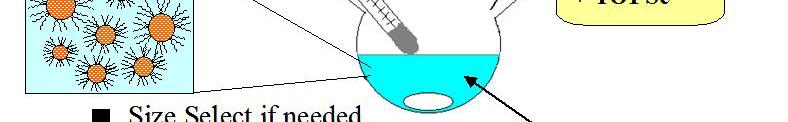
10 Colloidal quantum dots Colloidal synthesis InP QDs synthesized by colloidal methods starting with InCl 3 and tris(trimethylsilyl)phosphine in presence of TOP/TOPO TEM image of 60-Å InP QD (K.Jones, NREL) Small size strong confinement regime small size (15 Å - 80 Å diameter), spherical shape, many confined valence and conduction states [compare to epitaxial SK dots typically > 100 Å, with potential barriers confining ~ 6 conduction and valence states] Variable surface chemistry as-prepared dots are capped with organic stabilizer (TOP/TOPO) surface chemistry alters electrical and optical (emission) properties (pyridine, Na + - biphenyl (-), etched QDs) High ratio of atoms on surface e.g., for 35 Å dots, ~30% of atoms reside on surface importance of surface effects


11 Synthesis of colloidal nanocrystals


12 Synthesis of colloidal nanocrystals Typical three headed flask set up. The middle head is connected to the Schlenk line s glass manifold. The left head is covered with a septum pierced by the thermocouple. The right head is for injection. Photo and caption courtesy of T. Kinner (UT).
.")
 forming a quantum dot lattice that facilitates partial transport (similar to that in a molecular crystal), (2) using")

13 Nanostructures for PV Background Quantum confinement allows more flexibility in electronic structure engineering than the conventional route of alloying bulk materials; but it also results in blocking the carrier transport in the confined dimension(s). Quantum dots could maximize the tunability, but suffer from the shortcoming of being fully confined structures that prevent the carrier transport critically needed for solar cells. A number of approaches have been suggested to restore the carrier transport: (1) forming a quantum dot lattice that facilitates partial transport (similar to that in a molecular crystal), (2) using quasi one dimensional systems (nanowires or nanotubes) as the carrier transporter to extract the photogenerated carriers otherwise trapped in the nanocrystal, (3) using the nanowire or nanotube as absorber, as well as transporter. It is relatively l straightforward ihf using any of these approach to achieve the most basic goal tuning the bandgap but less trivial to also obtain a few other desirable properties specifically for the solar cell. Thus, major effort is required to develop conceptually sound and practical material systems from any of these general approaches.
14 Size dependent optical properties
15 Absorption and emission (CdSe nanocrystals)
16 Size dependent bandgap of CdSe NCs CdSe Murray (1993) & Baskoutas (2006) Meulenberg (2009) Smith (2006) E-gap (ev) Kongkanand (2008) Bulk CdSe bandgap Diameter (nm) From Physical and Optical Properties of Colloidal Semiconducting Nanocrystals for Solar Absorption, by Abdel Ibdah (UT)
17 Colloidal nanostructures (crystalline)
18 Hot electron relaxation pathways Quantum Films vs Quantum Dots phonon bottleneck
19 Electronic Structure Calculations for 41.8 Å InP QD Excitonic energies are calculated using the atomistic pseudopotential ti method (APM). Two steps are involved: 1. single particle orbital energies and wavefunctions are computed by solving the Schrödinger equation; (r R n ) is the screened, nonlocal pseudopotential for the atom of type located at site in cell R n and i is the single particle orbital energy. 1 2 ( r R n ) i 2 Rn i i 2. excitonic energy levels and wavefunctions are calculated using the configuration interaction (CI) approach.
20 Calculated energy levels in 42 Å InP QD (a) Valence States Character of Wavefunction (b) Conduction Character of States Wavefunction State Index Energy (ev) S P D F State Index Energy (ev) S P D F Valence (a) and conduction (b) single particle states for a 41.8 Å diameter InP quantum dot. Columns 3 6 indicate the percentage distribution of envelope angular momentum components for each single particle level Energies are relative to vacuum
21 Calculated excitonic transitions in 42 Å InP QD PEAK POSITION (EV) INITIAL VALENCE STATES , , 4 2, 3, , 8 2, , 3, , 10, 11 14, , 19, 21, 22, 24, FINAL CONDUCTION STATES
22 Excitonic spectrum for 42 Å InP QD Wavelength (nm) Photoindu uced Trans smission (a a.u.) Exc citon Trans ition Intens sity (a.u.) Energy (ev) Theoretical excitonic spectrum (dashed line) for a sample of 41.8 Å diameter InP quantum dots. The transition intensity is proportional to the absorption coefficient, and consists of a sum of the oscillator strengths for various excitonic transitions. The solid line shows the measured photoinduced bleach spectrum, at a delay of 1.0 ps, for a sample with average size of ~42 Å diameter. Theoretical transition peaks correspond to those listed at left. The two small peaks between 2.0 and 2.1 ev originate from transitions between valence states 12, 13, and 15, and conduction state 1.
23 Colloidal PbSe QDs in tetrachloroethylene (TCE) 0.25 Oleic acid-capped PbSe QDs (R = 2.7 nm) in tetrachloroethylene 0.20 E g = 0.76 ev tensity Absorbance (normaliz (O O.D.) zed) = 830 ns minescence Int Photolu Time (s) Wavelength (nm)


24 Silicon Nanocrystals Silicon NC Silicon Nanocrystals (D 9 nm) Absor rbance (O.D.) x Pho otoluminescence e (arb. units) 0.0 L. Mangolini et al. Nano Lett. 5, 655 (2005) Wavelength (nm)


")
 J. E.")
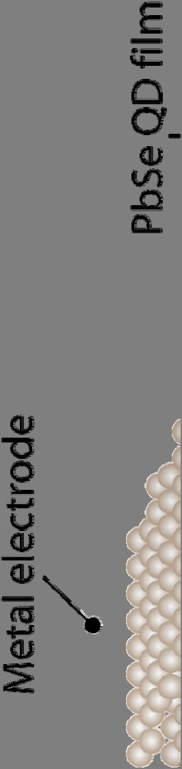
25 Drop cast films of 5.7 nm dia. PbSe NCs oleic acid (1.8 nm) aniline (0.8 nm) ethylenediamine (0.4 nm) J. E. Murphy et al., JACS 128, 3241 (2006).
26 Post casting treatment of spin cast films of PbSe NCs Microstructure of the spin-cast NC films before and after EDT treatment. (a) SAXS data, showing a ~16 Å decrease in the spacing between the NCs and a dramatic loss of superlattice order upon EDT treatment. t t Measurements were taken in air. (b, c) Planview SEM images of (b) an untreated film and (c) a treated film. Scale bars equal one micron. J. Luther, M. Law et al., ACS Nano 2, 271 (2008).
 PbSe NCs in hexane and (2) 0.1 M EDT in anhydrous acetonitrile, allowing the film to dry between each layer. J. M. Luther, M.")
27 Layer by layer fabrication of PbSe NC films EDT = 1,2-ethanedithiol Layer by layer (LbL) fabrication of PbSe nanocrystal (NC) films. Nanocrystal films prepared by dip-coating, alternating between (1) PbSe NCs in hexane and (2) 0.1 M EDT in anhydrous acetonitrile, allowing the film to dry between each layer. J. M. Luther, M. Law et al.,, Structural, Optical, and Electrical Properties of Self-Assembled Films of PbSe Nanocrystals Treated with 1,2-Ethanedithiol, ACS Nano 2, 271 (2008).


28 Novel nanocrystal based solar cell
29 Layer by layer dip coated PbSe films Plan view SEM image of PbSe NC films prepared by layer by layer dip coating onto ITO substrate; scale bar equals 50 nm. The LbL film shown was produced using dip coating cycles cycles. J. Luther, M. Law et al., ACS Nano 2, 271 (2008).


30 Post casting treatment of spin cast films of 7 nm dia. PbSe NCs Characterization: SEM WAXS SAXS FTIR UV Vis IR Absorbance Films spun from octane solution.

31 Annealing NC based films WAXS patterns of a PbSe NC sample at room temperature, t 350, and 500 C in a nitrogen atmosphere. PbSe peaks are labeled with asterisks Law et al., J. AM. CHEM. SOC. 2008, 130,


32 Annealed NC based solar cell Air Stable All Inorganic Nanocrystal Solar Cells Processed from Solution Ilan Gur, Neil A. Fromer, Michael L. Geier, A. Paul Alivisatos 21 OCTOBER 2005 VOL 310 SCIENCE Transmission electron micrographs of (A) CdSe and (B) CdTe NCs used in this investigation. Scale bar, 40 nm. (C) An energy diagram of valence and conduction band levels for CdTe and CdSe illustrates the type II charge transfer junction formed between the two materials


33 Layer by layer dip coated PbSe films Plan view SEM image of PbSe NC films prepared by layer by layer dip coating onto ITO substrate; scale bar equals 50 nm. The LbL film shown was produced using dip coating cycles cycles. J. Luther, M. Law et al., ACS Nano 2, 271 (2008).
Nanostructured Semiconductor Crystals -- Building Blocks for Solar Cells: Shapes, Syntheses, Surface Chemistry, Quantum Confinement Effects
 Nanostructured Semiconductor Crystals -- Building Blocks for Solar Cells: Shapes, Syntheses, Surface Chemistry, Quantum Confinement Effects April 1,2014 The University of Toledo, Department of Physics
Multiple Exciton Generation in Quantum Dots. James Rogers Materials 265 Professor Ram Seshadri
 Multiple Exciton Generation in Quantum Dots James Rogers Materials 265 Professor Ram Seshadri Exciton Generation Single Exciton Generation in Bulk Semiconductors Multiple Exciton Generation in Bulk Semiconductors
Solar Cell Materials and Device Characterization
 Solar Cell Materials and Device Characterization April 3, 2012 The University of Toledo, Department of Physics and Astronomy SSARE, PVIC Principles and Varieties of Solar Energy (PHYS 4400) and Fundamentals
THEORETICAL STUDY OF THE QUANTUM CONFINEMENT EFFECTS ON QUANTUM DOTS USING PARTICLE IN A BOX MODEL
 Journal of Ovonic Research Vol. 14, No. 1, January - February 2018, p. 49-54 THEORETICAL STUDY OF THE QUANTUM CONFINEMENT EFFECTS ON QUANTUM DOTS USING PARTICLE IN A BOX MODEL A. I. ONYIA *, H. I. IKERI,
2004 Debye Lecture 3 C. B. Murray. Semiconductor Nanocrystals Quantum Dots Part 1
 2004 Debye Lecture 3 C. B. Murray Semiconductor Nanocrystals Quantum Dots Part 1 Basic Physics of Semiconductor Quantum Dots C. R. Kagan, IBM T. J. Watson Research Center, Yorktown Heights, NY Conduction
Quantum Dots for Advanced Research and Devices
 Quantum Dots for Advanced Research and Devices spectral region from 450 to 630 nm Zero-D Perovskite Emit light at 520 nm ABOUT QUANTUM SOLUTIONS QUANTUM SOLUTIONS company is an expert in the synthesis
Fabrication / Synthesis Techniques
 Quantum Dots Physical properties Fabrication / Synthesis Techniques Applications Handbook of Nanoscience, Engineering, and Technology Ch.13.3 L. Kouwenhoven and C. Marcus, Physics World, June 1998, p.35
PRESENTED BY: PROF. S. Y. MENSAH F.A.A.S; F.G.A.A.S UNIVERSITY OF CAPE COAST, GHANA.
 SOLAR CELL AND ITS APPLICATION PRESENTED BY: PROF. S. Y. MENSAH F.A.A.S; F.G.A.A.S UNIVERSITY OF CAPE COAST, GHANA. OUTLINE OF THE PRESENTATION Objective of the work. A brief introduction to Solar Cell
More Efficient Solar Cells via Multi Exciton Generation
 More Efficient Solar Cells via Multi Exciton Generation By: MIT Student Instructor: Gang Chen May 14, 2010 1 Introduction Sunlight is the most abundant source of energy available on Earth and if properly
Lecture 6: Individual nanoparticles, nanocrystals and quantum dots
 Lecture 6: Individual nanoparticles, nanocrystals and quantum dots Definition of nanoparticle: Size definition arbitrary More interesting: definition based on change in physical properties. Size smaller
CH676 Physical Chemistry: Principles and Applications. CH676 Physical Chemistry: Principles and Applications
 CH676 Physical Chemistry: Principles and Applications Crystal Structure and Chemistry Synthesis of Tetrahexahedral Platinum Nanocrystals with High-Index Facets and High Electro-Oxidation Activity Na Tian
what happens if we make materials smaller?
 what happens if we make materials smaller? IAP VI/10 ummer chool 2007 Couvin Prof. ns outline Introduction making materials smaller? ynthesis how do you make nanomaterials? Properties why would you make
Quantum Dots The Pennsylvania State University Quantum Dots 1
 Quantum Dots www.nano4me.org 2018 The Pennsylvania State University Quantum Dots 1 Outline Introduction Quantum Confinement QD Synthesis Colloidal Methods Epitaxial Growth Applications Biological Light
Supplementary Materials
 Supplementary Materials Sample characterization The presence of Si-QDs is established by Transmission Electron Microscopy (TEM), by which the average QD diameter of d QD 2.2 ± 0.5 nm has been determined
SUPPLEMENTARY INFORMATION
 SUPPLEMENTARY INFORMATION DOI: 10.1038/NNANO.2012.63 Bright infrared quantum-dot light-emitting diodes through inter-dot spacing control Liangfeng Sun, Joshua J. Choi, David Stachnik, Adam C. Bartnik,
OPTICAL PROPERTIES of Nanomaterials
 OPTICAL PROPERTIES of Nanomaterials Advanced Reading Optical Properties and Spectroscopy of Nanomaterials Jin Zhong Zhang World Scientific, Singapore, 2009. Optical Properties Many of the optical properties
Widely Tunable and Intense Mid-Infrared PL Emission from Epitaxial Pb(Sr)Te Quantum Dots in a CdTe Matrix
Te Quantum Dots in a CdTe Matrix") Widely Tunable and Intense Mid-Infrared PL Emission from Epitaxial Pb(Sr)Te Quantum Dots in a Matrix S. Kriechbaumer 1, T. Schwarzl 1, H. Groiss 1, W. Heiss 1, F. Schäffler 1,T. Wojtowicz 2, K. Koike 3,
Widely Tunable and Intense Mid-Infrared PL Emission from Epitaxial Pb(Sr)Te Quantum Dots in a Matrix S. Kriechbaumer 1, T. Schwarzl 1, H. Groiss 1, W. Heiss 1, F. Schäffler 1,T. Wojtowicz 2, K. Koike 3,
Luminescence basics. Slide # 1
 Luminescence basics Types of luminescence Cathodoluminescence: Luminescence due to recombination of EHPs created by energetic electrons. Example: CL mapping system Photoluminescence: Luminescence due to
Charge Excitation. Lecture 4 9/20/2011 MIT Fundamentals of Photovoltaics 2.626/2.627 Fall 2011 Prof. Tonio Buonassisi
 Charge Excitation Lecture 4 9/20/2011 MIT Fundamentals of Photovoltaics 2.626/2.627 Fall 2011 Prof. Tonio Buonassisi 1 2.626/2.627 Roadmap You Are Here 2 2.626/2.627: Fundamentals Every photovoltaic device
SYNTHESIS OF CADMIUM SULFIDE NANOSTRUCTURES BY NOVEL PRECURSOR
 Nanomaterials: Applications and Properties (NAP-2011). Vol. 1, Part I 107 SYNTHESIS OF CADMIUM SULFIDE NANOSTRUCTURES BY NOVEL PRECURSOR M. Salavati Niasari 1,2* 1 Department of Inorganic Chemistry, Faculty
Semiconductor quantum dots
 Semiconductor quantum dots Quantum dots are spherical nanocrystals of semiconducting materials constituted from a few hundreds to a few thousands atoms, characterized by the quantum confinement of the
CHAPTER 3. OPTICAL STUDIES ON SnS NANOPARTICLES
 42 CHAPTER 3 OPTICAL STUDIES ON SnS NANOPARTICLES 3.1 INTRODUCTION In recent years, considerable interest has been shown on semiconducting nanostructures owing to their enhanced optical and electrical
Role of Surface Chemistry on Charge Carrier Transport in Quantum Dot Solids
 Role of Surface Chemistry on Charge Carrier Transport in Quantum Dot Solids Cherie R. Kagan, University of Pennsylvania in collaboration with the Murray group Density of Electronic States in Quantum Dot
Starting solution. Hydrolysis reaction under thermostatic conditions. Check of viscosity and deposition test SOL. Deposition by spin coating
 Supplementary Figures Tetramethyl orthosilicate (TMOS) Tetrahydrofuran anhydrous (THF) Trimethyl methoxy silane (TMMS) Trimethyl silil acetate (TMSA) Starting solution Hydrolysis reaction under thermostatic
Q. Shen 1,2) and T. Toyoda 1,2)
 and T. Toyoda 1,2)") Photosensitization of nanostructured TiO 2 electrodes with CdSe quntum dots: effects of microstructure in substrates Q. Shen 1,2) and T. Toyoda 1,2) Department of Applied Physics and Chemistry 1), and
Photosensitization of nanostructured TiO 2 electrodes with CdSe quntum dots: effects of microstructure in substrates Q. Shen 1,2) and T. Toyoda 1,2) Department of Applied Physics and Chemistry 1), and
Organic LEDs part 8. Exciton Dynamics in Disordered Organic Thin Films. Handout on QD-LEDs: Coe et al., Nature 420, 800 (2002).
.") Organic LEDs part 8 Exciton Dynamics in Disordered Organic Thin Films Quantum Dot LEDs Handout on QD-LEDs: Coe et al., ature 420, 800 (2002). @ MIT April 29, 2003 Organic Optoelectronics - Lecture 20b
Organic LEDs part 8 Exciton Dynamics in Disordered Organic Thin Films Quantum Dot LEDs Handout on QD-LEDs: Coe et al., ature 420, 800 (2002). @ MIT April 29, 2003 Organic Optoelectronics - Lecture 20b
Three-Dimensional Silicon-Germanium Nanostructures for Light Emitters and On-Chip Optical. Interconnects
 Three-Dimensional Silicon-Germanium Nanostructures for Light Emitters and On-Chip Optical eptember 2011 Interconnects Leonid Tsybeskov Department of Electrical and Computer Engineering New Jersey Institute
Intensity / a.u. 2 theta / deg. MAPbI 3. 1:1 MaPbI 3-x. Cl x 3:1. Supplementary figures
 Intensity / a.u. Supplementary figures 110 MAPbI 3 1:1 MaPbI 3-x Cl x 3:1 220 330 0 10 15 20 25 30 35 40 45 2 theta / deg Supplementary Fig. 1 X-ray Diffraction (XRD) patterns of MAPbI3 and MAPbI 3-x Cl
Multiple exciton generation in semiconductor nanocrystals: Toward efficient solar energy conversion
 Early View publication on www.interscience.wiley.com (issue and page numbers not yet assigned; citable using Digital Object Identifier DOI) Laser & Photon. Rev., 1 23 (2008) / DOI 10.1002/lpor.200810013
Chapter 3 Properties of Nanostructures
 Chapter 3 Properties of Nanostructures In Chapter 2, the reduction of the extent of a solid in one or more dimensions was shown to lead to a dramatic alteration of the overall behavior of the solids. Generally,
OPTICAL PROPERTIES AND SPECTROSCOPY OF NANOAAATERIALS. Jin Zhong Zhang. World Scientific TECHNISCHE INFORMATIONSBIBLIOTHEK
 OPTICAL PROPERTIES AND SPECTROSCOPY OF NANOAAATERIALS Jin Zhong Zhang University of California, Santa Cruz, USA TECHNISCHE INFORMATIONSBIBLIOTHEK Y World Scientific NEW JERSEY. t'on.don SINGAPORE «'BEIJING
Development of active inks for organic photovoltaics: state-of-the-art and perspectives
 Development of active inks for organic photovoltaics: state-of-the-art and perspectives Jörg Ackermann Centre Interdisciplinaire de Nanoscience de Marseille (CINAM) CNRS - UPR 3118, MARSEILLE - France
1. Depleted heterojunction solar cells. 2. Deposition of semiconductor layers with solution process. June 7, Yonghui Lee
 1. Depleted heterojunction solar cells 2. Deposition of semiconductor layers with solution process June 7, 2016 Yonghui Lee Outline 1. Solar cells - P-N junction solar cell - Schottky barrier solar cell
Nanomaterials for Photovoltaics (v11) 14. Intermediate-Band Solar Cells
 14. Intermediate-Band Solar Cells") 1 14. Intermediate-Band Solar Cells Intermediate (impurity) band solar cells (IBSCs) (I) Concept first proposed by A. Luque and A. Martí in 1997. Establish an additional electronic band within the band
1 14. Intermediate-Band Solar Cells Intermediate (impurity) band solar cells (IBSCs) (I) Concept first proposed by A. Luque and A. Martí in 1997. Establish an additional electronic band within the band
Self-Assembled InAs Quantum Dots
 Self-Assembled InAs Quantum Dots Steve Lyon Department of Electrical Engineering What are semiconductors What are semiconductor quantum dots How do we make (grow) InAs dots What are some of the properties
Quantum Dot Spectrum Converter Coverglass for Enhanced High Efficiency Photovoltaics
 Quantum Dot Spectrum Converter Coverglass for Enhanced High Efficiency Photovoltaics Theodore G. Stern DR Technologies, Inc. San Diego, CA 92020 Business Area Manager Space Power, Optical and Thermal Products
Materials as particle in a box models: Synthesis & optical study of CdSe quantum dots
 Lab Week 3 Module α 2 Materials as particle in a box models: Synthesis & optical study of CdSe quantum dots Instructor: Francesco Stellacci OBJECTIVES Introduce the particle-wave duality principle Introduce
Quantum confined nanocrystals and nanostructures for high efficiency solar photoconversion Matthew C. Beard
 Quantum confined nanocrystals and nanostructures for high efficiency solar photoconversion Matthew C. Beard NREL is a national laboratory of the U.S. Department of Energy, Office of Energy Efficiency and
Forming Gradient Multilayer (GML) Nano Films for Photovoltaic and Energy Storage Applications
 Nano Films for Photovoltaic and Energy Storage Applications") Forming Gradient Multilayer (GML) Nano Films for Photovoltaic and Energy Storage Applications ABSTRACT Boris Gilman and Igor Altman Coolsol R&C, Mountain View CA For successful implementation of the nanomaterial-based
Forming Gradient Multilayer (GML) Nano Films for Photovoltaic and Energy Storage Applications ABSTRACT Boris Gilman and Igor Altman Coolsol R&C, Mountain View CA For successful implementation of the nanomaterial-based
Solar Cells Based on. Quantum Dots: Multiple Exciton Generation and Intermediate Bands Antonio Luque, Antonio Marti, and Arthur J.
 Solar Cells Based on Quantum Dots: Multiple Exciton Generation and Intermediate Bands Antonio Luque, Antonio Marti, and Arthur J. Nozik Student ID: 2004171039 Name: Yo-Han Choi Abstract Semiconductor quantum
Title: Colloidal Quantum Dots Intraband Photodetectors
 Title: Colloidal Quantum Dots Intraband Photodetectors Authors: Zhiyou Deng, Kwang Seob Jeong, and Philippe Guyot-Sionnest* Supporting Information: I. Considerations on the optimal detectivity of interband
Optics and Quantum Optics with Semiconductor Nanostructures. Overview
 Optics and Quantum Optics with Semiconductor Nanostructures Stephan W. Koch Department of Physics, Philipps University, Marburg/Germany and Optical Sciences Center, University of Arizona, Tucson/AZ Overview
A. OTHER JUNCTIONS B. SEMICONDUCTOR HETEROJUNCTIONS -- MOLECULES AT INTERFACES: ORGANIC PHOTOVOLTAIC BULK HETEROJUNCTION DYE-SENSITIZED SOLAR CELL
 A. OTHER JUNCTIONS B. SEMICONDUCTOR HETEROJUNCTIONS -- MOLECULES AT INTERFACES: ORGANIC PHOTOVOLTAIC BULK HETEROJUNCTION DYE-SENSITIZED SOLAR CELL March 24, 2015 The University of Toledo, Department of
A. OTHER JUNCTIONS B. SEMICONDUCTOR HETEROJUNCTIONS -- MOLECULES AT INTERFACES: ORGANIC PHOTOVOLTAIC BULK HETEROJUNCTION DYE-SENSITIZED SOLAR CELL
 A. OTHER JUNCTIONS B. SEMICONDUCTOR HETEROJUNCTIONS -- MOLECULES AT INTERFACES: ORGANIC PHOTOVOLTAIC BULK HETEROJUNCTION DYE-SENSITIZED SOLAR CELL February 9 and 14, 2012 The University of Toledo, Department
ULTRAFAST SPECTROSCOPY OF CHEMICALLY SYNTHESIZED SEMICONDUCTOR NANOPARTICLES
 Summerschool on SEMICONDUCTOR QUANTUM DOTS: PHYSICS AND DEVICES Monte Verità, Ascona, Switzerland Sunday September 5, to Friday September 10, 2004 ULTRAFAST SPECTROSCOPY OF CHEMICALLY SYNTHESIZED SEMICONDUCTOR
Novel materials and nanostructures for advanced optoelectronics
 Novel materials and nanostructures for advanced optoelectronics Q. Zhuang, P. Carrington, M. Hayne, A Krier Physics Department, Lancaster University, UK u Brief introduction to Outline Lancaster University
Prediction of a Shape-Induced Enhancement in the Hole Relaxation in Nanocrystals
 Prediction of a Shape-Induced Enhancement in the Hole Relaxation in Nanocrystals NANO LETTERS 2003 Vol. 3, No. 9 1197-1202 Marco Califano,* Gabriel Bester, and Alex Zunger National Renewable Energy Laboratory,
Photocatalysis: semiconductor physics
 Photocatalysis: semiconductor physics Carlos J. Tavares Center of Physics, University of Minho, Portugal ctavares@fisica.uminho.pt www.fisica.uminho.pt 1 Guimarães Where do I come from? 3 Guimarães 4 Introduction>>
interband transitions in semiconductors M. Fox, Optical Properties of Solids, Oxford Master Series in Condensed Matter Physics
 interband transitions in semiconductors M. Fox, Optical Properties of Solids, Oxford Master Series in Condensed Matter Physics interband transitions in quantum wells Atomic wavefunction of carriers in
Luminescence Process
 Luminescence Process The absorption and the emission are related to each other and they are described by two terms which are complex conjugate of each other in the interaction Hamiltonian (H er ). In an
Variation of Electronic State of CUBOID Quantum Dot with Size
 Nano Vision, Vol.1 (1), 25-33 (211) Variation of Electronic State of CUBOID Quantum Dot with Size RAMA SHANKER YADAV and B. S. BHADORIA* Department of Physics, Bundelkhand University, Jhansi-284128 U.P.
Electroluminescence from Silicon and Germanium Nanostructures
 Electroluminescence from silicon Silicon Getnet M. and Ghoshal S.K 35 ORIGINAL ARTICLE Electroluminescence from Silicon and Germanium Nanostructures Getnet Melese* and Ghoshal S. K.** Abstract Silicon
Nanoelectronics. Topics
 Nanoelectronics Topics Moore s Law Inorganic nanoelectronic devices Resonant tunneling Quantum dots Single electron transistors Motivation for molecular electronics The review article Overview of Nanoelectronic
Fabrication of Core/Shell. structured Nanoparticles
 Fabrication of Core/Shell structured Nanoparticles Core + Shell Representative heterogeneous nucleation Peter Reiss,* Myriam Protie`re, and Liang Li, Core/Shell Semiconductor Nanocrystals, Small 2009,
1 Semiconductor Quantum Dots for Ultrafast Optoelectronics
 j1 1 Semiconductor Quantum Dots for Ultrafast Optoelectronics 1.1 The Role of Dimensionality in Semiconductor Materials The history of semiconductor lasers has been punctuated by dramatic revolutions.
Challenges in to-electric Energy Conversion: an Introduction
 Challenges in Solar-to to-electric Energy Conversion: an Introduction Eray S. Aydil Chemical Engineering and Materials Science Department Acknowledgements: National Science Foundation Minnesota Initiative
Defense Technical Information Center Compilation Part Notice
 UNCLASSIFIED Defense Technical Information Center Compilation Part Notice ADP013097 TITLE: Optically Detected Magnetic Resonance of Semiconductor Quantum Dots DISTRIBUTION: Approved for public release,
Introduction to semiconductor nanostructures. Peter Kratzer Modern Concepts in Theoretical Physics: Part II Lecture Notes
 Introduction to semiconductor nanostructures Peter Kratzer Modern Concepts in Theoretical Physics: Part II Lecture Notes What is a semiconductor? The Fermi level (chemical potential of the electrons) falls
Semiconductor Quantum Structures And Energy Conversion. Itaru Kamiya Toyota Technological Institute
 Semiconductor Quantum Structures And nergy Conversion April 011, TTI&NCHU Graduate, Special Lectures Itaru Kamiya kamiya@toyota-ti.ac.jp Toyota Technological Institute Outline 1. Introduction. Principle
Transition from Molecular Vibrations to Phonons in Atomically Precise Cadmium Selenide Quantum Dots
 Supporting Information for Transition from Molecular Vibrations to Phonons in Atomically Precise Cadmium Selenide Quantum Dots Alexander N. Beecher, Rachel A. Dziatko, Michael L. Steigerwald, Jonathan
GeSi Quantum Dot Superlattices
 GeSi Quantum Dot Superlattices ECE440 Nanoelectronics Zheng Yang Department of Electrical & Computer Engineering University of Illinois at Chicago Nanostructures & Dimensionality Bulk Quantum Walls Quantum
Optoelectronics and. Colloidal Quantum Dot. Photovoltaics. Cambridge GERASIMOS KONSTANTATOS EDWARD H. SARGENT. University of Toronto.
 Colloidal Quantum Dot Optoelectronics and Photovoltaics Edited by GERASIMOS KONSTANTATOS ICFO The Institute of Photonic Sciences, Barcelona EDWARD H. SARGENT University of Toronto Cambridge UNIVERSITY
Quantum Dot Technology for Low-Cost Space Power Generation for Smallsats
 SSC06-VI- Quantum Dot Technology for Low-Cost Space Power Generation for Smallsats Theodore G. DR Technologies, Inc. 7740 Kenamar Court, San Diego, CA 92020 (858)677-230 tstern@drtechnologies.com The provision
Optical Science of Nano-graphene (graphene oxide and graphene quantum dot) Introduction of optical properties of nano-carbon materials
 Introduction of optical properties of nano-carbon materials") Optical Science of Nano-graphene (graphene oxide and graphene quantum dot) J Kazunari Matsuda Institute of Advanced Energy, Kyoto University Introduction of optical properties of nano-carbon materials
Optical Science of Nano-graphene (graphene oxide and graphene quantum dot) J Kazunari Matsuda Institute of Advanced Energy, Kyoto University Introduction of optical properties of nano-carbon materials
Supporting Information for: Heavy-Metal-Free Fluorescent ZnTe/ZnSe Nanodumbbells
 Supporting Information for: Heavy-Metal-Free Fluorescent ZnTe/ZnSe Nanodumbbells Botao Ji, Yossef E. Panfil and Uri Banin * The Institute of Chemistry and Center for Nanoscience and Nanotechnology, The
QUANTUM WELLS, WIRES AND DOTS
 QUANTUM WELLS, WIRES AND DOTS Theoretical and Computational Physics of Semiconductor Nanostructures Second Edition Paul Harrison The University of Leeds, UK /Cf}\WILEY~ ^INTERSCIENCE JOHN WILEY & SONS,
DOI: /jacs.7b02953 J. Am. Chem. Soc. 2017, 139,
 DOI: 10.1021/jacs.7b02953 J. Am. Chem. Soc. 2017, 139, 6761 6770 Manju C K 01.07.2017 Introduction In the last several decades, colloidal chemistry has provided effective ways to synthesize inorganic nanomaterials
Temperature Dependent Optical Band Gap Measurements of III-V films by Low Temperature Photoluminescence Spectroscopy
 Temperature Dependent Optical Band Gap Measurements of III-V films by Low Temperature Photoluminescence Spectroscopy Linda M. Casson, Francis Ndi and Eric Teboul HORIBA Scientific, 3880 Park Avenue, Edison,
AN ELABORATION OF QUANTUM DOTS AND ITS APPLICATIONS
 AN ELABORATION OF QUANTUM DOTS AND ITS APPLICATIONS Sambeet Mishra 1, Bhagabat Panda 2, Suman Saurav Rout 3 1,3 School of Electrical Engineering, KIIT University, Bhubaneswar, India 2 Asst. Professor,
Nanoscience galore: hybrid and nanoscale photonics
 Nanoscience galore: hybrid and nanoscale photonics Pavlos Lagoudakis SOLAB, 11 June 2013 Hybrid nanophotonics Nanostructures: light harvesting and light emitting devices 2 Hybrid nanophotonics Nanostructures:
A. OTHER JUNCTIONS B. SEMICONDUCTOR HETEROJUNCTIONS -- MOLECULES AT INTERFACES: ORGANIC PHOTOVOLTAIC BULK HETEROJUNCTION DYE-SENSITIZED SOLAR CELL
 A. OTHER JUNCTIONS B. SEMICONDUCTOR HETEROJUNCTIONS -- MOLECULES AT INTERFACES: ORGANIC PHOTOVOLTAIC BULK HETEROJUNCTION DYE-SENSITIZED SOLAR CELL March 20, 2014 The University of Toledo, Department of
Graphene and Carbon Nanotubes
 Graphene and Carbon Nanotubes 1 atom thick films of graphite atomic chicken wire Novoselov et al - Science 306, 666 (004) 100μm Geim s group at Manchester Novoselov et al - Nature 438, 197 (005) Kim-Stormer
III-V nanostructured materials synthesized by MBE droplet epitaxy
 III-V nanostructured materials synthesized by MBE droplet epitaxy E.A. Anyebe 1, C. C. Yu 1, Q. Zhuang 1,*, B. Robinson 1, O Kolosov 1, V. Fal ko 1, R. Young 1, M Hayne 1, A. Sanchez 2, D. Hynes 2, and
Morphology of CdSe/ZnS core/shell QDs coated on textured surface with SiN X film of a
 Electronic Supplementary Material (ESI) for Nanoscale. This journal is The Royal Society of Chemistry 2014 Supplementary/supporting information Morphology of CdSe/ZnS core/shell QDs coated on textured
Bright CuInS 2 /CdS Nanocrystal Phosphors for High-Gain Full-Spectrum Luminescent Solar Concentrators
 Electronic Supplementary Material (ESI) for ChemComm. This journal is The Royal Society of Chemistry 215 Knowles et al. March 8, 215 Supplementary Information Bright Nanocrystal Phosphors for High-Gain
Optical spectroscopy of carrier dynamics in semiconductor nanostructures de Jong, E.M.L.D.
 UvA-DARE (Digital Academic Repository) Optical spectroscopy of carrier dynamics in semiconductor nanostructures de Jong, E.M.L.D. Link to publication Citation for published version (APA): de Jong, EM-LD.
not to be confused with using the materials to template nanostructures
 Zeolites as Templates: continued Synthesis: Most zeolite syntheses are performed by using template-synthesis not to be confused with using the materials to template nanostructures templates are often surfactants
Scienza e Tecnologia dei Materiali Ceramici. Modulo 2: Materiali Nanostrutturati
 Università degli Studi di Trieste Dipartimento di Ingegneria e Architettura A.A. 2016-2017 Scienza e Tecnologia dei Materiali Ceramici Modulo 2: Materiali Nanostrutturati - Lezione 5 - Vanni Lughi vlughi@units.it
Tianle Guo, 1 Siddharth Sampat, 1 Kehao Zhang, 2 Joshua A. Robinson, 2 Sara M. Rupich, 3 Yves J. Chabal, 3 Yuri N. Gartstein, 1 and Anton V.
 SUPPLEMENTARY INFORMATION for Order of magnitude enhancement of monolayer MoS photoluminescence due to near-field energy influx from nanocrystal films Tianle Guo, Siddharth Sampat, Kehao Zhang, Joshua
Conductivity and Semi-Conductors
 Conductivity and Semi-Conductors J = current density = I/A E = Electric field intensity = V/l where l is the distance between two points Metals: Semiconductors: Many Polymers and Glasses 1 Electrical Conduction
Mesoporous titanium dioxide electrolyte bulk heterojunction
 Mesoporous titanium dioxide electrolyte bulk heterojunction The term "bulk heterojunction" is used to describe a heterojunction composed of two different materials acting as electron- and a hole- transporters,
Supplementary Figure S1 TEM images of a synthesis batch of PbS and Bi-doped PbS QDs (Bi/Pb=3.2%) and corresponding size distribution histograms (100
 and corresponding size distribution histograms (100") Supplementary Figure S1 TEM images of a synthesis batch of PbS and Bi-doped PbS QDs (Bi/Pb=3.2%) and corresponding size distribution histograms (100 QDs population in each sample) yielding average diameters
Supplementary Figure S1 TEM images of a synthesis batch of PbS and Bi-doped PbS QDs (Bi/Pb=3.2%) and corresponding size distribution histograms (100 QDs population in each sample) yielding average diameters
CHAPTER III. ORGANIC LIGANDS PASSIVATED ZnSe NANOSTRUCTURES AND FUNCTIONAL PROPERTIES
 82 CHAPTER III ORGANIC LIGANDS PASSIVATED ZnSe NANOSTRUCTURES AND FUNCTIONAL PROPERTIES 3.1 INTRODUCTION Semiconductor nanocrystals have size tunable optical properties that open up possibilities for revolutionary
Supplementary Figure S1. The maximum possible short circuit current (J sc ) from a solar cell versus the absorber band-gap calculated assuming 100%
 from a solar cell versus the absorber band-gap calculated assuming 100%") Supplementary Figure S1. The maximum possible short circuit current (J sc ) from a solar cell versus the absorber band-gap calculated assuming 100% (black) and 80% (red) external quantum efficiency (EQE)
Supplementary Figure S1. The maximum possible short circuit current (J sc ) from a solar cell versus the absorber band-gap calculated assuming 100% (black) and 80% (red) external quantum efficiency (EQE)
Spectroscopy at nanometer scale
 Spectroscopy at nanometer scale 1. Physics of the spectroscopies 2. Spectroscopies for the bulk materials 3. Experimental setups for the spectroscopies 4. Physics and Chemistry of nanomaterials Various
Seminars in Nanosystems - I
 Seminars in Nanosystems - I Winter Semester 2011/2012 Dr. Emanuela Margapoti Emanuela.Margapoti@wsi.tum.de Dr. Gregor Koblmüller Gregor.Koblmueller@wsi.tum.de Seminar Room at ZNN 1 floor Topics of the
Optical properties of nano-silicon
 Bull. Mater. Sci., Vol. 4, No. 3, June 001, pp. 85 89. Indian Academy of Sciences. Optical properties of nano-silicon S TRIPATHY, R K SONI*, S K GHOSHAL and K P JAIN Department of Physics, Indian Institute
CHAPTER IV SYNTHESIS AND CHARACTERIZATION OF METAL IONS DOPED ZINC SELENIDE NANOPARTICLES
 132 CHAPTER IV SYNTHESIS AND CHARACTERIZATION OF METAL IONS DOPED ZINC SELENIDE NANOPARTICLES 4.1 Introduction Introducing impurity atoms into a semiconductor host leads to an increase in the free-carrier
Supplementary Figure 1 XRD pattern of a defective TiO 2 thin film deposited on an FTO/glass substrate, along with an XRD pattern of bare FTO/glass
 Supplementary Figure 1 XRD pattern of a defective TiO 2 thin film deposited on an FTO/glass substrate, along with an XRD pattern of bare FTO/glass and a reference pattern of anatase TiO 2 (JSPDS No.: 21-1272).
University of Louisville - Department of Chemistry, Louisville, KY; 2. University of Louisville Conn Center for renewable energy, Louisville, KY; 3
 Ultrafast transient absorption spectroscopy investigations of charge carrier dynamics of methyl ammonium lead bromide (CH 3 NH 3 PbBr 3 ) perovskite nanostructures Hamzeh Telfah 1 ; Abdelqader Jamhawi
STRUCTURAL, OPTICAL AND ELECTRICAL CHARACTERIZATION OF CdSe NANOPARTICLES
 Chalcogenide Letters Vol. 6, No. 9, September 2009, p. 477 482 STRUCTURAL, OPTICAL AND ELECTRICAL CHARACTERIZATION OF CdSe NANOPARTICLES A. MANNA, R. BHATTACHARYA, S. SAHA * Department of Physics and Technophysics,
Transparent TiO 2 nanotube/nanowire arrays on TCO coated glass substrates: Synthesis and application to solar energy conversion
 Transparent TiO 2 nanotube/nanowire arrays on TCO coated glass substrates: Synthesis and application to solar energy conversion Craig A. Grimes Department of Electrical Engineering Center for Solar Nanomaterials
Metal Vapour Lasers Use vapoured metal as a gain medium Developed by W. Silfvast (1966) Two types: Ionized Metal vapour (He-Cd) Neutral Metal vapour
 Two types: Ionized Metal vapour (He-Cd) Neutral Metal vapour") Metal Vapour Lasers Use vapoured metal as a gain medium Developed by W. Silfvast (1966) Two types: Ionized Metal vapour (He-Cd) Neutral Metal vapour (Cu) All operate by vaporizing metal in container Helium
Metal Vapour Lasers Use vapoured metal as a gain medium Developed by W. Silfvast (1966) Two types: Ionized Metal vapour (He-Cd) Neutral Metal vapour (Cu) All operate by vaporizing metal in container Helium
SYNTHESIS AND PARTICLE SIZE CHARACTERIZATION OF CdSe SEMICONDUCTOR QUANTUM DOTS
 International Journal of Metallurgical & Materials Science and Engineering (IJMMSE) ISSN(P): 2278-2516; ISSN(E): 2278-2524 Vol. 3, Issue 5, Dec 2013, 37-46 TJPRC Pvt. Ltd. SYNTHESIS AND PARTICLE SIZE CHARACTERIZATION
The Use of Quantum Dots for Solar Energy Conversion: A Brief Review
 JUST, Vol. IV, No. 1, 2016 Trent University The Use of Quantum Dots for Solar Energy Conversion: A Brief Review Hamza Khattak Abstract One of the more rapidly growing fields in science today is solar energy
Supporting Information
 Electronic Supplementary Material (ESI) for ChemComm. This journal is The Royal Society of Chemistry 2015 Supporting Information All inorganic cesium lead halide perovskite nanocrystals for photodetector
Impact Ionization Can Explain Carrier Multiplication in PbSe Quantum Dots
 Impact Ionization Can Explain Carrier Multiplication in PbSe Quantum Dots A. Franceschetti,* J. M. An, and A. Zunger National Renewable Energy Laboratory, Golden, Colorado 8040 Received May 3, 2006; Revised
Part I. Nanostructure design and structural properties of epitaxially grown quantum dots and nanowires
 Part I Nanostructure design and structural properties of epitaxially grown quantum dots and nanowires 1 Growth of III V semiconductor quantum dots C. Schneider, S. Höfling and A. Forchel 1.1 Introduction
Physics and Material Science of Semiconductor Nanostructures
 Physics and Material Science of Semiconductor Nanostructures PHYS 570P Prof. Oana Malis Email: omalis@purdue.edu Course website: http://www.physics.purdue.edu/academic_programs/courses/phys570p/ 1 Course
Size-Dependent Biexciton Quantum Yields and Carrier Dynamics of Quasi-
 Supporting Information Size-Dependent Biexciton Quantum Yields and Carrier Dynamics of Quasi- Two-Dimensional Core/Shell Nanoplatelets Xuedan Ma, Benjamin T. Diroll, Wooje Cho, Igor Fedin, Richard D. Schaller,