Role of Surface Chemistry on Charge Carrier Transport in Quantum Dot Solids
|
|
|
- Cassandra Hood
- 6 years ago
- Views:
Transcription


1 Role of Surface Chemistry on Charge Carrier Transport in Quantum Dot Solids Cherie R. Kagan, University of Pennsylvania in collaboration with the Murray group
2 Density of Electronic States in Quantum Dot Solids ligand exchange E o Energy E o E o doping chemically electrochemically electrostatically photo-carrier recombination carrier transport E o Density of States Kagan, Murray, Nat. Nano 10, 1013 (2015)


3 Examples of Ligand Exchange in Pb-Chalcogenide Quantum Dot Solids BDT NH 4 Cl SCN OA EDT TBAB organic inorganic SCN+PbCl 2 MPA TBAI


4 Field-Effect Transistor Measurements V D + metalsemiconductor Energy - Density of States semiconductorgate dielectric n or p ( V V ) G q T C OX metal-semiconductor and semiconductor-gate oxide interfaces affect measurements induced carrier concentration depends on the gate voltage shifting the quasi-fermi level

![current I D [A] 10-5 10-6 10-7 10-8 EDT V DS =50V Al Ag Pd Cr Au -50-25 0 25 50 I](/docs-images/80/80605899/images/5-1.jpg "D [A] 10-3 10-4 10-5 10-6 Al Ag Pd Cr Au V DS SCN =50V -50-25 0 25 50 I D [A]")

5 Charge Injection and Transport in PbSe Quantum Dot FETs workfunction electron affinity charge injection and transport control the polarity and magnitude of the current I D [A] EDT V DS =50V Al Ag Pd Cr Au I D [A] Al Ag Pd Cr Au V DS SCN =50V I D [A] TBAI V DS =50V coupling ligand Oh, Wang, Berry, Choi, Zhao, Gaulding, Paik, Lai, Murray, Kagan, Nano Lett 14, 6210 (2014).

![3 Å -40-30 -20-10 0 10 20 30 40 C max 2 Å 1.2 Å 0.9 Å 0.6 Å Capacitance [nf] 0.68 0.67 0.66 0.65 0.64 0.63 0.62 0.61 0.60 Se deposition 1.2 Å 0.9 0.6 Å 0.](/docs-images/80/80605899/images/6-3.jpg "3 Å 0 Å Se rich p-type device -40-30 -20-10 0 10 20 30 40 C max controlled carrier concentration over the range of 10 15 /cm 3-10 20 /cm 3 Oh, Berry, Choi, Gaulding, Paik, Hong,")
6 Stoichiometric Control of Pb-Chalcogenide Thin-Film QD Solids NH 4 SCN RT substrate Excess Pb deposition CB Pb rich n-type device E Ei VB PbX NCs device Excess Se deposition N Pb or N Se U. SCHLICHTING and K. H. GOBRECHT, J. Phys, Chem. Solids, 1973, 34, 753 Capacitance [nf] Pb deposition 0 Å 0.3 Å C max 2 Å 1.2 Å 0.9 Å 0.6 Å Capacitance [nf] Se deposition 1.2 Å Å 0.3 Å 0 Å Se rich p-type device C max controlled carrier concentration over the range of /cm /cm 3 Oh, Berry, Choi, Gaulding, Paik, Hong, Murray, Kagan, ACS Nano 7, 2413 (2013)

![Pb 0.1 Å Se I D [A] 10-4 10-5 10-6 Excess Pb pristine 1A 2A 3A 4A I D](/docs-images/80/80605899/images/7-1.jpg "[A] 10-7 -60-40 -20 0 20 40 60 Excess Se 10-5 10-6 pristine 0.3A 0.")

7 Case Study: Stoichiometric Control of Carrier Statistics in Pbchalcogenide Quantum Dot Thin Films I D [A] V DS =50V 1 Å Pb 0.1 Å Se I D [A] Excess Pb pristine 1A 2A 3A 4A I D [A] Excess Se pristine 0.3A 0.1A 0.4A 0.2A 0.5A V DS =-50V V DS =50V Pb Se At 2-3 Å Pb, µ e ~10 cm 2 /Vs At Å Se, µ h ~0.5 cm 2 /Vs


")


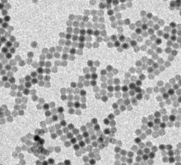
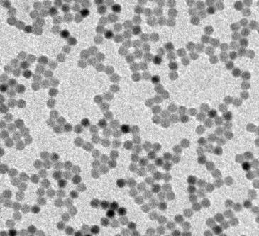
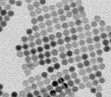
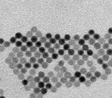
8 Solution-based Stoichiometric Control of PbE (E=S, Se) Quantum Dot Thin Films Insulating Film P-type Device Na2Se (Na2S, KHS) N-type Device PbCl nm 10nm 10nm hexagonal to square ordered assemblies driven by high chalcogen surface energy akin to ligand stripping by Vanmaekelbergh, Hanrath.. Oh, Berry, Choi, Gaulding, Lin, Paik, Diroll, Muramoto, Murray, Kagan, Nano Lett 14, 1559 (2013).
9 As-synthesized NCs Stoichiometry Change Chalcogen-rich NCs Lead-rich NCs Na 2 Se (Na 2 S, KHS) PbCl 2 No. of Pb atoms : 2190 No. of Se atoms :1925 = < +620 No. of Pb atoms : 2190 No. of Se atoms : < = No. of Pb atoms : 2754 No. of Se atoms : 2558 Pb:Se (model)=1.137:1 Pb:Se (model)=0.847:1 Pb:Se (model)=1.065:1 Pb:Se (by ICP)=1.145:1 Pb:Se (by ICP)=0.841:1 Pb:Se (by ICP)=1.073:1

10 Flash-Photolysis, Time-Resolved Microwave Conductivity Energy Gτ n Gτ p generation rate, G Density of States Δn,p = Gτ n,p 0 at low intensity contactless Fermi energy unaltered by measurement, particularly at low intensity time-resolution limited by cavity response and microwave frequency in the ns-µs Goodwin, Straus, Gaulding, Murray, Kagan, Chemical Physics, (2016)
 10-6 10-7")

11 TRMC Measurements of Doped PbSe Quantum Dot Thin Films I D (A) (V) carrier mobility increases as Fermi level approaches the band edges
 Goodwin, Diroll, Oh, Paik, Murray, Kagan, J. Phys.")
12 Quantum Dot Surface Repair in IV-VI Materials solvents and ligand exchange processes strip atoms from the quantum dot surface Owen, Hens, Sargent, Pb:Se ratio OA SCN SCN+PbCl 2 Oh, Wang, Berry, Choi, Zhao, Gaulding, Paik, Lai, Murray, Kagan, Nano Lett 14, 6210 (2014) Goodwin, Diroll, Oh, Paik, Murray, Kagan, J. Phys. Chem C 118, (2014).

![0 20 40 60 I D [A] 10-3 10-4 10-5 10-6 V DS =50V -60-40 -20 0 20 40 60 doping PbCl](/docs-images/80/80605899/images/13-1.jpg "2 as electron concentration increases through chemical or electrostatic doping or")

13 Coupling and Carrier Concentration Dependent Transport in PbSe Quantum Dot FETs Al Au Energy Density of States I D [A] V DS =-50V I D [A] V DS =50V doping PbCl 2 as electron concentration increases through chemical or electrostatic doping or charge injection, transport transitions from hopping to more extended state σ [S/cm] SCN - + PbCl 2 SCN - EDT MPA T [K] I -


14 Integrated Quantum Dot CMOS Inverter V DD =-50V 12 V OUT V IN V OUT 8 4 Gain V IN 0

![Current density [ma/cm 2 ] 20 10 0-10](/docs-images/80/80605899/images/15-1.jpg "PCE: 0 % PCE: 1.3% PCE: 2.2% -20-0.")


![SCN/ BDT 10 0 10-1 10-2 Lifetime [µs]](/docs-images/80/80605899/images/15-5.jpg "Oh, Straus, Zhao, Choi, Lee,")
15 Can Solar Cells Be Fabricated from Strongly-Coupled NCs? Current density [ma/cm 2 ] PCE: 0 % PCE: 1.3% PCE: 2.2% Voltage SCN BDT Hybrid Exchange Normalized Φ (µ e + µ h ) [a.u.] BDT SCN SCN/ BDT BDT SCN SCN/ BDT Lifetime [µs] Oh, Straus, Zhao, Choi, Lee, Gaulding, Murray, Kagan, Chem Comm, (2017).
16 Photoconductors and Photodiodes V = 10 V Current [A] Hybrid R=167 A/W SCN R=1.1 A/W BDT R=0.58 A/W Time [s] Current density [ma/cm 2 ] PCE: 0 % 0 PCE: 2.1% -10 PCE: 3.5% Voltage Avenue to realize high carrier mobility (>1 cm 2 /Vs), long carrier lifetime QD materials for optoelectronics?


17 Surface Engineering of PbSe Nanowires to Construct Electronic and Optoelectronic Devices V DD V OUT GND N P Au N P Au V OUT V IN Gain I [µa] Time [s] I [A] V Oh, Uswachoke, Zhao, Choi, Diroll, Murray, Kagan, ACS Nano, 9, 7536 (2015).

 Jsc (ma/cm 2 ) FF PCE (%) ZnO NP/PbS QD 0.")

18 Advanced Architecture for Colloidal PbS Quantum Dot Solar Cells Sargent, Alivisatos, Bawendi/Bulovic, Luther/Beard, Nozik. MoO 3 /Au ZnO NP/PbS QD PbS QDs CdSe QDs X 100 nm ZnO ITO Glass ZnO NP/CdSe QD/PbS QD N=20 Voc (V) Jsc (ma/cm 2 ) FF PCE (%) ZnO NP/PbS QD 0.586± ± ± ±0.5 ZnO NP/CdSe QD/PbS QD 0.600± ± ± ±0.4 Zhao, Goodwin, Guo, Wang, Diroll, Murray, Kagan, ACS Nano, 10, 9267 (2016).
19 Band Gap Engineering of QD Solar Cells 8-nm CdSe QDs 4-nm CdSe QDs PbS ZnO PbS ZnO J (ma/cm 2 ) V (V) J (ma/cm 2 ) V (V) dark light>800 nm white light 15-min light soaking
20 PbS Quantum Dot Solar Cell Performance Enhancement EQE Wavelength (nm) EQE ΦΣµ (x10-3 cm 2 /Vs) Photoexcitation/QD (10-2 ) reduce interface recombination and increase photogeneration
21 Conclusions 1 synthesis of monodisperse nanocrystals 2 exchange long surface ligands used in synthesis for compact ligands 3 passivate surface traps and remotely dope NC solid 4 engineer device interfaces to design the carrier mobility and lifetime of NC solids E o E o Energy E o E o Density of States
The role of surface passivation for efficient and photostable PbS quantum dot solar cells
 ARTICLE NUMBER: 16035 DOI: 10.1038/NENERGY.2016.35 The role of surface passivation for efficient and photostable PbS quantum dot solar cells Yiming Cao 1,+, Alexandros Stavrinadis 1,+, Tania Lasanta 1,
SUPPLEMENTARY INFORMATION
 SUPPLEMENTARY INFORMATION DOI: 10.1038/NNANO.2012.63 Bright infrared quantum-dot light-emitting diodes through inter-dot spacing control Liangfeng Sun, Joshua J. Choi, David Stachnik, Adam C. Bartnik,
Plastic Electronics. Joaquim Puigdollers.
 Plastic Electronics Joaquim Puigdollers Joaquim.puigdollers@upc.edu Nobel Prize Chemistry 2000 Origins Technological Interest First products.. MONOCROMATIC PHILIPS Today Future Technological interest Low
Supplementary Figure 1. Film thickness measurement. (a) AFM images of the perovskite
 AFM images of the perovskite") Supplementary Figure 1. Film thickness measurement. (a) AFM images of the perovskite film with a straight edge which was created by scratching with a tweezer. (b) Profile along the line highlighted in
Supplementary Figure 1. Film thickness measurement. (a) AFM images of the perovskite film with a straight edge which was created by scratching with a tweezer. (b) Profile along the line highlighted in
Supplementary Figure S1 TEM images of a synthesis batch of PbS and Bi-doped PbS QDs (Bi/Pb=3.2%) and corresponding size distribution histograms (100
 and corresponding size distribution histograms (100") Supplementary Figure S1 TEM images of a synthesis batch of PbS and Bi-doped PbS QDs (Bi/Pb=3.2%) and corresponding size distribution histograms (100 QDs population in each sample) yielding average diameters
Supplementary Figure S1 TEM images of a synthesis batch of PbS and Bi-doped PbS QDs (Bi/Pb=3.2%) and corresponding size distribution histograms (100 QDs population in each sample) yielding average diameters
Supplementary Figure 1. Supplementary Figure 1 Characterization of another locally gated PN junction based on boron
 Supplementary Figure 1 Supplementary Figure 1 Characterization of another locally gated PN junction based on boron nitride and few-layer black phosphorus (device S1). (a) Optical micrograph of device S1.
The Current Status of Perovskite Solar Cell Research at UCLA
 The Current Status of Perovskite Solar Cell Research at UCLA Lijian Zuo, Sanghoon Bae, Lei Meng, Yaowen Li, and Yang Yang* Department of Materials Science and Engineering University of California, Los
Development of active inks for organic photovoltaics: state-of-the-art and perspectives
 Development of active inks for organic photovoltaics: state-of-the-art and perspectives Jörg Ackermann Centre Interdisciplinaire de Nanoscience de Marseille (CINAM) CNRS - UPR 3118, MARSEILLE - France
Optoelectronics and. Colloidal Quantum Dot. Photovoltaics. Cambridge GERASIMOS KONSTANTATOS EDWARD H. SARGENT. University of Toronto.
 Colloidal Quantum Dot Optoelectronics and Photovoltaics Edited by GERASIMOS KONSTANTATOS ICFO The Institute of Photonic Sciences, Barcelona EDWARD H. SARGENT University of Toronto Cambridge UNIVERSITY
Efficient Inorganic Perovskite Light-Emitting Diodes with Polyethylene Glycol Passivated Ultrathin CsPbBr 3 Films
 Supporting information Efficient Inorganic Perovskite Light-Emitting Diodes with Polyethylene Glycol Passivated Ultrathin CsPbBr 3 Films Li Song,, Xiaoyang Guo, *, Yongsheng Hu, Ying Lv, Jie Lin, Zheqin
Simulation of Type II Solar Cell by SILVACO ATLAS Software
 American Journal of Materials Research 2018; 5(2): 30-34 http://www.aascit.org/journal/ajmr ISSN: 2375-3919 Simulation of core@shell Type II Solar Cell by SILVACO ATLAS Software Masood Mehrabian 1, *,
Theoretical Study on Graphene Silicon Heterojunction Solar Cell
 Copyright 2015 American Scientific Publishers All rights reserved Printed in the United States of America Journal of Nanoelectronics and Optoelectronics Vol. 10, 1 5, 2015 Theoretical Study on Graphene
Photovoltaic Cells incorporating Organic and Inorganic Nanostructures
 Photovoltaic Cells incorporating rganic and Inorganic Nanostructures Jiangeng Xue Department of Materials Science and Engineering University of Florida, Gainesville, FL, USA (jxue@mse.ufl.edu, http://xue.mse.ufl.edu)
Highly efficient hybrid perovskite solar cells by interface engineering
 Highly efficient hybrid perovskite solar cells by interface engineering Maria Antonietta Loi Photophysics & OptoElectronics Zernike Institute for Advanced Materials University of Groningen The Netherlands
Supporting Information
 Supporting Information Monolithically Integrated Flexible Black Phosphorus Complementary Inverter Circuits Yuanda Liu, and Kah-Wee Ang* Department of Electrical and Computer Engineering National University
Charge transport and trap states in lead sulfide quantum dot field-effect transistors Nugraha, Mohamad Insan
 University of Groningen Charge transport and trap states in lead sulfide quantum dot field-effect transistors Nugraha, Mohamad Insan IMPORTANT NOTE: You are advised to consult the publisher's version (publisher's
Multiple Exciton Generation in Quantum Dots. James Rogers Materials 265 Professor Ram Seshadri
 Multiple Exciton Generation in Quantum Dots James Rogers Materials 265 Professor Ram Seshadri Exciton Generation Single Exciton Generation in Bulk Semiconductors Multiple Exciton Generation in Bulk Semiconductors
Strategies for controlled electronic doping of colloidal quantum dots
 Strategies for controlled electronic doping of colloidal quantum dots Alexandros Stavrinadis*, Gerasimos Konstantatos* ICFO-Institut de Ciencies Fotoniques, Barcelona Institute of Science and Technology,
Solar Cell Materials and Device Characterization
 Solar Cell Materials and Device Characterization April 3, 2012 The University of Toledo, Department of Physics and Astronomy SSARE, PVIC Principles and Varieties of Solar Energy (PHYS 4400) and Fundamentals
Hybrid Semiconductor-Metal Nanorods as Photocatalysts
 Hybrid Semiconductor-Metal Nanorods as Photocatalysts Yuval Ben-Shahar Institute of Chemistry & the Center for Nanoscience and Nanotechnology The Hebrew University of Jerusalem Jerusalem, Israel 21 st
High Performance, Low Operating Voltage n-type Organic Field Effect Transistor Based on Inorganic-Organic Bilayer Dielectric System
 Journal of Physics: Conference Series PAPER OPEN ACCESS High Performance, Low Operating Voltage n-type Organic Field Effect Transistor Based on Inorganic-Organic Bilayer Dielectric System To cite this
Supplementary Figure S1. The maximum possible short circuit current (J sc ) from a solar cell versus the absorber band-gap calculated assuming 100%
 from a solar cell versus the absorber band-gap calculated assuming 100%") Supplementary Figure S1. The maximum possible short circuit current (J sc ) from a solar cell versus the absorber band-gap calculated assuming 100% (black) and 80% (red) external quantum efficiency (EQE)
Supplementary Figure S1. The maximum possible short circuit current (J sc ) from a solar cell versus the absorber band-gap calculated assuming 100% (black) and 80% (red) external quantum efficiency (EQE)
Low-temperature-processed inorganic perovskite solar cells via solvent engineering with enhanced mass transport
 Electronic Supplementary Material (ESI) for Journal of Materials Chemistry A. This journal is The Royal Society of Chemistry 1 Low-temperature-processed inorganic perovskite solar cells via solvent engineering
Multicolor Graphene Nanoribbon/Semiconductor Nanowire. Heterojunction Light-Emitting Diodes
 Multicolor Graphene Nanoribbon/Semiconductor Nanowire Heterojunction Light-Emitting Diodes Yu Ye, a Lin Gan, b Lun Dai, *a Hu Meng, a Feng Wei, a Yu Dai, a Zujin Shi, b Bin Yu, a Xuefeng Guo, b and Guogang
Nanostructured Semiconductor Crystals -- Building Blocks for Solar Cells: Shapes, Syntheses, Surface Chemistry, Quantum Confinement Effects
 Nanostructured Semiconductor Crystals -- Building Blocks for Solar Cells: Shapes, Syntheses, Surface Chemistry, Quantum Confinement Effects April 1,2014 The University of Toledo, Department of Physics
Nanoparticle Devices. S. A. Campbell, ECE C. B. Carter, CEMS H. Jacobs, ECE J. Kakalios, Phys. U. Kortshagen, ME. Institute of Technology
 Nanoparticle Devices S. A. Campbell, ECE C. B. Carter, CEMS H. Jacobs, ECE J. Kakalios, Phys. U. Kortshagen, ME Applications of nanoparticles Flash Memory Tiwari et al., Appl. Phys. Lett. 68, 1377, 1996.
1. Depleted heterojunction solar cells. 2. Deposition of semiconductor layers with solution process. June 7, Yonghui Lee
 1. Depleted heterojunction solar cells 2. Deposition of semiconductor layers with solution process June 7, 2016 Yonghui Lee Outline 1. Solar cells - P-N junction solar cell - Schottky barrier solar cell
Quantum confined nanocrystals and nanostructures for high efficiency solar photoconversion Matthew C. Beard
 Quantum confined nanocrystals and nanostructures for high efficiency solar photoconversion Matthew C. Beard NREL is a national laboratory of the U.S. Department of Energy, Office of Energy Efficiency and
1 Name: Student number: DEPARTMENT OF PHYSICS AND PHYSICAL OCEANOGRAPHY MEMORIAL UNIVERSITY OF NEWFOUNDLAND. Fall :00-11:00
 1 Name: DEPARTMENT OF PHYSICS AND PHYSICAL OCEANOGRAPHY MEMORIAL UNIVERSITY OF NEWFOUNDLAND Final Exam Physics 3000 December 11, 2012 Fall 2012 9:00-11:00 INSTRUCTIONS: 1. Answer all seven (7) questions.
Organic LEDs part 8. Exciton Dynamics in Disordered Organic Thin Films. Handout on QD-LEDs: Coe et al., Nature 420, 800 (2002).
.") Organic LEDs part 8 Exciton Dynamics in Disordered Organic Thin Films Quantum Dot LEDs Handout on QD-LEDs: Coe et al., ature 420, 800 (2002). @ MIT April 29, 2003 Organic Optoelectronics - Lecture 20b
Organic LEDs part 8 Exciton Dynamics in Disordered Organic Thin Films Quantum Dot LEDs Handout on QD-LEDs: Coe et al., ature 420, 800 (2002). @ MIT April 29, 2003 Organic Optoelectronics - Lecture 20b
Quantum Dots for Advanced Research and Devices
 Quantum Dots for Advanced Research and Devices spectral region from 450 to 630 nm Zero-D Perovskite Emit light at 520 nm ABOUT QUANTUM SOLUTIONS QUANTUM SOLUTIONS company is an expert in the synthesis
Modified Mott-Schottky Analysis of Nanocrystal Solar Cells
 Modified Mott-Schottky Analysis of Nanocrystal Solar Cells S. M. Willis, C. Cheng, H. E. Assender and A. A. R. Watt Department of Materials, University of Oxford, Parks Road, Oxford. OX1 3PH. United Kingdom
what happens if we make materials smaller?
 what happens if we make materials smaller? IAP VI/10 ummer chool 2007 Couvin Prof. ns outline Introduction making materials smaller? ynthesis how do you make nanomaterials? Properties why would you make
Supplementary Figure S1. AFM images of GraNRs grown with standard growth process. Each of these pictures show GraNRs prepared independently,
 Supplementary Figure S1. AFM images of GraNRs grown with standard growth process. Each of these pictures show GraNRs prepared independently, suggesting that the results is reproducible. Supplementary Figure
Black phosphorus: A new bandgap tuning knob
 Black phosphorus: A new bandgap tuning knob Rafael Roldán and Andres Castellanos-Gomez Modern electronics rely on devices whose functionality can be adjusted by the end-user with an external knob. A new
Supplementary Figure 1 XRD pattern of a defective TiO 2 thin film deposited on an FTO/glass substrate, along with an XRD pattern of bare FTO/glass
 Supplementary Figure 1 XRD pattern of a defective TiO 2 thin film deposited on an FTO/glass substrate, along with an XRD pattern of bare FTO/glass and a reference pattern of anatase TiO 2 (JSPDS No.: 21-1272).
Enhancement of photodetection based on perovskite/mos 2 transistor. hybrid thin film
 Vol. 38, No. 3 Journal of Semiconductors March 2017 Enhancement of photodetection based on perovskite/mos 2 transistor hybrid thin film Fengjing Liu 1; 2, Jiawei Wang 2, Liang Wang 2, Xiaoyong Cai 2, Chao
SUPPLEMENTARY INFORMATION
 Supplementary Information Efficient inorganic-organic hybrid heterojunction solar cells containing perovskite compound and polymeric hole conductors Jin Hyuck Heo, Sang Hyuk Im, Jun Hong Noh, Tarak N.
Nanoelectronics. Topics
 Nanoelectronics Topics Moore s Law Inorganic nanoelectronic devices Resonant tunneling Quantum dots Single electron transistors Motivation for molecular electronics The review article Overview of Nanoelectronic
Classification of Solids
 Classification of Solids Classification by conductivity, which is related to the band structure: (Filled bands are shown dark; D(E) = Density of states) Class Electron Density Density of States D(E) Examples
Introduction to semiconductor nanostructures. Peter Kratzer Modern Concepts in Theoretical Physics: Part II Lecture Notes
 Introduction to semiconductor nanostructures Peter Kratzer Modern Concepts in Theoretical Physics: Part II Lecture Notes What is a semiconductor? The Fermi level (chemical potential of the electrons) falls
Optimization of Materials and Catalysis for Solar Fuel Production
 UNC EFRC Center for Solar Fuels: Optimization of Materials and Catalysis for Solar Fuel Production MISSION Conduct research on Dye-sensitized photoelectrosynthesis cells (DSPECs) for water oxidation and
10.6% Certified Colloidal Quantum Dot Solar Cells via Solvent-Polarity-Engineered Halide Passivation
 10.6% Certified Colloidal Quantum Dot Solar Cells via Solvent-Polarity-Engineered Halide Passivation Xinzheng Lan, Oleksandr Voznyy, F. Pelayo García de Arquer, Mengxia Liu, Jixian Xu, Andrew H. Proppe,
Positive Temperature Coefficient of Resistance and Bistable Conduction in Lead Selenide Quantum Dot Thin Films
 pubs.acs.org/jpcc Positive Temperature Coefficient of Resistance and Bistable Conduction in Lead Selenide Quantum Dot Thin Films Tyler N. Otto and Dong Yu* Department of Physics, University of California
Improving Efficiency and Reproducibility of Perovskite Solar Cells through Aggregation Control in Polyelectrolytes Hole Transport Layer
 Supporting Information Improving Efficiency and Reproducibility of Perovskite Solar Cells through Aggregation Control in Polyelectrolytes Hole Transport Layer Xiaodong Li, a Ying-Chiao Wang, a Liping Zhu,
Highly Efficient Flexible Solar Cells Based on Room-Temperature
 Electronic Supplementary Material (ESI) for Journal of Materials Chemistry A. This journal is The Royal Society of Chemistry Please do 2018 not adjust margins Supporting Information Highly Efficient Flexible
Mesoporous titanium dioxide electrolyte bulk heterojunction
 Mesoporous titanium dioxide electrolyte bulk heterojunction The term "bulk heterojunction" is used to describe a heterojunction composed of two different materials acting as electron- and a hole- transporters,
Charge Extraction. Lecture 9 10/06/2011 MIT Fundamentals of Photovoltaics 2.626/2.627 Fall 2011 Prof. Tonio Buonassisi
 Charge Extraction Lecture 9 10/06/2011 MIT Fundamentals of Photovoltaics 2.626/2.627 Fall 2011 Prof. Tonio Buonassisi 2.626/2.627 Roadmap You Are Here 2.626/2.627: Fundamentals Every photovoltaic device
Planar Organic Photovoltaic Device. Saiful I. Khondaker
 Planar Organic Photovoltaic Device Saiful I. Khondaker Nanoscience Technology Center and Department of Physics University of Central Florida http://www.physics.ucf.edu/~khondaker W Metal 1 L ch Metal 2
Semiconductor quantum dots
 Semiconductor quantum dots Quantum dots are spherical nanocrystals of semiconducting materials constituted from a few hundreds to a few thousands atoms, characterized by the quantum confinement of the
Poly(3-hexylthiophene-2,5-diyl) as a Hole Transport. Layer for Colloidal Quantum Dot Solar Cells
 as a Hole Transport. Layer for Colloidal Quantum Dot Solar Cells") Supporting Information Poly(3-hexylthiophene-2,5-diyl) as a Hole Transport Layer for Colloidal Quantum Dot Solar Cells Darren C. J. Neo 1, Nanlin Zhang 1, Yujiro Tazawa 1, Haibo Jiang 1,2, Gareth M. Hughes
Supporting Information Poly(3-hexylthiophene-2,5-diyl) as a Hole Transport Layer for Colloidal Quantum Dot Solar Cells Darren C. J. Neo 1, Nanlin Zhang 1, Yujiro Tazawa 1, Haibo Jiang 1,2, Gareth M. Hughes
Section 12: Intro to Devices
 Section 12: Intro to Devices Extensive reading materials on reserve, including Robert F. Pierret, Semiconductor Device Fundamentals EE143 Ali Javey Bond Model of Electrons and Holes Si Si Si Si Si Si Si
Appendix 1: List of symbols
 Appendix 1: List of symbols Symbol Description MKS Units a Acceleration m/s 2 a 0 Bohr radius m A Area m 2 A* Richardson constant m/s A C Collector area m 2 A E Emitter area m 2 b Bimolecular recombination
Advancing colloidal quantum dot photovoltaic technology
 Nanophotonics 2016; 5 (1):31 54 Review Article Open Access Yan Cheng, Ebuka S. Arinze, Nathan Palmquist, and Susanna M. Thon* Advancing colloidal quantum dot photovoltaic technology DOI: 10.1515/nanoph-2016-0017
Supporting information
 Supporting information Design, Modeling and Fabrication of CVD Grown MoS 2 Circuits with E-Mode FETs for Large-Area Electronics Lili Yu 1*, Dina El-Damak 1*, Ujwal Radhakrishna 1, Xi Ling 1, Ahmad Zubair
ZnO nanoparticle based highly efficient CdS/CdSe quantum dot-sensitized solar cells
 Electronic Supplementary Information (ESI) ZnO nanoparticle based highly efficient CdS/CdSe quantum dot-sensitized solar cells Chunhui Li, a Lei Yang, a Junyan Xiao, a Yih-Chyng Wu, Martin Søndergaard,
(Co-PIs-Mark Brongersma, Yi Cui, Shanhui Fan) Stanford University. GCEP Research Symposium 2013 Stanford, CA October 9, 2013
 Stanford University. GCEP Research Symposium 2013 Stanford, CA October 9, 2013") High-efficiency thin film nano-structured multi-junction solar James S. cells Harris (PI) (Co-PIs-Mark Brongersma, Yi Cui, Shanhui Fan) Stanford University GCEP Research Symposium 2013 Stanford, CA October
High-efficiency thin film nano-structured multi-junction solar James S. cells Harris (PI) (Co-PIs-Mark Brongersma, Yi Cui, Shanhui Fan) Stanford University GCEP Research Symposium 2013 Stanford, CA October
Seminars in Nanosystems - I
 Seminars in Nanosystems - I Winter Semester 2011/2012 Dr. Emanuela Margapoti Emanuela.Margapoti@wsi.tum.de Dr. Gregor Koblmüller Gregor.Koblmueller@wsi.tum.de Seminar Room at ZNN 1 floor Topics of the
Organic Solar Cells. All Organic solar cell. Dye-sensitized solar cell. Dye. τ inj. τ c. τ r surface states D*/D + V o I 3 D/D.
 The 4th U.S.-Korea NanoForum April 26-27, 2007, Honolulu, USA Improvement of Device Efficiency in Conjugated Polymer/Fullerene NanoComposite Solar Cells School of Semiconductor & Chemical Engineering *
P. R. Nelson 1 ECE418 - VLSI. Midterm Exam. Solutions
 P. R. Nelson 1 ECE418 - VLSI Midterm Exam Solutions 1. (8 points) Draw the cross-section view for A-A. The cross-section view is as shown below.. ( points) Can you tell which of the metal1 regions is the
How a single defect can affect silicon nano-devices. Ted Thorbeck
 How a single defect can affect silicon nano-devices Ted Thorbeck tedt@nist.gov The Big Idea As MOS-FETs continue to shrink, single atomic scale defects are beginning to affect device performance Gate Source
Title of file for HTML: Supplementary Information Description: Supplementary Figures and Supplementary References
 Title of file for HTML: Supplementary Information Description: Supplementary Figures and Supplementary References Supplementary Figure 1. SEM images of perovskite single-crystal patterned thin film with
Drift-diffusion model for single layer transition metal dichalcogenide field-effect transistors
 Drift-diffusion model for single layer transition metal dichalcogenide field-effect transistors David Jiménez Departament d'enginyeria Electrònica, Escola d'enginyeria, Universitat Autònoma de Barcelona,
Supplementary Figure 1. Cross-section SEM image of the polymer scaffold perovskite film using MAI:PbI 2 =1:1 in DMF solvent on the FTO/glass
 Supplementary Figure 1. Cross-section SEM image of the polymer scaffold perovskite film using MAI:PbI 2 =1:1 in DMF solvent on the FTO/glass substrate. Scale bar: 1 m. Supplementary Figure 2. Contact angle
Lead Telluride Quantum Dot Solar Cells Displaying External Quantum Efficiencies Exceeding 120%
 Lead Telluride Quantum Dot Solar Cells Displaying External Quantum Efficiencies Exceeding 120% Marcus L. Böhm, Tom C. Jellicoe, Maxim Tabachnyk, Nathaniel J. L. K. Davis, Florencia Wisnivesky- Rocca-Rivarola,
Available online at Energy Procedia 00 (2009) Energy Procedia 2 (2010) E-MRS Spring meeting 2009, Symposium B
 Energy Procedia 2 (2010) E-MRS Spring meeting 2009, Symposium B") Available online at www.sciencedirect.com Energy Procedia 00 (2009) 000 000 Energy Procedia 2 (2010) 169 176 Energy Procedia www.elsevier.com/locate/procedia www.elsevier.com/locate/procedia E-MRS Spring
Available online at www.sciencedirect.com Energy Procedia 00 (2009) 000 000 Energy Procedia 2 (2010) 169 176 Energy Procedia www.elsevier.com/locate/procedia www.elsevier.com/locate/procedia E-MRS Spring
Which is conducive to high responsivity in a hybrid graphene-quantum dot transistor: Bulk- or layer- heterojunction
 Which is conducive to high responsivity in a hybrid graphene-quantum dot transistor: Bulk- or layer- heterojunction Yating Zhang 1, 2 *, Xiaoxian Song 1, 2, Ran Wang 1, 2, Haiyan Wang 1, 2, Yongli Che
Supporting Information
 Electronic Supplementary Material (ESI) for Energy & Environmental Science. This journal is The Royal Society of Chemistry 2018 Supporting Information A hydro/oxo-phobic top hole-selective layer for efficient
Supporting Information
 Copyright WILEY-VCH Verlag GmbH & Co. KGaA, 69469 Weinheim, Germany, 2018. Supporting Information for Adv. Mater., DOI: 10.1002/adma.201706023 Effective Carrier-Concentration Tuning of SnO 2 Quantum Dot
Electrostatics of Nanowire Transistors
 Electrostatics of Nanowire Transistors Jing Guo, Jing Wang, Eric Polizzi, Supriyo Datta and Mark Lundstrom School of Electrical and Computer Engineering Purdue University, West Lafayette, IN, 47907 ABSTRACTS
(a) (b) Supplementary Figure 1. (a) (b) (a) Supplementary Figure 2. (a) (b) (c) (d) (e)
 (b) Supplementary Figure 1. (a) (b) (a) Supplementary Figure 2. (a) (b) (c) (d) (e)") (a) (b) Supplementary Figure 1. (a) An AFM image of the device after the formation of the contact electrodes and the top gate dielectric Al 2 O 3. (b) A line scan performed along the white dashed line
(a) (b) Supplementary Figure 1. (a) An AFM image of the device after the formation of the contact electrodes and the top gate dielectric Al 2 O 3. (b) A line scan performed along the white dashed line
Highly Efficient Flexible Perovskite Solar Cells Using Solution-Derived NiO x Hole Contacts
 Highly Efficient Flexible Perovskite Solar Cells Using Solution-Derived NiO x Hole Contacts Xingtian Yin 1 *, Peng Chen 1, Meidan Que 1, Yonglei Xing 1, Wenxiu Que 1 *, Chunming Niu 2, Jinyou Shao 3 1
Adjustment of Conduction Band Edge of. Through TiCl 4 Treatment
 Supporting Information Adjustment of Conduction Band Edge of Compact TiO 2 Layer in Perovskite Solar Cells Through TiCl 4 Treatment Takurou N. Murakami, *, Tetsuhiko Miyadera, Takashi Funaki, Ludmila Cojocaru,
Lecture 18 Field-Effect Transistors 3
 Lecture 18 Field-Effect Transistors 3 Schroder: Chapters, 4, 6 1/38 Announcements Homework 4/6: Is online now. Due Today. I will return it next Wednesday (30 th May). Homework 5/6: It will be online later
Fundamentals of Nanoelectronics: Basic Concepts
 Fundamentals of Nanoelectronics: Basic Concepts Sławomir Prucnal FWIM Page 1 Introduction Outline Electronics in nanoscale Transport Ohms law Optoelectronic properties of semiconductors Optics in nanoscale
Carbon Nanotube Thin-Films & Nanoparticle Assembly
 Nanodevices using Nanomaterials : Carbon Nanotube Thin-Films & Nanoparticle Assembly Seung-Beck Lee Division of Electronics and Computer Engineering & Department of Nanotechnology, Hanyang University,
Synthesis Breakout. Overarching Issues
 Synthesis Breakout. Overarching Issues 1. What are fundamental structural and electronic factors limiting Jsc, Voc, and FF in typical polymer bulk-heterojunction cells? Rational P- and N-type materials
Nanomaterials for Hybrid Solar Cells. Silvija Gradečak Department of Materials Science and Engineering, MIT
 Nanomaterials for Hybrid Solar Cells Silvija Gradečak Department of Materials Science and Engineering, MIT November 14 th, 2012 1 Solar energy Hybrid organic-inorganic photovoltaics Most of the world's
Quantum Dots and Perovskites Realizing the Best of Both Worlds for Revolutionary Optoelectronic Applications
 Quantum Dots and Perovskites Realizing the Best of Both Worlds for Revolutionary Optoelectronic Applications Joseph M. Luther National Renewable Energy Laboratory Golden, Colorado NREL PV Systems: South
Chemical Transformations in Ultrathin Chalcogenide Nanowires
 Chemical Transformations in Ultrathin Chalcogenide Nanowires Geon Dae Moon, Sungwook Ko, Younan Xia, and Unyong Jeong Department Biomedical Engineering Washington University, St. Louis, Missouri 63130
Device 3D. 3D Device Simulator. Nano Scale Devices. Fin FET
 Device 3D 3D Device Simulator Device 3D is a physics based 3D device simulator for any device type and includes material properties for the commonly used semiconductor materials in use today. The physical
High Electron Mobility of β-hgs Colloidal Quantum Dot with
 Electronic Supplementary Material (ESI) for RSC Advances. This journal is The Royal Society of Chemistry 2017 Supplementary Information High Electron Mobility of β-hgs Colloidal Quantum Dot with Doubly
Supporting Information
 Copyright WILEY-VCH Verlag GmbH & Co. KGaA, 69469 Weinheim, Germany, 2012. Supporting Information for Adv. Mater., DOI: 10.1002/adma.201203021 Piezoelectric-Polarization-Enhanced Photovoltaic Performance
Fundamentals of the Metal Oxide Semiconductor Field-Effect Transistor
 Triode Working FET Fundamentals of the Metal Oxide Semiconductor Field-Effect Transistor The characteristics of energy bands as a function of applied voltage. Surface inversion. The expression for the
MOS Capacitors ECE 2204
 MOS apacitors EE 2204 Some lasses of Field Effect Transistors Metal-Oxide-Semiconductor Field Effect Transistor MOSFET, which will be the type that we will study in this course. Metal-Semiconductor Field
Electron transport : From nanoparticle arrays to single nanoparticles. Hervé Aubin
 Electron transport : From nanoparticle arrays to single nanoparticles Hervé Aubin Qian Yu (PhD) Hongyue Wang (PhD) Helena Moreira (PhD) Limin Cui (Visitor) Irena Resa(Post-doc) Brice Nadal (Post-doc) Alexandre
Organo-metal halide perovskite-based solar cells with CuSCN as inorganic hole selective contact
 Electronic Supplementary Material (ESI) for Journal of Materials Chemistry A. This journal is The Royal Society of Chemistry 214 Organo-metal halide perovskite-based solar cells with CuSCN as inorganic
Transparent TiO 2 nanotube/nanowire arrays on TCO coated glass substrates: Synthesis and application to solar energy conversion
 Transparent TiO 2 nanotube/nanowire arrays on TCO coated glass substrates: Synthesis and application to solar energy conversion Craig A. Grimes Department of Electrical Engineering Center for Solar Nanomaterials
Physics of Organic Semiconductor Devices: Materials, Fundamentals, Technologies and Applications
 Physics of Organic Semiconductor Devices: Materials, Fundamentals, Technologies and Applications Dr. Alex Zakhidov Assistant Professor, Physics Department Core faculty at Materials Science, Engineering
Supporting Information
 Supporting Information Modulation of PEDOT:PSS ph for Efficient Inverted Perovskite Solar Cells with Reduced Potential Loss and Enhanced Stability Qin Wang 1,2, Chu-Chen Chueh 1, Morteza Eslamian 2 * and
Electronic Supplementary Information (ESI)
") intensity [arb. units] Electronic Supplementary Material (ESI) for Physical Chemistry Chemical Physics Electronic Supplementary Information (ESI) Structure-Property Relationship of Anilino-Squaraines in
intensity [arb. units] Electronic Supplementary Material (ESI) for Physical Chemistry Chemical Physics Electronic Supplementary Information (ESI) Structure-Property Relationship of Anilino-Squaraines in
Final Examination EE 130 December 16, 1997 Time allotted: 180 minutes
 Final Examination EE 130 December 16, 1997 Time allotted: 180 minutes Problem 1: Semiconductor Fundamentals [30 points] A uniformly doped silicon sample of length 100µm and cross-sectional area 100µm 2
The Role of doping in the window layer on Performance of a InP Solar Cells USING AMPS-1D
 IOSR Journal of Engineering (IOSRJEN) ISSN: 2250-3021 Volume 2, Issue 8(August 2012), PP 42-46 The Role of doping in the window layer on Performance of a InP Solar Cells USING AMPS-1D Dennai Benmoussa
Simulation of Quantum Dot p-i-n Junction Solar Cell using Modified Drift Diffusion Model
 International Journal of Pure and Applied Physics. ISSN 0973-1776 Volume 13, Number 1 (017), pp. 59-66 Research India Publications http://www.ripublication.com Simulation of Quantum Dot p-i-n Junction
ECE 340 Lecture 39 : MOS Capacitor II
 ECE 340 Lecture 39 : MOS Capacitor II Class Outline: Effects of Real Surfaces Threshold Voltage MOS Capacitance-Voltage Analysis Things you should know when you leave Key Questions What are the effects
A Bottom-gate Depletion-mode Nanowire Field Effect Transistor (NWFET) Model Including a Schottky Diode Model
 Model Including a Schottky Diode Model") Journal of the Korean Physical Society, Vol. 55, No. 3, September 2009, pp. 1162 1166 A Bottom-gate Depletion-mode Nanowire Field Effect Transistor (NWFET) Model Including a Schottky Diode Model Y. S.
Journal of the Korean Physical Society, Vol. 55, No. 3, September 2009, pp. 1162 1166 A Bottom-gate Depletion-mode Nanowire Field Effect Transistor (NWFET) Model Including a Schottky Diode Model Y. S.
Semiconductor Physics Problems 2015
 Semiconductor Physics Problems 2015 Page and figure numbers refer to Semiconductor Devices Physics and Technology, 3rd edition, by SM Sze and M-K Lee 1. The purest semiconductor crystals it is possible
Perovskite quantum dots: a new absorber technology with unique phase stability for high voltage solar cells
 Perovskite quantum dots: a new absorber technology with unique phase stability for high voltage solar cells Joseph M. Luther National Renewable Energy Laboratory, Golden, CO NREL PV Systems: South Table
Title: Colloidal Quantum Dots Intraband Photodetectors
 Title: Colloidal Quantum Dots Intraband Photodetectors Authors: Zhiyou Deng, Kwang Seob Jeong, and Philippe Guyot-Sionnest* Supporting Information: I. Considerations on the optimal detectivity of interband
Nanomaterials & Organic Electronics Group TEI of Crete
 Nanomaterials & Organic Electronics Group TEI of Crete Dr. Emmanuel Kymakis Asc. Professor, Dept. of Electrical Engineering and Center of Advanced Materials & Photonics kymakis@staff.teicrete.gr http://nano.teicrete.gr/