Nanoscience galore: hybrid and nanoscale photonics
|
|
|
- Sarah Robbins
- 5 years ago
- Views:
Transcription

1 Nanoscience galore: hybrid and nanoscale photonics Pavlos Lagoudakis SOLAB, 11 June 2013

2 Hybrid nanophotonics Nanostructures: light harvesting and light emitting devices 2
3 Hybrid nanophotonics Nanostructures: light harvesting and light emitting devices Hybrid semiconductor materials:. epitaxial heterostructures/bulk crystals. colloidal QDs and/or organic semiconductors 3

4 Bulk, organic and colloidal nanocrystal semiconductor materials molecule nanoparticle bulk solid LUMO conduction band energy E E E g HOMO valence band H 2 C HO O CH HC CH HC O CH 2 OH 5 nm
5 Utilise best of both worlds Colloidal QDs/organic High absorption Color tunability High quantum yield Low cost Low carrier mobility Epitaxial Semiconductors High carrier mobility
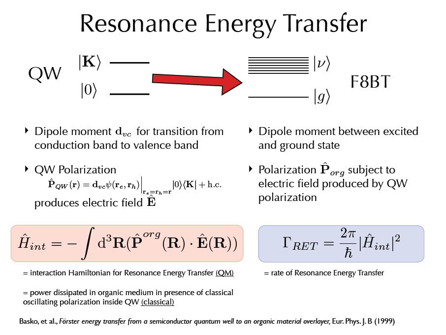
6 Hybrid nanophotonics Nanostructures: light harvesting and light emitting devices Hybrid semiconductor materials:. epitaxial heterostructures/bulk crystals. colloidal QDs and/or organic semiconductors Energy transfer between constituents:. radiative pumping. non-radiative dipole-dipole coupling (RET) RET: Resonance Energy Transfer 6
7 Resonance Energy Transfer
 Appl. Phys. Lett.")
8 Hybrid semiconductor nanostructures Phys. Rev. Lett. 102, (2009) Appl. Phys. Lett. 94, (2009) Advanced Materials 22, (5) 602 (2010) Physical Review Letters 107, (2011) organic-inorganic, colloidal-epitaxial semiconductors weak coupling of electronic transitions 9
 10")
9 (rate R -6 ) 10
. overlap between donor emission and acceptor absorption R n n=6 for point dipoles n=2 2D to 2D 14")
10 Non-radiative energy transfer (RET) Hu et al Quarterly reviews of biophysics 35,1 (2002) LUMO acceptor Donor QW CB ET HOMO VB Energy transfer rate H. Kuhn, J. Chem. Phys. 53, 101 (1970). overlap between donor emission and acceptor absorption R n n=6 for point dipoles n=2 2D to 2D 14
11 Hybrid QW/nanophosphor LEDs 16


12 QW excitations: unbound electron hole pair regime 18
13 19

14 Exciton Transfer in Hybrid Heterostructures (a) CdS ET QW + _ + _ ET k ET ET efficiency: 60K k r Energy Rohrmoser et al Applied Physics Letters 2007
15 QW excitons to J-band excitons Energy transfer rate: A: 4nm B: 6.5nm Population decay (photoluminescence) A: 4nm η A =0.23 and η B =0.39 black QW only red hybrid 25
16 Hybrid Heterostructures in NIR tracking energy transfer at the acceptor site Time correlated single photon counting surface states black organic only red hybrid dashed model Coupled states through non-radiative energy transfer from quantum wells to organic emitter describe transfer dynamics to acceptor (dashed line): Chanyawadee all rates are derived from photoluminescence and fluorescence decay measurements 26 Chanyawadee et al PRB 2008

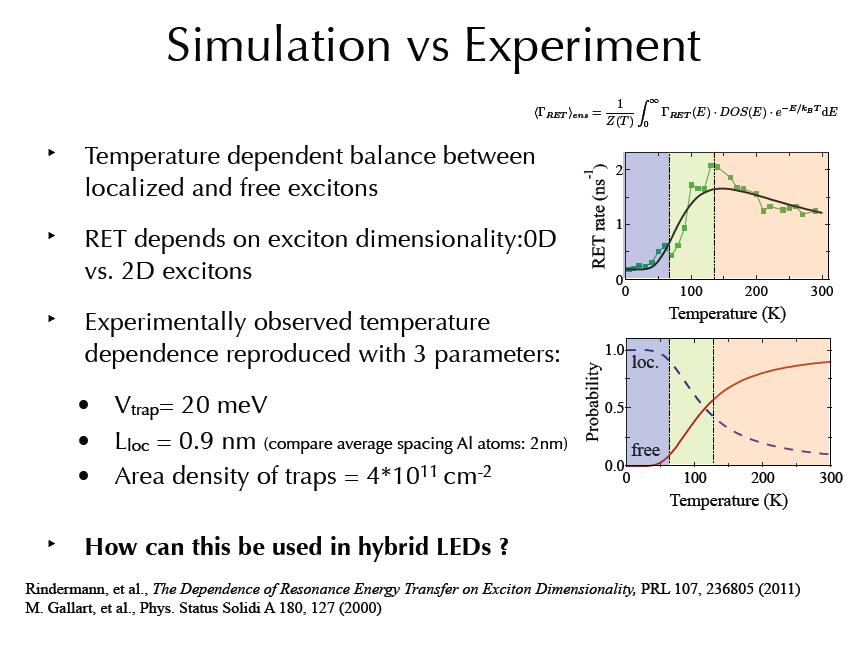
17 Testing the concept of dimensionality 28
18 29
19 30
20 31
21 32
22 35
23 36
24 37
25 38
26 39
 with wave vector k Potential landscape of")

27 Excitons in the QW potential landscape free exciton (2D) with wave vector k Potential landscape of imperfect QW localized exciton (0D) with localization length Lloc Rindermann et al Phys Rev Lett 107,
28 Resonance Energy transfer vs exciton localisation 41
29 Hybrid QD/QW structure NCs QW energy transfer rate minimum barrier width R n patterned QW shorter donor-acceptor distance 43

 Chanyawdee et al; Advanced Materials 22, (5) 602 400")
30 Hybrid colour conversion LED 2 µ m Surface-textured LEDs PL 457 nm Colloidal QDs FL 618 nm PL Intensity (arb. units) Absorption (arb. units) Chanyawdee et al; Advanced Materials 22, (5) Wavelength (nm)

")
31 Fluorescence decay of QDs Unetched QWs: no RET Etched QWs: RET enabled Chanyawdee et al; Advanced Materials 22, (5)
 t knct It () ( e")

")
32 Fluorescence decay of QDs ket ( kqw + ket ) t knct It () ( e e ) k k k NC QW ET Carrier injection due to nonradiative energy transfer Chanyawdee et al; Advanced Materials 22, (5)


33 Hybrid colour conversion LED GB patent Unetched QWs + QDs Etched QWs + QDs 47


34 Hybrid LED with F8BT blue and yellow complimentary colours: --->mix white shallow-etched LED deep-etched LED
35 Hybrid photovoltaics Carrier generation QD layer organic/ncs p-doped layer intrinsic layer n-doped layer Energy transfer Radiative energy transfer Nonradiative energy transfer Carrier extraction pin heterostructure 49


36 Hybrid QD/patterned QW structure 850 nm p+ GaAs p+ AlGaAs i- AlGaAs i- MQW 1350 nm 80x80 mm 2 pattern 20 µ m 2 µ m i- AlGaAs channels n+ GaAs 570 nm width 1.4 µm depth Chanyawadee et al Physical Review Letters 102,
37 Photoluminescence decay of QWs PL Intensity (norm.) flat QW patterned QW QDs + patterned QW Time (ns) Longer rise time indicates energy transfer nqdi (0) keti ( kqdi + keti ) t kqw t I( t) = ( e e ) + f ( t) QDs passivate k k channel k surface QW QDi ETi Chanyawadee et al Physical Review Letters 102,

38 Photocurrent conversion efficiency S ( 1 a H P ) I = I e I a P C 6-fold enhancement of photocurrent conversion efficiency 64% generated from nonradiative energy transfer Chanyawadee et al Physical Review Letters 102, Chanyawadee

39 Hybrid NC/patterned bulk GaAs device 760 nm p+ GaAs p+ AlGaAs p+ GaAs i- GaAs 1850 nm n+ GaAs photoluminescence peak of CdTe NCs : 734 nm PIN device : 823 nm Chanyawadee et al; Applied Physics Letters 94,


40 Hybrid NC/patterned bulk GaAs device RT photocurrent increases in hybrid structures photocurrent enhancement is higher in patterned device Chanyawadee et al; Applied Physics Letters 94,
41 Outlook: RET optoelectronic devices Photovoltaics Silicon HPVs (TSMC), surface treatment, organic sem., blends Lighting application surface passivation/surface-textured LEDs, organic phosphors, organic/qd lasers 55
 Ian Watson, Martin Dawson (Univ.")
 Alexander Eychmuller, (Uni of Dresden) Hiroshi Amano (Nagoya Uni, Japan) Galia Pozina GaN nanofabrication Optical spectroscopy Microscopy")
42 Acknowledgements Laboratories for Hybrid Optoelectronics the people Martin Charlton: Nano-fabrication Industrial collaborations: IBM-Zurich, Luxtaltek, Q-cells David Lidzey (The University of Sheffield) Ian Watson, Martin Dawson (Univ. Strathclyde) Mohamed Henini (University of Nottingham) Dmitry Talapin (University of Chicago) Horst Weller (University of Hamburg) Andrey Rogach (University of Hong Kong) Alexander Eychmuller, (Uni of Dresden) Hiroshi Amano (Nagoya Uni, Japan) Galia Pozina GaN nanofabrication Optical spectroscopy Microscopy Funding: EU-FP7: ITN-Icarus, NoE Nanophotonics for energy efficiency 56
Quantum effects in colloidal nanoparticles. From the beauty of single quantum dot physics to ensemble applications...
 Quantum effects in colloidal nanoparticles From the beauty of single quantum dot physics to ensemble applications... Prof Pavlos Lagoudakis Ioffe 10/06/2013 Colloidal nanocrystals: nano-engineering low
Semiconductor quantum dots
 Semiconductor quantum dots Quantum dots are spherical nanocrystals of semiconducting materials constituted from a few hundreds to a few thousands atoms, characterized by the quantum confinement of the
Time resolved optical spectroscopy methods for organic photovoltaics. Enrico Da Como. Department of Physics, University of Bath
 Time resolved optical spectroscopy methods for organic photovoltaics Enrico Da Como Department of Physics, University of Bath Outline Introduction Why do we need time resolved spectroscopy in OPV? Short
Size-Dependent Biexciton Quantum Yields and Carrier Dynamics of Quasi-
 Supporting Information Size-Dependent Biexciton Quantum Yields and Carrier Dynamics of Quasi- Two-Dimensional Core/Shell Nanoplatelets Xuedan Ma, Benjamin T. Diroll, Wooje Cho, Igor Fedin, Richard D. Schaller,
Semiconductor Quantum Structures And Energy Conversion. Itaru Kamiya Toyota Technological Institute
 Semiconductor Quantum Structures And nergy Conversion April 011, TTI&NCHU Graduate, Special Lectures Itaru Kamiya kamiya@toyota-ti.ac.jp Toyota Technological Institute Outline 1. Introduction. Principle
Ultrafast single photon emitting quantum photonic structures. based on a nano-obelisk
 Ultrafast single photon emitting quantum photonic structures based on a nano-obelisk Je-Hyung Kim, Young-Ho Ko, Su-Hyun Gong, Suk-Min Ko, Yong-Hoon Cho Department of Physics, Graduate School of Nanoscience
Luminescence Process
 Luminescence Process The absorption and the emission are related to each other and they are described by two terms which are complex conjugate of each other in the interaction Hamiltonian (H er ). In an
Electroluminescence from Silicon and Germanium Nanostructures
 Electroluminescence from silicon Silicon Getnet M. and Ghoshal S.K 35 ORIGINAL ARTICLE Electroluminescence from Silicon and Germanium Nanostructures Getnet Melese* and Ghoshal S. K.** Abstract Silicon
Bright and dark exciton transfer in quantum dot arrays Anna Rodina
 Bright and dark exciton transfer in quantum dot arrays Anna Rodina Ioffe Institute, St. Petersburg, Russia Collaboration and publications: [1] A. N. Poddubny, A. V. Rodina, Nonradiative and radiative Förster
Luminescence basics. Slide # 1
 Luminescence basics Types of luminescence Cathodoluminescence: Luminescence due to recombination of EHPs created by energetic electrons. Example: CL mapping system Photoluminescence: Luminescence due to
Stimulated Emission Devices: LASERS
 Stimulated Emission Devices: LASERS 1. Stimulated Emission and Photon Amplification E 2 E 2 E 2 hυ hυ hυ In hυ Out hυ E 1 E 1 E 1 (a) Absorption (b) Spontaneous emission (c) Stimulated emission The Principle
Fabrication / Synthesis Techniques
 Quantum Dots Physical properties Fabrication / Synthesis Techniques Applications Handbook of Nanoscience, Engineering, and Technology Ch.13.3 L. Kouwenhoven and C. Marcus, Physics World, June 1998, p.35
Scienza e Tecnologia dei Materiali Ceramici. Modulo 2: Materiali Nanostrutturati
 Università degli Studi di Trieste Dipartimento di Ingegneria e Architettura A.A. 2016-2017 Scienza e Tecnologia dei Materiali Ceramici Modulo 2: Materiali Nanostrutturati - Lezione 5 - Vanni Lughi vlughi@units.it
Physics and Material Science of Semiconductor Nanostructures
 Physics and Material Science of Semiconductor Nanostructures PHYS 570P Prof. Oana Malis Email: omalis@purdue.edu Course website: http://www.physics.purdue.edu/academic_programs/courses/phys570p/ 1 Course
Solar Cell Materials and Device Characterization
 Solar Cell Materials and Device Characterization April 3, 2012 The University of Toledo, Department of Physics and Astronomy SSARE, PVIC Principles and Varieties of Solar Energy (PHYS 4400) and Fundamentals
III-V nanostructured materials synthesized by MBE droplet epitaxy
 III-V nanostructured materials synthesized by MBE droplet epitaxy E.A. Anyebe 1, C. C. Yu 1, Q. Zhuang 1,*, B. Robinson 1, O Kolosov 1, V. Fal ko 1, R. Young 1, M Hayne 1, A. Sanchez 2, D. Hynes 2, and
(b) Spontaneous emission. Absorption, spontaneous (random photon) emission and stimulated emission.
 Spontaneous emission. Absorption, spontaneous (random photon) emission and stimulated emission.") Lecture 10 Stimulated Emission Devices Lasers Stimulated emission and light amplification Einstein coefficients Optical fiber amplifiers Gas laser and He-Ne Laser The output spectrum of a gas laser Laser
Lecture 10 Stimulated Emission Devices Lasers Stimulated emission and light amplification Einstein coefficients Optical fiber amplifiers Gas laser and He-Ne Laser The output spectrum of a gas laser Laser
Fundamentals of Nanoelectronics: Basic Concepts
 Fundamentals of Nanoelectronics: Basic Concepts Sławomir Prucnal FWIM Page 1 Introduction Outline Electronics in nanoscale Transport Ohms law Optoelectronic properties of semiconductors Optics in nanoscale
Optical Investigation of the Localization Effect in the Quantum Well Structures
 Department of Physics Shahrood University of Technology Optical Investigation of the Localization Effect in the Quantum Well Structures Hamid Haratizadeh hamid.haratizadeh@gmail.com IPM, SCHOOL OF PHYSICS,
Enhancing the Rate of Spontaneous Emission in Active Core-Shell Nanowire Resonators
 Chapter 6 Enhancing the Rate of Spontaneous Emission in Active Core-Shell Nanowire Resonators 6.1 Introduction Researchers have devoted considerable effort to enhancing light emission from semiconductors
Semiconductor Quantum Dots
 Semiconductor Quantum Dots M. Hallermann Semiconductor Physics and Nanoscience St. Petersburg JASS 2005 Outline Introduction Fabrication Experiments Applications Porous Silicon II-VI Quantum Dots III-V
Emission Spectra of the typical DH laser
 Emission Spectra of the typical DH laser Emission spectra of a perfect laser above the threshold, the laser may approach near-perfect monochromatic emission with a spectra width in the order of 1 to 10
Optical and Terahertz Characterization of Be-Doped GaAs/AlAs Multiple Quantum Wells
 Vol. 107 (2005) ACTA PHYSICA POLONICA A No. 2 Proceedings of the 12th International Symposium UFPS, Vilnius, Lithuania 2004 Optical and Terahertz Characterization of Be-Doped GaAs/AlAs Multiple Quantum
Electronic and Optoelectronic Properties of Semiconductor Structures
 Electronic and Optoelectronic Properties of Semiconductor Structures Jasprit Singh University of Michigan, Ann Arbor CAMBRIDGE UNIVERSITY PRESS CONTENTS PREFACE INTRODUCTION xiii xiv 1.1 SURVEY OF ADVANCES
Seminars in Nanosystems - I
 Seminars in Nanosystems - I Winter Semester 2011/2012 Dr. Emanuela Margapoti Emanuela.Margapoti@wsi.tum.de Dr. Gregor Koblmüller Gregor.Koblmueller@wsi.tum.de Seminar Room at ZNN 1 floor Topics of the
In a metal, how does the probability distribution of an electron look like at absolute zero?
 1 Lecture 6 Laser 2 In a metal, how does the probability distribution of an electron look like at absolute zero? 3 (Atom) Energy Levels For atoms, I draw a lower horizontal to indicate its lowest energy
Development of Dual MQW Region LEDs for General Illumination
 Mater. Res. Soc. Symp. Proc. Vol. 831 2005 Materials Research Society E10.3.1 Development of Dual MQW Region LEDs for General Illumination David Brackin Nicol 1, Ali Asghar 1, Martin Strassburg 1,3, My
GeSi Quantum Dot Superlattices
 GeSi Quantum Dot Superlattices ECE440 Nanoelectronics Zheng Yang Department of Electrical & Computer Engineering University of Illinois at Chicago Nanostructures & Dimensionality Bulk Quantum Walls Quantum
Three-Dimensional Silicon-Germanium Nanostructures for Light Emitters and On-Chip Optical. Interconnects
 Three-Dimensional Silicon-Germanium Nanostructures for Light Emitters and On-Chip Optical eptember 2011 Interconnects Leonid Tsybeskov Department of Electrical and Computer Engineering New Jersey Institute
Semiconductors and Optoelectronics. Today Semiconductors Acoustics. Tomorrow Come to CH325 Exercises Tours
 Semiconductors and Optoelectronics Advanced Physics Lab, PHYS 3600 Don Heiman, Northeastern University, 2017 Today Semiconductors Acoustics Tomorrow Come to CH325 Exercises Tours Semiconductors and Optoelectronics
smal band gap Saturday, April 9, 2011
 small band gap upper (conduction) band empty small gap valence band filled 2s 2p 2s 2p hybrid (s+p)band 2p no gap 2s (depend on the crystallographic orientation) extrinsic semiconductor semi-metal electron
Nanotechnology and Solar Energy. Solar Electricity Photovoltaics. Fuel from the Sun Photosynthesis Biofuels Split Water Fuel Cells
 Nanotechnology and Solar Energy Solar Electricity Photovoltaics Fuel from the Sun Photosynthesis Biofuels Split Water Fuel Cells Solar cell A photon from the Sun generates an electron-hole pair in a semiconductor.
Optical spectroscopy of carrier dynamics in semiconductor nanostructures de Jong, E.M.L.D.
 UvA-DARE (Digital Academic Repository) Optical spectroscopy of carrier dynamics in semiconductor nanostructures de Jong, E.M.L.D. Link to publication Citation for published version (APA): de Jong, EM-LD.
Progress Report to AOARD
 Progress Report to AOARD C. C. (Chih-Chung) Yang The Graduate Institute of Electro-Optical Engineering National Taiwan University No. 1, Roosevelt Road, Section 4, Taipei, Taiwan (phone) 886-2-23657624
vapour deposition. Raman peaks of the monolayer sample grown by chemical vapour
 Supplementary Figure 1 Raman spectrum of monolayer MoS 2 grown by chemical vapour deposition. Raman peaks of the monolayer sample grown by chemical vapour deposition (S-CVD) are peak which is at 385 cm
Spontaneous Emission and Ultrafast Carrier Relaxation in InGaN Quantum Well with Metal Nanoparticles. Meg Mahat and Arup Neogi
 Spontaneous Emission and Ultrafast Carrier Relaxation in InGaN Quantum Well with Metal Nanoparticles Meg Mahat and Arup Neogi Department of Physics, University of North Texas, Denton, Tx, 76203 ABSTRACT
what happens if we make materials smaller?
 what happens if we make materials smaller? IAP VI/10 ummer chool 2007 Couvin Prof. ns outline Introduction making materials smaller? ynthesis how do you make nanomaterials? Properties why would you make
Self-Assembled InAs Quantum Dots
 Self-Assembled InAs Quantum Dots Steve Lyon Department of Electrical Engineering What are semiconductors What are semiconductor quantum dots How do we make (grow) InAs dots What are some of the properties
Basic cell design. Si cell
 Basic cell design Si cell 1 Concepts needed to describe photovoltaic device 1. energy bands in semiconductors: from bonds to bands 2. free carriers: holes and electrons, doping 3. electron and hole current:
Nanophysics: Main trends
 Nano-opto-electronics Nanophysics: Main trends Nanomechanics Main issues Light interaction with small structures Molecules Nanoparticles (semiconductor and metallic) Microparticles Photonic crystals Nanoplasmonics
2D MBE Activities in Sheffield. I. Farrer, J. Heffernan Electronic and Electrical Engineering The University of Sheffield
 2D MBE Activities in Sheffield I. Farrer, J. Heffernan Electronic and Electrical Engineering The University of Sheffield Outline Motivation Van der Waals crystals The Transition Metal Di-Chalcogenides
Development and application for X-ray excited optical luminescence (XEOL) technology at STXM beamline of SSRF
 technology at STXM beamline of SSRF") Development and application for X-ray excited optical luminescence (XEOL) technology at STXM beamline of SSRF Content Introduction to XEOL Application of XEOL Development and Application of XEOL in STXM
Development and application for X-ray excited optical luminescence (XEOL) technology at STXM beamline of SSRF Content Introduction to XEOL Application of XEOL Development and Application of XEOL in STXM
Sheng S. Li. Semiconductor Physical Electronics. Second Edition. With 230 Figures. 4) Springer
 Springer") Sheng S. Li Semiconductor Physical Electronics Second Edition With 230 Figures 4) Springer Contents Preface 1. Classification of Solids and Crystal Structure 1 1.1 Introduction 1 1.2 The Bravais Lattice
Sheng S. Li Semiconductor Physical Electronics Second Edition With 230 Figures 4) Springer Contents Preface 1. Classification of Solids and Crystal Structure 1 1.1 Introduction 1 1.2 The Bravais Lattice
ISSN Review. Progress to a Gallium-Arsenide Deep-Center Laser
 Materials 2009, 2, 1599-1635; doi:10.3390/ma2041599 OPEN ACCESS materials ISSN 1996-1944 www.mdpi.com/journal/materials Review Progress to a Gallium-Arsenide Deep-Center Laser Janet L. Pan Yale University,
Plasmon-enhanced yellow light emission in hybrid nanostructures formed by fluorescent molecules and polymer
 Nano Energy (]]]]) ], ]]] ]]] Available online at www.sciencedirect.com journal homepage: www.elsevier.com/locate/nanoenergy Plasmon-enhanced yellow light emission in hybrid nanostructures formed by fluorescent
Spin Lifetime Measurements in MBE-Grown GaAs Epilayers
 phys. stat. sol. (b) 233, No. 3, 445 452 (2002) Spin Lifetime Measurements in MBE-Grown GaAs Epilayers J. S. Colton 1 ), T. A. Kennedy, A. S. Bracker, and D. Gammon Naval Research Laboratory, Washington
Optical Nonlinearities in Quantum Wells
 Harald Schneider Institute of Ion-Beam Physics and Materials Research Semiconductor Spectroscopy Division Rosencher s Optoelectronic Day Onéra 4.05.011 Optical Nonlinearities in Quantum Wells Harald Schneider
Lecture 6: Individual nanoparticles, nanocrystals and quantum dots
 Lecture 6: Individual nanoparticles, nanocrystals and quantum dots Definition of nanoparticle: Size definition arbitrary More interesting: definition based on change in physical properties. Size smaller
Mesoporous titanium dioxide electrolyte bulk heterojunction
 Mesoporous titanium dioxide electrolyte bulk heterojunction The term "bulk heterojunction" is used to describe a heterojunction composed of two different materials acting as electron- and a hole- transporters,
Quantum Dots for Advanced Research and Devices
 Quantum Dots for Advanced Research and Devices spectral region from 450 to 630 nm Zero-D Perovskite Emit light at 520 nm ABOUT QUANTUM SOLUTIONS QUANTUM SOLUTIONS company is an expert in the synthesis
interband transitions in semiconductors M. Fox, Optical Properties of Solids, Oxford Master Series in Condensed Matter Physics
 interband transitions in semiconductors M. Fox, Optical Properties of Solids, Oxford Master Series in Condensed Matter Physics interband transitions in quantum wells Atomic wavefunction of carriers in
Widely Tunable and Intense Mid-Infrared PL Emission from Epitaxial Pb(Sr)Te Quantum Dots in a CdTe Matrix
Te Quantum Dots in a CdTe Matrix") Widely Tunable and Intense Mid-Infrared PL Emission from Epitaxial Pb(Sr)Te Quantum Dots in a Matrix S. Kriechbaumer 1, T. Schwarzl 1, H. Groiss 1, W. Heiss 1, F. Schäffler 1,T. Wojtowicz 2, K. Koike 3,
Widely Tunable and Intense Mid-Infrared PL Emission from Epitaxial Pb(Sr)Te Quantum Dots in a Matrix S. Kriechbaumer 1, T. Schwarzl 1, H. Groiss 1, W. Heiss 1, F. Schäffler 1,T. Wojtowicz 2, K. Koike 3,
Semiconductor Quantum Dot Nanostructures and their Roles in the Future of Photonics
 550 Brazilian Journal of Physics, vol. 34, no. 2B, June, 2004 Semiconductor Quantum Dot Nanostructures and their Roles in the Future of Photonics S. Fafard, K. Hinzer, and C. N. Allen Institute for Microstructural
Electromagnetically Induced Transparency (EIT) via Spin Coherences in Semiconductor
 via Spin Coherences in Semiconductor") Electromagnetically Induced Transparency (EIT) via Spin Coherences in Semiconductor Hailin Wang Oregon Center for Optics, University of Oregon, USA Students: Shannon O Leary Susanta Sarkar Yumin Shen Phedon
Electromagnetically Induced Transparency (EIT) via Spin Coherences in Semiconductor Hailin Wang Oregon Center for Optics, University of Oregon, USA Students: Shannon O Leary Susanta Sarkar Yumin Shen Phedon
Supplementary Materials
 Supplementary Materials Sample characterization The presence of Si-QDs is established by Transmission Electron Microscopy (TEM), by which the average QD diameter of d QD 2.2 ± 0.5 nm has been determined
CH676 Physical Chemistry: Principles and Applications. CH676 Physical Chemistry: Principles and Applications
 CH676 Physical Chemistry: Principles and Applications Crystal Structure and Chemistry Synthesis of Tetrahexahedral Platinum Nanocrystals with High-Index Facets and High Electro-Oxidation Activity Na Tian
Novel materials and nanostructures for advanced optoelectronics
 Novel materials and nanostructures for advanced optoelectronics Q. Zhuang, P. Carrington, M. Hayne, A Krier Physics Department, Lancaster University, UK u Brief introduction to Outline Lancaster University
Chapter 6: Light-Emitting Diodes
 Chapter 6: Light-Emitting Diodes Photoluminescence and electroluminescence Basic transitions Luminescence efficiency Light-emitting diodes Internal quantum efficiency External quantum efficiency Device
Spectroscopy of. Semiconductors. Luminescence OXFORD IVAN PELANT. Academy ofsciences of the Czech Republic, Prague JAN VALENTA
 Luminescence Spectroscopy of Semiconductors IVAN PELANT Institute ofphysics, v.v.i. Academy ofsciences of the Czech Republic, Prague JAN VALENTA Department of Chemical Physics and Optics Charles University,
Influence of Plasmonic Array Geometry on Energy Transfer from a. Quantum Well to a Quantum Dot Layer
 Electronic Supplementary Material (ESI) for Nanoscale. This journal is The Royal Society of Chemistry 2016 Influence of Plasmonic Array Geometry on Energy Transfer from a Quantum Well to a Quantum Dot
Simple strategy for enhancing terahertz emission from coherent longitudinal optical phonons using undoped GaAs/n-type GaAs epitaxial layer structures
 Presented at ISCS21 June 4, 21 Session # FrP3 Simple strategy for enhancing terahertz emission from coherent longitudinal optical phonons using undoped GaAs/n-type GaAs epitaxial layer structures Hideo
Plasmon enhanced UV electroluminescence in SiO 2 with percolating conduction sustained by free-exciton emitting SnO 2 nanoparticles
 Dipartimento di Scienza dei Materiali Università di Milano-Bicocca TITLE Plasmon enhanced UV electroluminescence in O 2 with percolating conduction sustained by free-exciton emitting SnO 2 nanoparticles
Single Emitter Detection with Fluorescence and Extinction Spectroscopy
 Single Emitter Detection with Fluorescence and Extinction Spectroscopy Michael Krall Elements of Nanophotonics Associated Seminar Recent Progress in Nanooptics & Photonics May 07, 2009 Outline Single molecule
Chemistry Instrumental Analysis Lecture 8. Chem 4631
 Chemistry 4631 Instrumental Analysis Lecture 8 UV to IR Components of Optical Basic components of spectroscopic instruments: stable source of radiant energy transparent container to hold sample device
Electrically Driven Polariton Devices
 Electrically Driven Polariton Devices Pavlos Savvidis Dept of Materials Sci. & Tech University of Crete / FORTH Polariton LED Rome, March 18, 211 Outline Polariton LED device operating up to room temperature
Nanostructured Semiconductor Crystals -- Building Blocks for Solar Cells: Shapes, Syntheses, Surface Chemistry, Quantum Confinement Effects
 Nanostructured Semiconductor Crystals -- Building Blocks for Solar Cells: Shapes, Syntheses, Surface Chemistry, Quantum Confinement Effects April 1,2014 The University of Toledo, Department of Physics
Photonic Crystal Nanocavities for Efficient Light Confinement and Emission
 Journal of the Korean Physical Society, Vol. 42, No., February 2003, pp. 768 773 Photonic Crystal Nanocavities for Efficient Light Confinement and Emission Axel Scherer, T. Yoshie, M. Lončar, J. Vučković
Chapter 6 Photoluminescence Spectroscopy
 Chapter 6 Photoluminescence Spectroscopy Course Code: SSCP 4473 Course Name: Spectroscopy & Materials Analysis Sib Krishna Ghoshal (PhD) Advanced Optical Materials Research Group Physics Department, Faculty
Electron Energy, E E = 0. Free electron. 3s Band 2p Band Overlapping energy bands. 3p 3s 2p 2s. 2s Band. Electrons. 1s ATOM SOLID.
 Electron Energy, E Free electron Vacuum level 3p 3s 2p 2s 2s Band 3s Band 2p Band Overlapping energy bands Electrons E = 0 1s ATOM 1s SOLID In a metal the various energy bands overlap to give a single
University of Louisville - Department of Chemistry, Louisville, KY; 2. University of Louisville Conn Center for renewable energy, Louisville, KY; 3
 Ultrafast transient absorption spectroscopy investigations of charge carrier dynamics of methyl ammonium lead bromide (CH 3 NH 3 PbBr 3 ) perovskite nanostructures Hamzeh Telfah 1 ; Abdelqader Jamhawi
Physics and Material Science of Semiconductor Nanostructures
 Physics and Material Science of Semiconductor Nanostructures PHYS 570P Prof. Oana Malis Email: omalis@purdue.edu Course website: http://www.physics.purdue.edu/academic_programs/courses/phys570p/ 1 Introduction
CHARGE CARRIERS PHOTOGENERATION. Maddalena Binda Organic Electronics: principles, devices and applications Milano, November 23-27th, 2015
 CHARGE CARRIERS PHOTOGENERATION Maddalena Binda Organic Electronics: principles, devices and applications Milano, November 23-27th, 2015 Charge carriers photogeneration: what does it mean? Light stimulus
Multiple Exciton Generation in Quantum Dots. James Rogers Materials 265 Professor Ram Seshadri
 Multiple Exciton Generation in Quantum Dots James Rogers Materials 265 Professor Ram Seshadri Exciton Generation Single Exciton Generation in Bulk Semiconductors Multiple Exciton Generation in Bulk Semiconductors
Q. Shen 1,2) and T. Toyoda 1,2)
 and T. Toyoda 1,2)") Photosensitization of nanostructured TiO 2 electrodes with CdSe quntum dots: effects of microstructure in substrates Q. Shen 1,2) and T. Toyoda 1,2) Department of Applied Physics and Chemistry 1), and
Photosensitization of nanostructured TiO 2 electrodes with CdSe quntum dots: effects of microstructure in substrates Q. Shen 1,2) and T. Toyoda 1,2) Department of Applied Physics and Chemistry 1), and
Part I. Nanostructure design and structural properties of epitaxially grown quantum dots and nanowires
 Part I Nanostructure design and structural properties of epitaxially grown quantum dots and nanowires 1 Growth of III V semiconductor quantum dots C. Schneider, S. Höfling and A. Forchel 1.1 Introduction
PHOTOVOLTAICS Fundamentals
 PHOTOVOLTAICS Fundamentals PV FUNDAMENTALS Semiconductor basics pn junction Solar cell operation Design of silicon solar cell SEMICONDUCTOR BASICS Allowed energy bands Valence and conduction band Fermi
Semiconductor Physical Electronics
 Semiconductor Physical Electronics Sheng S. Li Department of Electrical Engineering University of Florida Gainesville, Florida Plenum Press New York and London Contents CHAPTER 1. Classification of Solids
Optical Science of Nano-graphene (graphene oxide and graphene quantum dot) Introduction of optical properties of nano-carbon materials
 Introduction of optical properties of nano-carbon materials") Optical Science of Nano-graphene (graphene oxide and graphene quantum dot) J Kazunari Matsuda Institute of Advanced Energy, Kyoto University Introduction of optical properties of nano-carbon materials
Optical Science of Nano-graphene (graphene oxide and graphene quantum dot) J Kazunari Matsuda Institute of Advanced Energy, Kyoto University Introduction of optical properties of nano-carbon materials
Thermionic Current Modeling and Equivalent Circuit of a III-V MQW P-I-N Photovoltaic Heterostructure
 Thermionic Current Modeling and Equivalent Circuit of a III-V MQW P-I-N Photovoltaic Heterostructure ARGYRIOS C. VARONIDES Physics and Electrical Engineering Department University of Scranton 800 Linden
doi: /PhysRevLett
 doi: 10.1103/PhysRevLett.77.494 Luminescence Hole Burning and Quantum Size Effect of Charged Excitons in CuCl Quantum Dots Tadashi Kawazoe and Yasuaki Masumoto Institute of Physics and Center for TARA
Semiconductor device structures are traditionally divided into homojunction devices
 0. Introduction: Semiconductor device structures are traditionally divided into homojunction devices (devices consisting of only one type of semiconductor material) and heterojunction devices (consisting
Charge Excitation. Lecture 4 9/20/2011 MIT Fundamentals of Photovoltaics 2.626/2.627 Fall 2011 Prof. Tonio Buonassisi
 Charge Excitation Lecture 4 9/20/2011 MIT Fundamentals of Photovoltaics 2.626/2.627 Fall 2011 Prof. Tonio Buonassisi 1 2.626/2.627 Roadmap You Are Here 2 2.626/2.627: Fundamentals Every photovoltaic device
Semiconductor. Byungwoo Park. Department of Materials Science and Engineering Seoul National University.
 Semiconductor Byungwoo Park Department of Materials Science and Engineering Seoul National University http://bp.snu.ac.kr http://bp.snu.ac.kr Semiconductors Kittel, Solid State Physics (Chapters 7 and
SUPPLEMENTARY INFORMATION
 doi:10.1038/nature12036 We provide in the following additional experimental data and details on our demonstration of an electrically pumped exciton-polariton laser by supplementing optical and electrical
Opto-electronic Characterization of Perovskite Thin Films & Solar Cells
 Opto-electronic Characterization of Perovskite Thin Films & Solar Cells Arman Mahboubi Soufiani Supervisors: Prof. Martin Green Prof. Gavin Conibeer Dr. Anita Ho-Baillie Dr. Murad Tayebjee 22 nd June 2017
Intraband emission of GaN quantum dots at λ =1.5 μm via resonant Raman scattering
 Intraband emission of GaN quantum dots at λ =1.5 μm via resonant Raman scattering L. Nevou, F. H. Julien, M. Tchernycheva, J. Mangeney Institut d Electronique Fondamentale, UMR CNRS 8622, University Paris-Sud
Chapter 4. Photodetectors
 Chapter 4 Photodetectors Types of photodetectors: Photoconductos Photovoltaic Photodiodes Avalanche photodiodes (APDs) Resonant-cavity photodiodes MSM detectors In telecom we mainly use PINs and APDs.
Title: Ultrafast photocurrent measurement of the escape time of electrons and holes from
 Title: Ultrafast photocurrent measurement of the escape time of electrons and holes from carbon nanotube PN junction photodiodes Authors: Nathaniel. M. Gabor 1,*, Zhaohui Zhong 2, Ken Bosnick 3, Paul L.
Hybrid indium phosphide-on-silicon nanolaser diode
 In the format provided by the authors and unedited. DOI: 10.1038/NPHOTON.2017.56 Hybrid indium phosphide-on-silicon nanolaser diode Guillaume Crosnier 1,2, Dorian Sanchez 2, Sophie Bouchoule 2, Paul Monnier
Physics of Semiconductors
 Physics of Semiconductors 9 th 2016.6.13 Shingo Katsumoto Department of Physics and Institute for Solid State Physics University of Tokyo Site for uploading answer sheet Outline today Answer to the question
Supplemental Materials for. Interlayer Exciton Optoelectronics in a 2D Heterostructure p-n Junction
 Supplemental Materials for Interlayer Exciton Optoelectronics in a 2D Heterostructure p-n Junction Jason S. Ross 1, Pasqual Rivera 2, John Schaibley 2, Eric Lee-Wong 2, Hongyi Yu 3, Takashi Taniguchi 4,
SELF-ASSEMBLED QUANTUM DOTS FOR OPTOELECTRONIC DEVICES: PROGRESS AND CHALLENGES
 SELF-ASSEMBLED QUANTUM DOTS FOR OPTOELECTRONIC DEVICES: PROGRESS AND CHALLENGES M.Henini School of Physics and Astronomy, University of Nottingham, Nottingham NG7 2RD, U.K. Tel/Fax: +44 115 9515195/9515180
Senior Project Thesis Senior Project Committee, Department of Physics, Case Western Reserve University
 Liquid Crystal Semiconductor Nanostructures Richard Metzger,Department of Physics, Case Western Reserve University Nick Lind, Department of Physics, Case Western Reserve University Professor K. Singer,
Excitonics of semiconductor quantum dots and wires for lighting and displays
 Laser Photonics Rev. 8, No. 1, 73 93 (2014) / DOI 10.1002/lpor.201300024 LASER & PHOTONICS Abstract In the past two decades, semiconductor quantum dots and wires have developed into new, promising classes
Tianle Guo, 1 Siddharth Sampat, 1 Kehao Zhang, 2 Joshua A. Robinson, 2 Sara M. Rupich, 3 Yves J. Chabal, 3 Yuri N. Gartstein, 1 and Anton V.
 SUPPLEMENTARY INFORMATION for Order of magnitude enhancement of monolayer MoS photoluminescence due to near-field energy influx from nanocrystal films Tianle Guo, Siddharth Sampat, Kehao Zhang, Joshua
Supplementary Figure 1 Interlayer exciton PL peak position and heterostructure twisting angle. a, Photoluminescence from the interlayer exciton for
 Supplementary Figure 1 Interlayer exciton PL peak position and heterostructure twisting angle. a, Photoluminescence from the interlayer exciton for six WSe 2 -MoSe 2 heterostructures under cw laser excitation
Supplementary Information for
 Supplementary Information for Multi-quantum well nanowire heterostructures for wavelength-controlled lasers Fang Qian 1, Yat Li 1 *, Silvija Gradečak 1, Hong-Gyu Park 1, Yajie Dong 1, Yong Ding 2, Zhong
Ultrafast carrier dynamics in InGaN MQW laser diode
 Invited Paper Ultrafast carrier dynamics in InGaN MQW laser diode Kian-Giap Gan* a, Chi-Kuang Sun b, John E. Bowers a, and Steven P. DenBaars a a Department of Electrical and Computer Engineering, University
Introduction to Semiconductor Integrated Optics
 Introduction to Semiconductor Integrated Optics Hans P. Zappe Artech House Boston London Contents acknowledgments reface itroduction Chapter 1 Basic Electromagnetics 1 1.1 General Relationships 1 1.1.1
Flexible Organic Photovoltaics Employ laser produced metal nanoparticles into the absorption layer 1. An Introduction
 Flexible Organic Photovoltaics Employ laser produced metal nanoparticles into the absorption layer 1. An Introduction Among the renewable energy sources that are called to satisfy the continuously increased