Part II Low dimensional carbon materials Carbon
|
|
|
- Beverly Fisher
- 5 years ago
- Views:
Transcription
1 Part II Low dimensional carbon materials Carbon nanotubes (CNTs) and Graphene
2 Outline Carbon nanomaterials Types of carbon nanomaterials Graphene and CNT Introduction Synthesis Specific topics Application 2
3 Carbon Nanomaterials 3D 2D 1D 0D Graphite Diamond Graphene Carbon nanotube Fullerene 3


4 3D Diamond and Graphite Cabon-related nanomaterials (2010 Nobel prize in physics) 2D Graphene discovered by Prof. Ijima, 1991 (1996 Nobel priz in Chemistry) en.wikipedia.org craigbanksresearch.com grapheneindustries.com 1D Carbon nanotube 0D Blkbll(C Bulkyball(C 60 )
5 2 1. Introduction of CNT 5
 1991: CNTs were discovered by")

6 CNT History 1952: Radushkevich hand Lukyanovich hfound nano sized carbon fibers (Russian) 1991: CNTs were discovered by Prof. Ijima and named 1992: Theoretical predictions of the electronic properties of SWCNT 1997: First CNT transistor 6


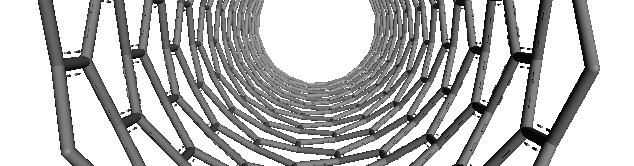


7 Structure of CNT Single Walled CNT (SWCNT) Multi Walled CNT (MWCNT) (10,0) (6,0)+(15,0)+(24,0) The interlayer distance in multi walled nanotubes is close to the distance between graphene layers in graphite, approximately 3.4 Å. 7


 Z")


8 Structure of CNT Similar to GNRs, we should take the chirality of CNTs into account (10,0) Z CNT (6,6) A CNT 8
9 Physical Properties of CNT Semiconductor or metal. (depending di on the chiral angle) Excellent mechanical properties Excellent electrical transport (ballistic transport) Excellent thermal conductivity Difficulty Control the chiralty


10 1 D nanomaterials (Carbon nanotube) Discovered by Iijima (1991)
11 Band Structures of CNT (10,10) (9,0) (10,0) Band structures of (a) (10,10) 10) (b) (9,0) (c) (10,0) 0) CNTs A. Baskin et al., Scientific Reports 1, 36 (2011) 11
12 Electronic Properties of CNT Energy gap changes with chirality and diameter Tight binding calculations Experiments Nature 391,62, 1998


13 Structural Materials Due to the outstanding mechanical properties and light weighted, ih dcnt is a potential ilmaterial for some special usages Space elevator Bulletproof cloth, shield, glass Bicycle components 13
14 Mechanical Properties CNT is one of the strongest materials in nature Very strong in the axial direction Young s modulus (GPa) Tensile strength (GPa) Elongation at break (%) SWCNT > Steel Diamond Very hard; even harder than the diamond Bulk modulus (GPa) SWCNT Steel 160 Diamond 442 Belluci, S. et al., Phys. Status Solidi C 2 (1), 34 (2005) Sinnott, S.B. et al., Crit. Rev. Solid State 26 (3), 145 (2001) 14
15 Electronic Properties Tang, Z. K. et al., Science 292 (5526), 2462 (2001) 15


16 Interconnects Similar to GNRs, CNTs are potential materials to replace metal (such that Cu, Au) as non metal high conductivity interconnects in the integrated circuits Y. Zhao et al., Scientific Reports 1, 83 (2011) 16
17 Transport of CNT Nanotube field effect transistor Ambipolar Electrical Transport in Semiconducting Single Wall Carbon Nanotubes A. Jorio, et. al. Topics Appl. Physics 111,
: 3817 Cao. J., et. al. Nature Materials 4, 745 749 (2005) 18")
18 CNT Transistor Various type of CNT transistors had been developed Back gated Wrap around around gate Sander J. Tans, et. al., Nature 1998, 393, Top gated Chen, Z., et. al., IEEE ELECTRON DEVICE LETTERS, VOL. 29, NO. 2, Suspended Wind, S. J. et. al., 2002 Applied Physics Letters 80 (20): 3817 Cao. J., et. al. Nature Materials 4, (2005) 18


19 Designs of CNT Transistors Back gated Top gated First CNT FET be invented. The process is easy, but there are many drawbacks 1. Contact resistance exists between metal and CNT 2. Hard to switch off using low voltage 3. Poor contact between SiO 2 and CNT Advanced designs from back gate FET. The thinner gate dielectric lower the switch off voltage, which is the main advantage of the top gate FET. 19


 Developed in")


20 Designs of CNT Transistors Wrap around around gate Suspended Developed in This design 1. Improvethe on/off ratio and the performance 2. Reduce the leakage current Z. Chen et al., EDL 29 (2), 183 (2008) J. Cao et al., Nature Materials 4, 745 (2005) Developed in This design reduces the scattering at the interface of the CNT substrate. However, materials of devices are limited. It is only for studying the properties p of clean CNT and cannot be commercialized. 20

 (S 22 )")


21 Optical Properties of CNT (M 11 ) (S 11 ) (S 22 ) Van Hove singularity: The discontinuity of DOS of 1D materials 21


22 Optical Properties Because of the sharp transitions, we can selectively excite (n,m) CNT; namely, we can detect optical signals in order to identify (n,m) CNT Kataura plot R. B. Weisman and S. M. Bachilo, Nano Lett. 3 (9), 1235 (2003) 22
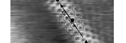
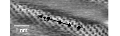
23 Photoluminescence of CNT Process of PL 1. Excite S 22 (C 2 V 2 ) and create the exciton pair 2. Relax to C 1 and V 1 respectively 3. Recombine and emit light with S 11 (C 1 VV 1 ) energy An important tools for characterizing semiconducting CNT R. B. Weisman and S. M. Bachilo, Nano Lett. 3, 1235 (2003) 23
24 PL Mapping of CNT S 22 of [9,8] CNT S 11 of [9,8] CNT 24


 Energy and Environmental")
25 100 Applications: Optical and Electrical Properties of SWNT Electrode ) Trans smittance (% %) Transm mittance (% Filtration Volume 0.5 ml 075ml ml 2 ml 3 ml ITO (a) Wavelength (nm) SWNT untreated SWNT HNO 3 treated SWNT electrode has high flexibility and excellent mechanical strength Sheet resistance of SWNT electrode can be further reduced by HNO 3 treatment Sheet resistance it ~100 Ω/sq with 75% 550nm Sheet Resistance (Ω/sq) Energy and Environmental Science, , (2011) 25


 6 4 2")


 Jsc (ma) Fill Factor")

 CNT (1D)")

26 Nanocarbon based polymer solar cells by solution processes Cocktail nanocarbon polymer solar cell! PCBM (0D) Cur rrent Density (ma/cm 2 ) SWNT without GO Layer SWNT with GO Layer Voltage (V) SWNT Voc (V) Jsc (ma) Fill Factor PCE (%) Without GO % With GO % GO (2D) CNT (1D) ITO/PEDOT:PSS % Energy and Environmental Science, 4,3521, (2011) 26


27 Carbon Nanotube on photovoltaic and LED applications High transparency on visible and NIR range Good d conductivity Flexible Silicon CNT heterojunction solar cell Top Emission OLED 27 Jia, Y. et. al., Nano Lett, 2011, 11, Chien, Y. M. et. al, Nanotechnology, 2010, 21,

, 5182")


28 Other Applications Fuel cells Store H 2 in CNT Gas detector Wang, S. Et. al., J. Am. Chem. Soc., 2011, 133 (14), 5182 Molecules adsorb on the channel of CNT FET, modifying the electrical properties of CNT G. Lu, LE L.E. Ocola J. Chen, Adv. Mt Mater, 2009, 21,


29 Applications of Carbon Nanotube Field Emitter Hydrogen Storage Li-ion battery anode Logic gate by IBM


30 Applications of CNTs in electronic devices CNT field emission display E field CNT Field effect transistor From IEEE spectrum 2003 Small dimension High local field Electronic structure changes From IBM
31 1 1. Introduction of Graphene 31
32 Graphene History Early: Theoretical ldescription 1962: Named by Hanns Peter Boehm (Graphite + ene) 2004: Single atom thick thick, free standing grapheneis extracted (by Andre Geim and Konstantin Novoselov, Manchester University, U.K.) 2005: Anomalous quantum Hall effect was observed 2010: Nobel prize in Physics for Andre Geim and Konstantin Novoselov Now: Stimulate wide researches and be applied to various fields 32


")


33 From graphite to graphene Graphene Mono atomic layer~1nm (10 99 m) Graphite Multilayer carbon atom


34 Graphene What is graphene? A single layer of graphite 2D material Structuret One atom thick planar sheet sp 2 bonded carbon atoms Honeycomb lattice Graphene Graphite 34


35 2010 The Nobel Prize in Physics Prof. Andre Geim and Konstantin Novoselov at the U. Manchester for groundbreaking experiments regarding the 2 D material graphene Graphite Graphene
36 How to find the atomic layer graphene from repeatedly split graphite crystals by adhesive tape
37 The properties of graphene The atomic structure, two dimensional crystals The thinnest Materials Kraner et al. Chem. Rev. 2010,110,132 Rao et al, Angew. Chem., 2009,48,7752

 etc Optics π e 1.")

38 Graphene Dirac point Electronics Zero effective mass near the Dirac point High carrier mobility >15,000 cm 2 / V 1 s 1 Low Resistivity about 10 6 Ω cm, (< siliver) etc Optics π e 1. One atomic layer absorption c 2. High transparency 2 = πα = 2.3% Nair et al., Science, (2008) 2010 Nobel prize award in Physics 38
39 Electronic Structure of Graphene All C atoms are sp 2 bonded to adjoining C atoms sp 2 electrons form σ bonds Form the honeycomb net of C atoms Delocalized p electrons form π bonds C atom 2s 2p x 2p y 2p z sp 2 sp 2 sp 2 p Graphene sp 2 sp 2 sp 2 sp 2 sp 2 sp 2 sp 2 Delocalized p σ bonded π bonded 39

 (a) STM")
")

40 Electronic Structure of Graphene (a) (b) (a) STM image of graphene (b) TEM image of graphene clusters within grapheneoxide 40
 5 4 B = 9 T T")
 G (e 2 /h) 12 10 8")
 -6-2 2 6 10 B = 9 T T")
 Nano Letters, 12, 964")
41 Graphene transistor device with high mobility (a) 5 4 B = 9 T T = 2 K R xx (kω Ω) (b) G (e 2 /h) V G (Volt) B = 9 T T =2K V G (Volt) Nano Letters, 12, ,(2012)
42 1 2. Synthesis of Graphene 42


 Graphene/SiC Graphene/Cu Solution")

43 Synthesis of Graphene Mechanical exfoliation Epitaxial growth on silicon carbide Epitaxial growth on metal substrates Reduction of graphene oxide => solution processible, mass producible, simple and cheap Novoselov et al., Science (2004) Graphene/SiC Graphene/Cu Solution process de Heer et al, Science (2006) Ruoff et al., Science, vol. 324, pp , 2009 Sasha Stankovich, et al., Nature 442, ,
44 1 3. Properties of Graphene 44
45 Band Structure of Graphene Dirac point π * π * π π The valence band and the conduction band meet at Dirac point Metallic behavior Semi metal or zero bandgap semiconductor Linear E k dispersion near Diracpoint Massless electrons and holes 45
46 Band Structure of Graphene How about multi layered graphene? [8] Marcus Freitag, Nature Physics 7, 596 (2011) 46
47 Semi metal Zero bandgap Electronic Properties High electron mobility at room temperature Excess of 15,000 cm 2 V 1 s 1 Can be doped In order to increase the carrier concentration Graphene transistor Nano Lett., 2010, 10 (12), pp

48 Doped Graphene by heteroatoms Doping by heteroatoms p type doping Group IIIA, such as B n type doping Group VA, such as N and P Pristine p type n type holes electrons p type: sp 2 sp 2 sp 2 sp 2 sp 2 sp 2 sp 2 sp 2 sp 2 Delocalized p Create holes n type: sp 2 sp 2 sp 2 sp 2 sp 2 sp 2 sp 2 sp 2 sp 2 Delocalized p Create electrons 48
49 Doped Graphene by chemical modification Doping by chemical modification Charge transfer Molecules adsorb on graphene, acting as donors or acceptors Epitaxial graphene can be doped by the substrate P type N type 49
50 Substrate Doping of Graphene (a) Graphene is n type doped by Ti rich TiO 2 surface (b) Graphene is p type doped by O rich TiO 2 surface PH Ho, CW Chen et al., ACS Nano 6 (7), 6215 (2012) 50


51 Doped Graphene by electric field Doping by electric field Use electric field to shift the Fermi level of graphene B. Guo et al., Insciences J. 1 (2), 80 (2011) 51


52 Anomalous Quantum Hall Effect pseudo spin Novoselov, K. S et al., Nature 438, 197 (2005) 52
53 Raman Spectra of graphene 2D band Identify the layers of graphene A. C. Ferrari et al., PRL 97, (2006) 53
54 1 4. Applications of Graphene 54


55 Graphene Transistor [20] S. Hertel et al., Nat. Commun. 3, 957 (2012) 55


56 Graphene Transistor Max C. Lemme et al., EDL 28 (4), 282 (2007) 56
57 Graphene Transistor [22] Nano Lett. 12 (2), 964 (2012) 57


58 Next generation production? SAMSUNG NOKIA High conductivity High transparency Good mechanical property p Flexible Good thermal conductivity etc. Household appliances HP Communication production E-paper
59 Optoelectronics application of Graphene Transparent conducting electrode Touch Panel Solar Cell Light Emitting Diode Bae, S. et al. Nature Nanotech. 4, (2010). De Arco, L. G. et al ACS Nano 4, (2010) Ultra fast Photodetector Matyba, P. et al. ACS Nano 4, (2010). Xia, F. et al. Nature Nanotech. 4, (2009). 59


60 Large area CVD grown graphene for optoelectonic applications Roller printing Scale up Touch panel Bae et al. Nature Nanotechnology 5, (2010)60
 3 transfer graphene to substrate Sheet Resista ance (Ω/) 1,000 800 600 400 200 0 Sheet resistance")
 (~55Ω/sq) at a transparency.")
61 Fabrication of CVD Graphene Electrode on PET Graphene on Cu foil by CVD Heating Roller Cu foil on thermal release tape Cu etching by Fe(NO 3 ) 3 transfer graphene to substrate Sheet Resista ance (Ω/) 1, Sheet resistance pristine graphene HNO 3 graphene Number of layers Tran (%) Transmittance pristine graphene HNO 3 graphene Sheet Resistance (Ω/sq) (~55Ω/sq) at a transparency. (~90%) Graphene electrode


")
/GO(2nm)")
 Polymer solar cell based on")


62 Polymer solar cells based on Ultra thin Graphene/GO anode by Roll to roll technology on PET graphene graphene oxide (nm) Height ( Ultra thin anode GO (1~2nm) Graphene(3~5nm) 0.0 Height 1.7 μm Graphene(3nm)/GO(2nm) ITO(100nm)/PEDOT:PSS(30nm) ( ) Polymer solar cell based on graphene platform! Graphene/GO/P3HT:PCBM/Al ty (ma/cm 2 ) Current Densit Device performance Graphene/GO/P3HT:PCBM/Al Voltage (V) 62


63 Top laminated graphene electrode in a semitransparent polymer solar cell Top electrode Bo om electrode Transmi ssion(%) Semitransparent Wavelength (nm) ACS Nano,Vol.5, 6564, (2011)


 FF PCE(%)")


64 Device performance of a bifacial polymer solar cell using graphene top electrode Bifacial solar cell ACS Nano,5,6564, (2011) V oc (V) J sc (ma/cm 2 ) FF PCE(%) Graphene side ITO side Ag electrode ~75% of a standard opaque device 64


65 Graphene based materials for Polymer and QD LED PFO MEHPPV Polymer LED QD LED Journal of Physical Chemistry C,116, 10181, (2012) 65


66 Other optoelectronics application of Graphene Transparent conducting electrode TOUCH PANEL SOLAR CELL Light emitting diode Bae, S. et al. Nature Nanotech. 4, (2010). De Arco, L. G. et al ACS Nano 4, (2010) Ultra fast Photodetector Matyba, P. et al. ACS Nano 4, (2010). Xia, F. et al. Nature Nanotech. 4, (2009). 66


67 Tunable PL of Graphene /GO CT Chien, CW Chen et al., Angew. Chem. Int. Ed. 51 (27), 6662 (2012) 67


68 石墨烯氧化物之發光 End of Part II Advanced Materials,22,505, (2010) Angewandte Chemie, (2012)
Part II. Introduction of Graphene
 Part II. Introduction of Graphene 1 Graphene (Mother of all graphitic form) 2D honeycomb lattice Graphene 0D 1D 3D bulky bll ball Nanotube Graphite Geims et al, Nature Materials,Vol.6 183, 2007 2 History
Wafer-scale fabrication of graphene
 Wafer-scale fabrication of graphene Sten Vollebregt, MSc Delft University of Technology, Delft Institute of Mircosystems and Nanotechnology Delft University of Technology Challenge the future Delft University
Initial Stages of Growth of Organic Semiconductors on Graphene
 Initial Stages of Growth of Organic Semiconductors on Graphene Presented by: Manisha Chhikara Supervisor: Prof. Dr. Gvido Bratina University of Nova Gorica Outline Introduction to Graphene Fabrication
Graphene. Tianyu Ye November 30th, 2011
 Graphene Tianyu Ye November 30th, 2011 Outline What is graphene? How to make graphene? (Exfoliation, Epitaxial, CVD) Is it graphene? (Identification methods) Transport properties; Other properties; Applications;
Carbon based Nanoscale Electronics
 Carbon based Nanoscale Electronics 09 02 200802 2008 ME class Outline driving force for the carbon nanomaterial electronic properties of fullerene exploration of electronic carbon nanotube gold rush of
Graphene and Carbon Nanotubes
 Graphene and Carbon Nanotubes 1 atom thick films of graphite atomic chicken wire Novoselov et al - Science 306, 666 (004) 100μm Geim s group at Manchester Novoselov et al - Nature 438, 197 (005) Kim-Stormer
Carbon Nanomaterials: Nanotubes and Nanobuds and Graphene towards new products 2030
 Carbon Nanomaterials: Nanotubes and Nanobuds and Graphene towards new products 2030 Prof. Dr. Esko I. Kauppinen Helsinki University of Technology (TKK) Espoo, Finland Forecast Seminar February 13, 2009
Bilay Bila e y r e graphene and Gap Openin
 Part II 2 Bilayer graphene and Gap Opening Gap opening Graphene (sp 2 ) Graphane(sp 3 ) Graphene ribbon Under applied E field No band gap Wide band gap Elias et al, Science, 323,5914,2009 Nature, 2009,Vol.459,p820
1. Nanotechnology & nanomaterials -- Functional nanomaterials enabled by nanotechnologies.
 Novel Nano-Engineered Semiconductors for Possible Photon Sources and Detectors NAI-CHANG YEH Department of Physics, California Institute of Technology 1. Nanotechnology & nanomaterials -- Functional nanomaterials
Graphene Novel Material for Nanoelectronics
 Graphene Novel Material for Nanoelectronics Shintaro Sato Naoki Harada Daiyu Kondo Mari Ohfuchi (Manuscript received May 12, 2009) Graphene is a flat monolayer of carbon atoms with a two-dimensional honeycomb
Carbon Nanotubes in Interconnect Applications
 Carbon Nanotubes in Interconnect Applications Page 1 What are Carbon Nanotubes? What are they good for? Why are we interested in them? - Interconnects of the future? Comparison of electrical properties
Halbleiter Prof. Yong Lei Prof. Thomas Hannappel
 Halbleiter Prof. Yong Lei Prof. Thomas Hannappel yong.lei@tu-ilmenau.de thomas.hannappel@tu-ilmenau.de http:///nanostruk/ Organic semiconductors Small-molecular materials Rubrene Pentacene Polymers PEDOT:PSS
CVD growth of Graphene. SPE ACCE presentation Carter Kittrell James M. Tour group September 9 to 11, 2014
 CVD growth of Graphene SPE ACCE presentation Carter Kittrell James M. Tour group September 9 to 11, 2014 Graphene zigzag armchair History 1500: Pencil-Is it made of lead? 1789: Graphite 1987: The first
Nanostrukturphysik (Nanostructure Physics)
") Nanostrukturphysik (Nanostructure Physics) Prof. Yong Lei & Dr. Yang Xu Fachgebiet 3D-Nanostrukturierung, Institut für Physik Contact: yong.lei@tu-ilmenau.de; yang.xu@tu-ilmenau.de Office: Unterpoerlitzer
Nanostrukturphysik (Nanostructure Physics) Prof. Yong Lei & Dr. Yang Xu Fachgebiet 3D-Nanostrukturierung, Institut für Physik Contact: yong.lei@tu-ilmenau.de; yang.xu@tu-ilmenau.de Office: Unterpoerlitzer
Plastic Electronics. Joaquim Puigdollers.
 Plastic Electronics Joaquim Puigdollers Joaquim.puigdollers@upc.edu Nobel Prize Chemistry 2000 Origins Technological Interest First products.. MONOCROMATIC PHILIPS Today Future Technological interest Low
Carbon Nanomaterials
 Carbon Nanomaterials STM Image 7 nm AFM Image Fullerenes C 60 was established by mass spectrographic analysis by Kroto and Smalley in 1985 C 60 is called a buckminsterfullerene or buckyball due to resemblance
TRANSVERSE SPIN TRANSPORT IN GRAPHENE
 International Journal of Modern Physics B Vol. 23, Nos. 12 & 13 (2009) 2641 2646 World Scientific Publishing Company TRANSVERSE SPIN TRANSPORT IN GRAPHENE TARIQ M. G. MOHIUDDIN, A. A. ZHUKOV, D. C. ELIAS,
What are Carbon Nanotubes? What are they good for? Why are we interested in them?
 Growth and Properties of Multiwalled Carbon Nanotubes What are Carbon Nanotubes? What are they good for? Why are we interested in them? - Interconnects of the future? - our vision Where do we stand - our
Supplementary Figure S1. AFM images of GraNRs grown with standard growth process. Each of these pictures show GraNRs prepared independently,
 Supplementary Figure S1. AFM images of GraNRs grown with standard growth process. Each of these pictures show GraNRs prepared independently, suggesting that the results is reproducible. Supplementary Figure
Supporting Information Available:
 Supporting Information Available: Photoresponsive and Gas Sensing Field-Effect Transistors based on Multilayer WS 2 Nanoflakes Nengjie Huo 1, Shengxue Yang 1, Zhongming Wei 2, Shu-Shen Li 1, Jian-Bai Xia
Graphene films on silicon carbide (SiC) wafers supplied by Nitride Crystals, Inc.
 wafers supplied by Nitride Crystals, Inc.") 9702 Gayton Road, Suite 320, Richmond, VA 23238, USA Phone: +1 (804) 709-6696 info@nitride-crystals.com www.nitride-crystals.com Graphene films on silicon carbide (SiC) wafers supplied by Nitride Crystals,
9702 Gayton Road, Suite 320, Richmond, VA 23238, USA Phone: +1 (804) 709-6696 info@nitride-crystals.com www.nitride-crystals.com Graphene films on silicon carbide (SiC) wafers supplied by Nitride Crystals,
Lectures Graphene and
 Lectures 15-16 Graphene and carbon nanotubes Graphene is atomically thin crystal of carbon which is stronger than steel but flexible, is transparent for light, and conducts electricity (gapless semiconductor).
Organic Electronic Devices
 Organic Electronic Devices Week 5: Organic Light-Emitting Devices and Emerging Technologies Lecture 5.5: Course Review and Summary Bryan W. Boudouris Chemical Engineering Purdue University 1 Understanding
GRAPHENE NANORIBBONS Nahid Shayesteh,
 USC Department of Physics Graduate Seminar 1 GRAPHENE NANORIBBONS Nahid Shayesteh, Outlines 2 Carbon based material Discovery and innovation of graphen Graphene nanoribbons structure Application of Graphene
Carbon nanotubes in a nutshell. Graphite band structure. What is a carbon nanotube? Start by considering graphite.
 Carbon nanotubes in a nutshell What is a carbon nanotube? Start by considering graphite. sp 2 bonded carbon. Each atom connected to 3 neighbors w/ 120 degree bond angles. Hybridized π bonding across whole
Seminars in Nanosystems - I
 Seminars in Nanosystems - I Winter Semester 2011/2012 Dr. Emanuela Margapoti Emanuela.Margapoti@wsi.tum.de Dr. Gregor Koblmüller Gregor.Koblmueller@wsi.tum.de Seminar Room at ZNN 1 floor Topics of the
30-Inch Roll-Based Production of High-Quality Graphene Films for Flexible Transparent Electrodes
 30-Inch Roll-Based Production of High-Quality Graphene Films for Flexible Transparent Electrodes Sukang Bae, 1* Hyeong Keun Kim, 3* Xianfang Xu, 5 Jayakumar Balakrishnan, 5 Tian Lei, 1 Young Il Song, 6
Session V: Graphene. Matteo Bruna CAMBRIDGE UNIVERSITY DEPARTMENT OF ENGINEERING
 Session V: Graphene Matteo Bruna Graphene: Material in the Flatland Graphite Graphene Properties: Thinnest imaginable material Good(and tunable) electrical conductor Strongest ever measured Stiffest known
Overview. Carbon in all its forms. Background & Discovery Fabrication. Important properties. Summary & References. Overview of current research
 Graphene Prepared for Solid State Physics II Pr Dagotto Spring 2009 Laurene Tetard 03/23/09 Overview Carbon in all its forms Background & Discovery Fabrication Important properties Overview of current
Transparent Electrode Applications
 Transparent Electrode Applications LCD Solar Cells Touch Screen Indium Tin Oxide (ITO) Zinc Oxide (ZnO) - High conductivity - High transparency - Resistant to environmental effects - Rare material (Indium)
Vikram Kuppa School of Energy, Environmental, Biological and Medical Engineering College of Engineering and Applied Science University of Cincinnati
 Vikram Kuppa School of Energy, Environmental, Biological and Medical Engineering College of Engineering and Applied Science University of Cincinnati vikram.kuppa@uc.edu Fei Yu Yan Jin Andrew Mulderig Greg
Development of active inks for organic photovoltaics: state-of-the-art and perspectives
 Development of active inks for organic photovoltaics: state-of-the-art and perspectives Jörg Ackermann Centre Interdisciplinaire de Nanoscience de Marseille (CINAM) CNRS - UPR 3118, MARSEILLE - France
Novel Soft Materials: Organic Semiconductors
 JSPS Science Dialogue Novel Soft Materials: Organic Semiconductors X.T. HAO Prof. UENO s Lab Faculty of Engineering, Chiba University 21 st Century Center of Excellence Program The route to research Transparent
Introduction to Nanotechnology Chapter 5 Carbon Nanostructures Lecture 1
 Introduction to Nanotechnology Chapter 5 Carbon Nanostructures Lecture 1 ChiiDong Chen Institute of Physics, Academia Sinica chiidong@phys.sinica.edu.tw 02 27896766 Section 5.2.1 Nature of the Carbon Bond
Monolayer Semiconductors
 Monolayer Semiconductors Gilbert Arias California State University San Bernardino University of Washington INT REU, 2013 Advisor: Xiaodong Xu (Dated: August 24, 2013) Abstract Silicon may be unable to
Theoretical Study on Graphene Silicon Heterojunction Solar Cell
 Copyright 2015 American Scientific Publishers All rights reserved Printed in the United States of America Journal of Nanoelectronics and Optoelectronics Vol. 10, 1 5, 2015 Theoretical Study on Graphene
(Co-PIs-Mark Brongersma, Yi Cui, Shanhui Fan) Stanford University. GCEP Research Symposium 2013 Stanford, CA October 9, 2013
 Stanford University. GCEP Research Symposium 2013 Stanford, CA October 9, 2013") High-efficiency thin film nano-structured multi-junction solar James S. cells Harris (PI) (Co-PIs-Mark Brongersma, Yi Cui, Shanhui Fan) Stanford University GCEP Research Symposium 2013 Stanford, CA October
High-efficiency thin film nano-structured multi-junction solar James S. cells Harris (PI) (Co-PIs-Mark Brongersma, Yi Cui, Shanhui Fan) Stanford University GCEP Research Symposium 2013 Stanford, CA October
I-V characteristics model for Carbon Nanotube Field Effect Transistors
 International Journal of Engineering & Technology IJET-IJENS Vol:14 No:04 33 I-V characteristics model for Carbon Nanotube Field Effect Transistors Rebiha Marki, Chérifa Azizi and Mourad Zaabat. Abstract--
Carbon nanotubes in a nutshell
 Carbon nanotubes in a nutshell What is a carbon nanotube? Start by considering graphite. sp 2 bonded carbon. Each atom connected to 3 neighbors w/ 120 degree bond angles. Hybridized π bonding across whole
3-month progress Report
 3-month progress Report Graphene Devices and Circuits Supervisor Dr. P.A Childs Table of Content Abstract... 1 1. Introduction... 1 1.1 Graphene gold rush... 1 1.2 Properties of graphene... 3 1.3 Semiconductor
Transient Photocurrent Measurements of Graphene Related Materials
 Transient Photocurrent Measurements of Graphene Related Materials P. Srinivasa Rao Mentor: Prof. dr. Gvido Bratina Laboratory of Organic Matter Physics University of Nova Gorica 1 Contents: 1. Electrical
Nanomaterials and their Optical Applications
 Nanomaterials and their Optical Applications Winter Semester 2012 Lecture 06 Tentative version of November 13, 2012 Check for the definitive version after the lecture rachel.grange@uni-jena.de http://www.iap.uni-jena.de/multiphoton
Carbon Nanotubes for Interconnect Applications Franz Kreupl, Andrew P. Graham, Maik Liebau, Georg S. Duesberg, Robert Seidel, Eugen Unger
 Carbon Nanotubes for Interconnect Applications Franz Kreupl, Andrew P. Graham, Maik Liebau, Georg S. Duesberg, Robert Seidel, Eugen Unger Infineon Technologies Corporate Research Munich, Germany Outline
Graphene: the Route from Touch Screens to Digital Nanoelectronics
 Graphene: the Route from Touch Screens to Digital Nanoelectronics László Péter Biró Research Institute for Technical Physics & Materials Science, Budapest, Hungary http://www.nanotechnology.hu/ Human History
Nanostructures. Lecture 13 OUTLINE
 Nanostructures MTX9100 Nanomaterials Lecture 13 OUTLINE -What is quantum confinement? - How can zero-dimensional materials be used? -What are one dimensional structures? -Why does graphene attract so much
Multicolor Graphene Nanoribbon/Semiconductor Nanowire. Heterojunction Light-Emitting Diodes
 Multicolor Graphene Nanoribbon/Semiconductor Nanowire Heterojunction Light-Emitting Diodes Yu Ye, a Lin Gan, b Lun Dai, *a Hu Meng, a Feng Wei, a Yu Dai, a Zujin Shi, b Bin Yu, a Xuefeng Guo, b and Guogang
Towards All Carbon Solar Cells
 Investigators Towards All Carbon Solar Cells 2013 GCEP Report - External Zhenan Bao, Professor, Chemical Engineering Michael Vosgueritchian, Graduate Researcher Huiliang Wang, Graduate Researcher Ghada
The many forms of carbon
 The many forms of carbon Carbon is not only the basis of life, it also provides an enormous variety of structures for nanotechnology. This versatility is connected to the ability of carbon to form two
Continuous, Highly Flexible and Transparent. Graphene Films by Chemical Vapor Deposition for. Organic Photovoltaics
 Supporting Information for Continuous, Highly Flexible and Transparent Graphene Films by Chemical Vapor Deposition for Organic Photovoltaics Lewis Gomez De Arco 1,2, Yi Zhang 1,2, Cody W. Schlenker 2,
Planar Organic Photovoltaic Device. Saiful I. Khondaker
 Planar Organic Photovoltaic Device Saiful I. Khondaker Nanoscience Technology Center and Department of Physics University of Central Florida http://www.physics.ucf.edu/~khondaker W Metal 1 L ch Metal 2
Graphene FETs EE439 FINAL PROJECT. Yiwen Meng Su Ai
 Graphene FETs EE439 FINAL PROJECT Yiwen Meng Su Ai Introduction What is Graphene? An atomic-scale honeycomb lattice made of carbon atoms Before 2004, Hypothetical Carbon Structure Until 2004, physicists
2D MBE Activities in Sheffield. I. Farrer, J. Heffernan Electronic and Electrical Engineering The University of Sheffield
 2D MBE Activities in Sheffield I. Farrer, J. Heffernan Electronic and Electrical Engineering The University of Sheffield Outline Motivation Van der Waals crystals The Transition Metal Di-Chalcogenides
Carbon Materials for Electronic, Environmental and Biomedical Application
 Carbon Materials for Electronic, Environmental and Biomedical Application Seong-Cheol Kim School of Chemical Engineering Yeungnam University Nanomaterials for Electronics & Biomedical Uses 1. Organic Nanomaterials
Graphene - most two-dimensional system imaginable
 Graphene - most two-dimensional system imaginable A suspended sheet of pure graphene a plane layer of C atoms bonded together in a honeycomb lattice is the most two-dimensional system imaginable. A.J.
Opto-electronic Characterization of Perovskite Thin Films & Solar Cells
 Opto-electronic Characterization of Perovskite Thin Films & Solar Cells Arman Mahboubi Soufiani Supervisors: Prof. Martin Green Prof. Gavin Conibeer Dr. Anita Ho-Baillie Dr. Murad Tayebjee 22 nd June 2017
Supporting Information. Fast Synthesis of High-Performance Graphene by Rapid Thermal Chemical Vapor Deposition
 1 Supporting Information Fast Synthesis of High-Performance Graphene by Rapid Thermal Chemical Vapor Deposition Jaechul Ryu, 1,2, Youngsoo Kim, 4, Dongkwan Won, 1 Nayoung Kim, 1 Jin Sung Park, 1 Eun-Kyu
Conference Return Seminar- NANO2014,Moscow State University,Moscow,Russia Date: th July 2014
 Conference Return Seminar- NANO2014,Moscow State University,Moscow,Russia Date:13-1818 th July 2014 An electrochemical method for the synthesis of single and few layers graphene sheets for high temperature
Black phosphorus: A new bandgap tuning knob
 Black phosphorus: A new bandgap tuning knob Rafael Roldán and Andres Castellanos-Gomez Modern electronics rely on devices whose functionality can be adjusted by the end-user with an external knob. A new
Towards a deeper understanding of polymer solar cells
 Towards a deeper understanding of polymer solar cells Jan Anton Koster Valentin Mihailetchi Prof. Paul Blom Molecular Electronics Zernike Institute for Advanced Materials and DPI University of Groningen
Graphene devices and integration: A primer on challenges
 Graphene devices and integration: A primer on challenges Archana Venugopal (TI) 8 Nov 2016 Acknowledgments: Luigi Colombo (TI) UT Dallas and UT Austin 1 Outline Where we are Issues o Contact resistance
Carbon Nanotube Electronics
 Carbon Nanotube Electronics Jeorg Appenzeller, Phaedon Avouris, Vincent Derycke, Stefan Heinz, Richard Martel, Marko Radosavljevic, Jerry Tersoff, Shalom Wind H.-S. Philip Wong hspwong@us.ibm.com IBM T.J.
Supplementary Figure 1 Experimental setup for crystal growth. Schematic drawing of the experimental setup for C 8 -BTBT crystal growth.
 Supplementary Figure 1 Experimental setup for crystal growth. Schematic drawing of the experimental setup for C 8 -BTBT crystal growth. Supplementary Figure 2 AFM study of the C 8 -BTBT crystal growth
Quantum Dots for Advanced Research and Devices
 Quantum Dots for Advanced Research and Devices spectral region from 450 to 630 nm Zero-D Perovskite Emit light at 520 nm ABOUT QUANTUM SOLUTIONS QUANTUM SOLUTIONS company is an expert in the synthesis
Nanotechnology in Consumer Products
 Nanotechnology in Consumer Products June 17, 2015 October 31, 2014 The webinar will begin at 1pm Eastern Time Perform an audio check by going to Tools > Audio > Audio Setup Wizard Chat Box Chat Box Send
Commercial Graphene Applications: Current Research and Future Prospects
 Commercial Graphene Applications: Current Research and Future Prospects Overview History and Overview of Graphene Angstron Materials and Nanotek Instruments Applications of Graphene Thermal Management
Electronic Properties of Hydrogenated Quasi-Free-Standing Graphene
 GCOE Symposium Tohoku University 2011 Electronic Properties of Hydrogenated Quasi-Free-Standing Graphene Danny Haberer Leibniz Institute for Solid State and Materials Research Dresden Co-workers Supervising
Organic solar cells. State of the art and outlooks. Gilles Horowitz LPICM, UMR7647 CNRS - Ecole Polytechnique
 Organic solar cells. State of the art and outlooks Gilles Horowitz LPICM, UMR7647 CNRS - Ecole Polytechnique Solar energy Solar energy on earth: 75,000 tep/year 6000 times the world consumption in 2007
Novel Dispersion and Self-Assembly
 Novel Dispersion and Self-Assembly of Carbon Nanotubes Mohammad F. Islam 100g Department of Chemical Engineering and Department of Materials Science & Engineering Funding Agencies http://islamgroup.cheme.cmu.edu
Carbon nanomaterials. Gavin Lawes Wayne State University.
 Carbon nanomaterials Gavin Lawes Wayne State University glawes@wayne.edu Outline 1. Carbon structures 2. Carbon nanostructures 3. Potential applications for Carbon nanostructures Periodic table from bpc.edu
Outline. Introduction: graphene. Adsorption on graphene: - Chemisorption - Physisorption. Summary
 Outline Introduction: graphene Adsorption on graphene: - Chemisorption - Physisorption Summary 1 Electronic band structure: Electronic properties K Γ M v F = 10 6 ms -1 = c/300 massless Dirac particles!
Quantized Electrical Conductance of Carbon nanotubes(cnts)
") Quantized Electrical Conductance of Carbon nanotubes(cnts) By Boxiao Chen PH 464: Applied Optics Instructor: Andres L arosa Abstract One of the main factors that impacts the efficiency of solar cells is
Quantized Electrical Conductance of Carbon nanotubes(cnts) By Boxiao Chen PH 464: Applied Optics Instructor: Andres L arosa Abstract One of the main factors that impacts the efficiency of solar cells is
Electrons are shared in covalent bonds between atoms of Si. A bound electron has the lowest energy state.
 Photovoltaics Basic Steps the generation of light-generated carriers; the collection of the light-generated carriers to generate a current; the generation of a large voltage across the solar cell; and
The Current Status of Perovskite Solar Cell Research at UCLA
 The Current Status of Perovskite Solar Cell Research at UCLA Lijian Zuo, Sanghoon Bae, Lei Meng, Yaowen Li, and Yang Yang* Department of Materials Science and Engineering University of California, Los
NiCl2 Solution concentration. Etching Duration. Aspect ratio. Experiment Atmosphere Temperature. Length(µm) Width (nm) Ar:H2=9:1, 150Pa
 Width (nm) Ar:H2=9:1, 150Pa") Experiment Atmosphere Temperature #1 # 2 # 3 # 4 # 5 # 6 # 7 # 8 # 9 # 10 Ar:H2=9:1, 150Pa Ar:H2=9:1, 150Pa Ar:H2=9:1, 150Pa Ar:H2=9:1, 150Pa Ar:H2=9:1, 150Pa Ar:H2=9:1, 150Pa Ar:H2=9:1, 150Pa Ar:H2=9:1,
Experiment Atmosphere Temperature #1 # 2 # 3 # 4 # 5 # 6 # 7 # 8 # 9 # 10 Ar:H2=9:1, 150Pa Ar:H2=9:1, 150Pa Ar:H2=9:1, 150Pa Ar:H2=9:1, 150Pa Ar:H2=9:1, 150Pa Ar:H2=9:1, 150Pa Ar:H2=9:1, 150Pa Ar:H2=9:1,
per unit cell Motif: Re at (0, 0, 0); 3O at ( 1 / 2, 0), (0, 0, 1 / 2 ) Re: 6 (octahedral coordination) O: 2 (linear coordination) ReO 6
; 3O at ( 1 / 2, 0), (0, 0, 1 / 2 ) Re: 6 (octahedral coordination) O: 2 (linear coordination) ReO 6") Lattice: Primitive Cubic 1ReO 3 per unit cell Motif: Re at (0, 0, 0); 3O at ( 1 / 2, 0, 0), (0, 1 / 2, 0), (0, 0, 1 / 2 ) Re: 6 (octahedral coordination) O: 2 (linear coordination) ReO 6 octahedra share
Lattice: Primitive Cubic 1ReO 3 per unit cell Motif: Re at (0, 0, 0); 3O at ( 1 / 2, 0, 0), (0, 1 / 2, 0), (0, 0, 1 / 2 ) Re: 6 (octahedral coordination) O: 2 (linear coordination) ReO 6 octahedra share
In today s lecture, we will cover:
 In today s lecture, we will cover: Metal and Metal oxide Nanoparticles Semiconductor Nanocrystals Carbon Nanotubes 1 Week 2: Nanoparticles Goals for this section Develop an understanding of the physical
2-D Layered Materials 1
 2-D Layered Materials 1 Flatlands beyond Graphene Why the interest? 2D crystal with extraordinarily few defects Exotic electrical behaviors E = v F P (massless Dirac fermions) Efficient tunneling through
Electron Interactions and Nanotube Fluorescence Spectroscopy C.L. Kane & E.J. Mele
 Electron Interactions and Nanotube Fluorescence Spectroscopy C.L. Kane & E.J. Mele Large radius theory of optical transitions in semiconducting nanotubes derived from low energy theory of graphene Phys.
Grpahene Synthesis by CVD. QingkaiYu Ingram School of Engineering Texas State University at San Marcos
 Grpahene Synthesis by CVD QingkaiYu Ingram School of Engineering Texas State University at San Marcos @ Applied Nanotech Inc, July 25 th, 2011 Acknowledgement Texas State University Dr. Zhihong Liu Austin
Graphene based FETs. Raghav Gupta ( )
") 1 Graphene based FETs Raghav Gupta (10327553) Abstract The extraordinary electronic properties along with excellent optical, mechanical, thermodynamic properties have led to a lot of interest in its possible
1 Graphene based FETs Raghav Gupta (10327553) Abstract The extraordinary electronic properties along with excellent optical, mechanical, thermodynamic properties have led to a lot of interest in its possible
2011 GCEP Report. Project title: Self-sorting of Carbon Nanotubes for High Performance Large Area Transparent Electrodes for Solar Cells
 2011 GCEP Report Project title: Self-sorting of Carbon Nanotubes for High Performance Large Area Transparent Electrodes for Solar Cells Investigators Zhenan Bao, Associate Professor, Chemical Engineering
Supplementary Figure 2 Photoluminescence in 1L- (black line) and 7L-MoS 2 (red line) of the Figure 1B with illuminated wavelength of 543 nm.
 and 7L-MoS 2 (red line) of the Figure 1B with illuminated wavelength of 543 nm.") PL (normalized) Intensity (arb. u.) 1 1 8 7L-MoS 1L-MoS 6 4 37 38 39 4 41 4 Raman shift (cm -1 ) Supplementary Figure 1 Raman spectra of the Figure 1B at the 1L-MoS area (black line) and 7L-MoS area (red
PL (normalized) Intensity (arb. u.) 1 1 8 7L-MoS 1L-MoS 6 4 37 38 39 4 41 4 Raman shift (cm -1 ) Supplementary Figure 1 Raman spectra of the Figure 1B at the 1L-MoS area (black line) and 7L-MoS area (red
Fermi Level Pinning at Electrical Metal Contacts. of Monolayer Molybdenum Dichalcogenides
 Supporting information Fermi Level Pinning at Electrical Metal Contacts of Monolayer Molybdenum Dichalcogenides Changsik Kim 1,, Inyong Moon 1,, Daeyeong Lee 1, Min Sup Choi 1, Faisal Ahmed 1,2, Seunggeol
Surface Transfer Doping of Diamond by Organic Molecules
 Surface Transfer Doping of Diamond by Organic Molecules Qi Dongchen Department of Physics National University of Singapore Supervisor: Prof. Andrew T. S. Wee Dr. Gao Xingyu Scope of presentation Overview
STM and graphene. W. W. Larry Pai ( 白偉武 ) Center for condensed matter sciences, National Taiwan University NTHU, 2013/05/23
 Center for condensed matter sciences, National Taiwan University NTHU, 2013/05/23") STM and graphene W. W. Larry Pai ( 白偉武 ) Center for condensed matter sciences, National Taiwan University NTHU, 2013/05/23 Why graphene is important: It is a new form of material (two dimensional, single
STM and graphene W. W. Larry Pai ( 白偉武 ) Center for condensed matter sciences, National Taiwan University NTHU, 2013/05/23 Why graphene is important: It is a new form of material (two dimensional, single
Transparent TiO 2 nanotube/nanowire arrays on TCO coated glass substrates: Synthesis and application to solar energy conversion
 Transparent TiO 2 nanotube/nanowire arrays on TCO coated glass substrates: Synthesis and application to solar energy conversion Craig A. Grimes Department of Electrical Engineering Center for Solar Nanomaterials
Mesoporous titanium dioxide electrolyte bulk heterojunction
 Mesoporous titanium dioxide electrolyte bulk heterojunction The term "bulk heterojunction" is used to describe a heterojunction composed of two different materials acting as electron- and a hole- transporters,
Optical Science of Nano-graphene (graphene oxide and graphene quantum dot) Introduction of optical properties of nano-carbon materials
 Introduction of optical properties of nano-carbon materials") Optical Science of Nano-graphene (graphene oxide and graphene quantum dot) J Kazunari Matsuda Institute of Advanced Energy, Kyoto University Introduction of optical properties of nano-carbon materials
Optical Science of Nano-graphene (graphene oxide and graphene quantum dot) J Kazunari Matsuda Institute of Advanced Energy, Kyoto University Introduction of optical properties of nano-carbon materials
Supporting Information
 Electronic Supplementary Material (ESI) for Nanoscale. This journal is The Royal Society of Chemistry 2015 Supporting Information Single Layer Lead Iodide: Computational Exploration of Structural, Electronic
2D Materials for Gas Sensing
 2D Materials for Gas Sensing S. Guo, A. Rani, and M.E. Zaghloul Department of Electrical and Computer Engineering The George Washington University, Washington DC 20052 Outline Background Structures of
Nanostrukturphysik (Nanostructure Physics)
") Nanostrukturphysik (Nanostructure Physics) Prof. Yong Lei & Dr. Yang Xu Fachgebiet 3D-Nanostrukturierung, Institut für Physik Contact: yong.lei@tu-ilmenau.de; yang.xu@tu-ilmenau.de Office: Unterpoerlitzer
Nanostrukturphysik (Nanostructure Physics) Prof. Yong Lei & Dr. Yang Xu Fachgebiet 3D-Nanostrukturierung, Institut für Physik Contact: yong.lei@tu-ilmenau.de; yang.xu@tu-ilmenau.de Office: Unterpoerlitzer
UNIT I: Electronic Materials.
 SIDDHARTH INSTITUTE OF ENGINEERING & TECHNOLOGY :: PUTTUR Siddharth Nagar, Narayanavanam Road 517583 QUESTION BANK (DESCRIPTIVE) Subject with Code: SEMICONDUCTOR PHYSICS (18HS0851) Course & Branch: B.Tech
Electron Energy, E E = 0. Free electron. 3s Band 2p Band Overlapping energy bands. 3p 3s 2p 2s. 2s Band. Electrons. 1s ATOM SOLID.
 Electron Energy, E Free electron Vacuum level 3p 3s 2p 2s 2s Band 3s Band 2p Band Overlapping energy bands Electrons E = 0 1s ATOM 1s SOLID In a metal the various energy bands overlap to give a single
Understanding the effect of n-type and p-type doping in the channel of graphene nanoribbon transistor
 Bull. Mater. Sci., Vol. 39, No. 5, September 2016, pp. 1303 1309. DOI 10.1007/s12034-016-1277-9 c Indian Academy of Sciences. Understanding the effect of n-type and p-type doping in the channel of graphene
Efficient Preparation of Large-Area Graphene Oxide Sheets for Transparent Conductive Films
 Supporting Information Efficient Preparation of Large-Area Graphene Oxide Sheets for Transparent Conductive Films Jinping Zhao, Songfeng Pei, Wencai Ren*, Libo Gao and Hui-Ming Cheng* Shenyang National
Graphene The Search For Two Dimensions. Christopher Scott Friedline Arizona State University
 Graphene The Search For Two Dimensions Christopher Scott Friedline Arizona State University What Is Graphene? Single atomic layer of graphite arranged in a honeycomb crystal lattice Consists of sp 2 -bonded
Supplementary Figure 1. Selected area electron diffraction (SAED) of bilayer graphene and tblg. (a) AB
 of bilayer graphene and tblg. (a) AB") Supplementary Figure 1. Selected area electron diffraction (SAED) of bilayer graphene and tblg. (a) AB stacked bilayer graphene (b), (c), (d), (e), and (f) are twisted bilayer graphene with twist angle
Supplementary Figure 1. Selected area electron diffraction (SAED) of bilayer graphene and tblg. (a) AB stacked bilayer graphene (b), (c), (d), (e), and (f) are twisted bilayer graphene with twist angle
SUPPLEMENTARY INFORMATION
 SUPPLEMENTARY INFORMATION Flexible, high-performance carbon nanotube integrated circuits Dong-ming Sun, Marina Y. Timmermans, Ying Tian, Albert G. Nasibulin, Esko I. Kauppinen, Shigeru Kishimoto, Takashi
GHZ ELECTRICAL PROPERTIES OF CARBON NANOTUBES ON SILICON DIOXIDE MICRO BRIDGES
 GHZ ELECTRICAL PROPERTIES OF CARBON NANOTUBES ON SILICON DIOXIDE MICRO BRIDGES SHENG F. YEN 1, HAROON LAIS 1, ZHEN YU 1, SHENGDONG LI 1, WILLIAM C. TANG 1,2, AND PETER J. BURKE 1,2 1 Electrical Engineering
Classification of Solids
 Classification of Solids Classification by conductivity, which is related to the band structure: (Filled bands are shown dark; D(E) = Density of states) Class Electron Density Density of States D(E) Examples