Graphene: the Route from Touch Screens to Digital Nanoelectronics
|
|
|
- Lucas Hawkins
- 5 years ago
- Views:
Transcription

1 Graphene: the Route from Touch Screens to Digital Nanoelectronics László Péter Biró Research Institute for Technical Physics & Materials Science, Budapest, Hungary


 (NANO)CARBON Age?")
2 Human History (may be) regarded from the point of view of materials science From the Stone Age the development of civilization was made possible by the discovery of new materials and new ways of modifying materials Stone Age (Paleolithic, Neolithic) Bronze Age Iron Age. Steel Age (end of XIX., first half of XX. cent.) Silicon Age ( IC, PC, mobile phone, etc. end of XX. century, beginning of XXI. century) (NANO)CARBON Age? 1889 ipad2 (2011)


3 Electronic history Electronic tube 1920 First transistor 1947 First commercial transistor 1950 Integrated circuit 1990 Piece of furniture Portable Smart & pocket size


4 Technical (r)evolution induced by materials & effects on everyday life The first car was in fact a chaise without horses Steel 1946 ENIAC, electronic tubes Silicon 2002
5 Trends in digital electronics F. Schwierz, Nat. Nanotech. Published online: 30 May 2010 doi: /nnano
6 Trends in digital electronics F. Schwierz, Nat. Nanotech. Published online: 30 May 2010 doi: /nnano However, there is a consensus in the community that MOSFET scaling is approaching its limits and that, in the long run, it will be necessary to introduce new material and device concepts to ensure that performance continues to improve. (F. Schwierz)

7 End of the ROAD(map) (NANO)CARBON?

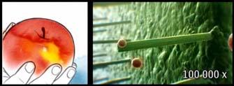
8 Stability Issues of Transparent Conducting Oxides (TCOs) for Thin-Film Photovoltaics Indium is becoming a problem NREL is a national laboratory of the U.S. Department of Energy, Office of Energy Efficiency and Renewable Energy operated by the Alliance for Sustainable Energy, LLC material From: Prof. J. Pern, NREL
9 Graphene vs. Si Charge carrier mobility cm 2 /Vs (Si: 1400 cm 2 /Vs) Charge carrier density 3 x cm -2 (Si: 1.3 x cm 3 intrinsic) Current density A/cm 2 (Si: 3x 10 5 A/cm 2 on transistor) Thermal conductivity 5000 Wm -1 K -1 (Si: 163 Wm -1 K -1 at room temp.) (heat dissipation on nanoscale is a serious issue!!!) Transparent & the strongest material known
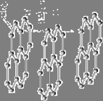

10 Carbon before1985 sp 2 Graphite sp 3 Diamond
11 The family of carbon nanostructures Fullerene Carbon nanotube Graphene 1985 H.W.Kroto, R. Smalley & R. Curl 1991 S. Iijima 2004 K. S. Novoselov & A. Geim Nobel Prize 1996 Kavli Prize 2008 Nobel Prize 2010


12 The family of carbon nanostructures Fullerene Carbon nanotube Graphene 1985 H.W.Kroto, R. Smalley & R. Curl 1991 S. Iijima 2004 K. S. Novoselov & A. Geim Nobel Prize 1996 Kavli Prize 2008 Nobel Prize 2010


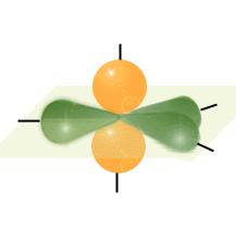
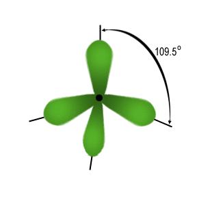
13 Structure & Electronic structure armchair zig-zag C-C bond shorter than in diamond! Wu, Y. H.; Yu, T.; Shen, Z. X. J. Appl. Phys. 2010, 108, The FIRST truly one single atom thick material! Different properties along different crystallographic directions. EXTRAORDINARY electronic structure!


14 Linear dispersion & Klein tunneling Graphene Regular material Bilayer A. H. Castro Neto et al., Rev. Mod. Phys. 2009, 81, The charge carriers cannot be confined by electrostatic barriers like in conventional semiconductors Katsnelson, M. Materials Today 2007, 10, p = 1 x cm -2 p = 3 x cm -2


15 Transparent & flexible material GR-O Before CVD Nair, R. R. et al. Science 2008, 320, After Bending graphene vs. ITO on PET Wassei, J. K.; Kaner, R. B. Materials Today 2010, 13,
 Bunch, J. S. et al, Nano Lett.")
16 Highly stretchable material, impermeable to gases AFM image Δz = 175 nm AFM linecuts in time (3 days!) Bunch, J. S. et al, Nano Lett. 8 (2008) 2458.
17 Properties & Applications Linear dispersion One atom thin High mobility High strength Unique optical properties Highly stretchable

18 Properties & Applications Linear dispersion Transistors High mobility Quantum Hall Effect & Spintronics One atom thin Membranes, ultracapacitors High strength Photovoltaics Unique optical properties Transparent & flexible conductors Composites Highly stretchable

 Chemical exfoliation")
 CNT unzipping and many")
19 Production of graphene Micromechanical cleavage Epitaxy on SiC CVD (Ni, Pt, Rh, Cu) Chemical exfoliation (G- O, oxigene removal!) CNT unzipping and many other exotic methods.

20 Production of graphene Micromechanical cleavage Epitaxy on SiC CVD (Ni, Pt, Rh, Cu) Chemical exfoliation (G- O, oxigene removal!) CNT unzipping and many other exotic methods.

21 Production of graphene Micromechanical cleavage Epitaxy on SiC CVD (Ni, Pt, Rh, Cu) Chemical exfoliation (G- O, oxigene removal!) CNT unzipping and many other exotic methods.

22 Production of graphene Micromechanical cleavage Epitaxy on SiC CVD (Ni, Pt, Rh, Cu) Chemical exfoliation (G- O, oxigene removal!) CNT unzipping and many other exotic methods.

23 Production of graphene Micromechanical cleavage Epitaxy on SiC CVD (Ni, Pt, Rh, Cu) Chemical exfoliation (G- O, oxigene removal!) CNT unzipping and many other exotic methods.


24 Roll-to-roll large size CVD graphene Bae, S. et al.,. Nature Nanotechnology 2010, 5, 574. The quality of the material is well suited for transparent conducting & flexible electrodes => market ready!


25 Grain boundaries in CVD grown graphene Liu, T.-H., et al., Carbon 2011, 49, 2306 The grain boundaries decrease the very high mobility values by times. The grain structure must be revealed for the optimization of the growth conditions. 10 μm Li, X. et al. Nano Letters 10 ( 2010) Random nucleation => many grain boundaries

26 Characterization of grain structure by AFM 1. STEP: Reveal the grain boundaries by selective oxidation (negative comparison exfoliated graphene) P. Nemes-Incze et al. Submitted to Appl. Phys. Lett


27 Characterization of grain structure by AFM 2. STEP: Analyze the grain size and the relative angle of grain boundaries by atomic resolution AFM images P. Nemes-Incze et al. Submitted to Appl. Phys. Lett

28 Application in high speed nanoelectronics NO switched off state => NO DIGITAL applications


29 The electronic structure has to be reengineered Badgap induced by confinement Graphene nanoribbons Armchair Zigzag
30 ALL GRAPHENE nanoelectronics T = 0. 3 K!!! SET 20 nm Areshkin, D. A.; White, C. T. Nano letters 2007, 7, 3253 Ponomarenko, L.. Science 2008, 320, 356-


31 STM lithography - Local modification of sample surface - Atomically precise tip positioning - Atomic resolution imaging To solve: - Control the etching process, realize the first true nanometer precision lithography
32 Graphene nanoribbons created by STM lithography L. Tapasztó et al. Nature Nanotechnology, 4, 937 (2008)


33 Graphene nanoribbons created by STM lithography L. Tapasztó et al. Nature Nanotechnology, 4, 937 (2008)


34 Atomic resolution STM imaging of GNRs 2 nm L. Tapasztó et al. Nature Nanotechnology, 4, 937 (2008)
 = W ( 2eV")

35 Electron standing waves at room temperature 1 nm ( W ) = W ( 2eV nm) W L. Tapasztó et al. Nature Nanotechnology, 4, 937 (2008) E g πhν 0
 E g = 0.")
36 STILL the t best lithographic resolution today 1 nm L. Tapasztó et al. Nature Nanotechnology, 4, 937 (2008) E g = 0.5 ev allows room temperature operation!


37 Atomically perfect zigzag edges by: Carbothermal Etching (CTE) P. Nemes-Incze et al., Nano Res. 3 (2010) 110

38 Edge orientation by STM P. Nemes-Incze et al., Nano Res. 3 (2010) 110
 110")
39 Starting point fixed by AFM indentation P. Nemes-Incze et al., Nano Res. 3 (2010) 110

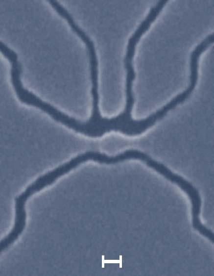
40 Nanoarchitectures: graphene nano-y Junction P. Nemes-Incze et al., Nano Res. 3 (2010) 110

 3498 Supercapacitors")
 Nature Materials 7 (2008) 966 NiO Resistive Random")
41 Further applications nd_bc_ultracapacitor_cells_and_modules.jpg Nano Letters 8 (2008) 3498 Supercapacitors (Ultracapacitors?) Nature Materials 7 (2008) 966 NiO Resistive Random Access Memory Nanocapacitor Array on Graphene ACS Nano, 2010, 4 (5), pp 2655 Memory devices
electronics http://www.crunchwear.")

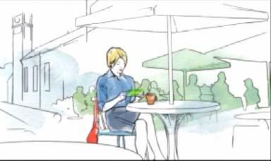
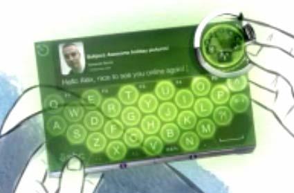
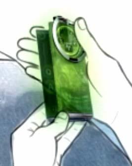
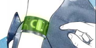
42 FLEXIBLE (Trasistors + memory + energy source) = WEARABLE (nano)electronics Augmented-realityholographic sunglasses m/vuzix-and-darpa-teamup-to-create-augmentedreality-holographicsunglasses/ Solar Soldier system to take the weight off infantry soldiers -soldier-power-system-forinfantry/18140/


43 NOKIA Let s stop here
44 Summary Graphene is the first of the family of single atom (molecule) thin materials It has many extraordinary properties It has short range application possibilities in flexible flat screens and photovoltaic devices It has long range perspectives to replace silicon in nanolectronic devices bandgap reengineering needed atomic precision nanolithograpy Flexible and wearable electronics from power source to fast logic and memory

45 Acknowledgments Funding: In Hungary OTKA-NKTH: K67793 Nanoarchitectures from nanostructures Korean-Hungarian Joint Laboratory for Nanosciences MFA: P. Nemes-Incze, G. Dobrik, P. Vancsó, G. I. Márk, Z. Vértesy, Z. E. Horváth, L. Tapasztó, KRISS: K. J. Yoo & C. Hwang

46 Graphene FLAGSHIP EU-FP7
GRAPHENE NANORIBBONS Nahid Shayesteh,
 USC Department of Physics Graduate Seminar 1 GRAPHENE NANORIBBONS Nahid Shayesteh, Outlines 2 Carbon based material Discovery and innovation of graphen Graphene nanoribbons structure Application of Graphene
Wafer-scale fabrication of graphene
 Wafer-scale fabrication of graphene Sten Vollebregt, MSc Delft University of Technology, Delft Institute of Mircosystems and Nanotechnology Delft University of Technology Challenge the future Delft University
CVD growth of Graphene. SPE ACCE presentation Carter Kittrell James M. Tour group September 9 to 11, 2014
 CVD growth of Graphene SPE ACCE presentation Carter Kittrell James M. Tour group September 9 to 11, 2014 Graphene zigzag armchair History 1500: Pencil-Is it made of lead? 1789: Graphite 1987: The first
Graphene Fundamentals and Emergent Applications
 Graphene Fundamentals and Emergent Applications Jamie H. Warner Department of Materials University of Oxford Oxford, UK Franziska Schaffel Department of Materials University of Oxford Oxford, UK Alicja
Carbon Nanomaterials: Nanotubes and Nanobuds and Graphene towards new products 2030
 Carbon Nanomaterials: Nanotubes and Nanobuds and Graphene towards new products 2030 Prof. Dr. Esko I. Kauppinen Helsinki University of Technology (TKK) Espoo, Finland Forecast Seminar February 13, 2009
Graphene films on silicon carbide (SiC) wafers supplied by Nitride Crystals, Inc.
 wafers supplied by Nitride Crystals, Inc.") 9702 Gayton Road, Suite 320, Richmond, VA 23238, USA Phone: +1 (804) 709-6696 info@nitride-crystals.com www.nitride-crystals.com Graphene films on silicon carbide (SiC) wafers supplied by Nitride Crystals,
9702 Gayton Road, Suite 320, Richmond, VA 23238, USA Phone: +1 (804) 709-6696 info@nitride-crystals.com www.nitride-crystals.com Graphene films on silicon carbide (SiC) wafers supplied by Nitride Crystals,
Overview. Carbon in all its forms. Background & Discovery Fabrication. Important properties. Summary & References. Overview of current research
 Graphene Prepared for Solid State Physics II Pr Dagotto Spring 2009 Laurene Tetard 03/23/09 Overview Carbon in all its forms Background & Discovery Fabrication Important properties Overview of current
Lectures Graphene and
 Lectures 15-16 Graphene and carbon nanotubes Graphene is atomically thin crystal of carbon which is stronger than steel but flexible, is transparent for light, and conducts electricity (gapless semiconductor).
Session V: Graphene. Matteo Bruna CAMBRIDGE UNIVERSITY DEPARTMENT OF ENGINEERING
 Session V: Graphene Matteo Bruna Graphene: Material in the Flatland Graphite Graphene Properties: Thinnest imaginable material Good(and tunable) electrical conductor Strongest ever measured Stiffest known
Nanostrukturphysik (Nanostructure Physics)
") Nanostrukturphysik (Nanostructure Physics) Prof. Yong Lei & Dr. Yang Xu Fachgebiet 3D-Nanostrukturierung, Institut für Physik Contact: yong.lei@tu-ilmenau.de; yang.xu@tu-ilmenau.de Office: Unterpoerlitzer
Nanostrukturphysik (Nanostructure Physics) Prof. Yong Lei & Dr. Yang Xu Fachgebiet 3D-Nanostrukturierung, Institut für Physik Contact: yong.lei@tu-ilmenau.de; yang.xu@tu-ilmenau.de Office: Unterpoerlitzer
Nanotechnology in Consumer Products
 Nanotechnology in Consumer Products June 17, 2015 October 31, 2014 The webinar will begin at 1pm Eastern Time Perform an audio check by going to Tools > Audio > Audio Setup Wizard Chat Box Chat Box Send
2-D Layered Materials 1
 2-D Layered Materials 1 Flatlands beyond Graphene Why the interest? 2D crystal with extraordinarily few defects Exotic electrical behaviors E = v F P (massless Dirac fermions) Efficient tunneling through
GRAPHENE NANORIBBONS Nahid Shayesteh,
 USC Department of Physics Graduate Seminar GRAPHENE NANORIBBONS Nahid Shayesteh, Outlines 2 Carbon based material Discovery and innovation of graphen Graphene nanoribbons structure and... FUNCTIONS 3 Carbon-based
1. Nanotechnology & nanomaterials -- Functional nanomaterials enabled by nanotechnologies.
 Novel Nano-Engineered Semiconductors for Possible Photon Sources and Detectors NAI-CHANG YEH Department of Physics, California Institute of Technology 1. Nanotechnology & nanomaterials -- Functional nanomaterials
Carbon nanomaterials. Gavin Lawes Wayne State University.
 Carbon nanomaterials Gavin Lawes Wayne State University glawes@wayne.edu Outline 1. Carbon structures 2. Carbon nanostructures 3. Potential applications for Carbon nanostructures Periodic table from bpc.edu
Graphene Novel Material for Nanoelectronics
 Graphene Novel Material for Nanoelectronics Shintaro Sato Naoki Harada Daiyu Kondo Mari Ohfuchi (Manuscript received May 12, 2009) Graphene is a flat monolayer of carbon atoms with a two-dimensional honeycomb
Halbleiter Prof. Yong Lei Prof. Thomas Hannappel
 Halbleiter Prof. Yong Lei Prof. Thomas Hannappel yong.lei@tu-ilmenau.de thomas.hannappel@tu-ilmenau.de http:///nanostruk/ Organic semiconductors Small-molecular materials Rubrene Pentacene Polymers PEDOT:PSS
Graphene. Tianyu Ye November 30th, 2011
 Graphene Tianyu Ye November 30th, 2011 Outline What is graphene? How to make graphene? (Exfoliation, Epitaxial, CVD) Is it graphene? (Identification methods) Transport properties; Other properties; Applications;
Nanocarbon Technology for Development of Innovative Devices
 Nanocarbon Technology for Development of Innovative Devices Shintaro Sato Daiyu Kondo Shinichi Hirose Junichi Yamaguchi Graphene, a one-atom-thick honeycomb lattice made of carbon, and a carbon nanotube,
STM and graphene. W. W. Larry Pai ( 白偉武 ) Center for condensed matter sciences, National Taiwan University NTHU, 2013/05/23
 Center for condensed matter sciences, National Taiwan University NTHU, 2013/05/23") STM and graphene W. W. Larry Pai ( 白偉武 ) Center for condensed matter sciences, National Taiwan University NTHU, 2013/05/23 Why graphene is important: It is a new form of material (two dimensional, single
STM and graphene W. W. Larry Pai ( 白偉武 ) Center for condensed matter sciences, National Taiwan University NTHU, 2013/05/23 Why graphene is important: It is a new form of material (two dimensional, single
From nanophysics research labs to cell phones. Dr. András Halbritter Department of Physics associate professor
 From nanophysics research labs to cell phones Dr. András Halbritter Department of Physics associate professor Curriculum Vitae Birth: 1976. High-school graduation: 1994. Master degree: 1999. PhD: 2003.
Grpahene Synthesis by CVD. QingkaiYu Ingram School of Engineering Texas State University at San Marcos
 Grpahene Synthesis by CVD QingkaiYu Ingram School of Engineering Texas State University at San Marcos @ Applied Nanotech Inc, July 25 th, 2011 Acknowledgement Texas State University Dr. Zhihong Liu Austin
Transparent Electrode Applications
 Transparent Electrode Applications LCD Solar Cells Touch Screen Indium Tin Oxide (ITO) Zinc Oxide (ZnO) - High conductivity - High transparency - Resistant to environmental effects - Rare material (Indium)
3-month progress Report
 3-month progress Report Graphene Devices and Circuits Supervisor Dr. P.A Childs Table of Content Abstract... 1 1. Introduction... 1 1.1 Graphene gold rush... 1 1.2 Properties of graphene... 3 1.3 Semiconductor
Graphene. L. Tetard 1,2. (Dated: April 7, 2009) 1 Oak Ridge National Laboratory, Oak Ridge, TN USA
 1 Oak Ridge National Laboratory, Oak Ridge, TN USA") Graphene L. Tetard 1,2 1 Oak Ridge National Laboratory, Oak Ridge, TN 37831-6123 USA 2 Department of Physics, University of Tennessee, Knoxville, TN 37996, USA (Dated: April 7, 2009) 1 Diamond, graphite,
Graphene L. Tetard 1,2 1 Oak Ridge National Laboratory, Oak Ridge, TN 37831-6123 USA 2 Department of Physics, University of Tennessee, Knoxville, TN 37996, USA (Dated: April 7, 2009) 1 Diamond, graphite,
Initial Stages of Growth of Organic Semiconductors on Graphene
 Initial Stages of Growth of Organic Semiconductors on Graphene Presented by: Manisha Chhikara Supervisor: Prof. Dr. Gvido Bratina University of Nova Gorica Outline Introduction to Graphene Fabrication
Nanotechnology. Yung Liou P601 Institute of Physics Academia Sinica
 Nanotechnology Yung Liou P601 yung@phys.sinica.edu.tw Institute of Physics Academia Sinica 1 1st week Definition of Nanotechnology The Interagency Subcommittee on Nanoscale Science, Engineering and Technology
Nanostrukturphysik Übung 2 (Class 3&4)
") Nanostrukturphysik Übung 2 (Class 3&4) Prof. Yong Lei & Dr. Yang Xu 2017.05.03 Fachgebiet 3D-Nanostrukturierung, Institut für Physik Contact: yong.lei@tu-ilmenau.de (3748), yang.xu@tuilmenau.de (4902)
Nanostrukturphysik Übung 2 (Class 3&4) Prof. Yong Lei & Dr. Yang Xu 2017.05.03 Fachgebiet 3D-Nanostrukturierung, Institut für Physik Contact: yong.lei@tu-ilmenau.de (3748), yang.xu@tuilmenau.de (4902)
Ultralong natural graphene nanoribbons and their electrical conductivity**
 Ultralong natural graphene nanoribbons and their electrical conductivity** By M. Moreno-Moreno, A. Castellanos-Gomez, G. Rubio-Bollinger, J. Gomez-Herrero *, N. Agraït *. [*] Prof. J. Gómez-Herrero, Prof.
The many forms of carbon
 The many forms of carbon Carbon is not only the basis of life, it also provides an enormous variety of structures for nanotechnology. This versatility is connected to the ability of carbon to form two
Supplementary Figure S1. AFM images of GraNRs grown with standard growth process. Each of these pictures show GraNRs prepared independently,
 Supplementary Figure S1. AFM images of GraNRs grown with standard growth process. Each of these pictures show GraNRs prepared independently, suggesting that the results is reproducible. Supplementary Figure
Carbon based Nanoscale Electronics
 Carbon based Nanoscale Electronics 09 02 200802 2008 ME class Outline driving force for the carbon nanomaterial electronic properties of fullerene exploration of electronic carbon nanotube gold rush of
EN2912C: Future Directions in Computing Lecture 08: Overview of Near-Term Emerging Computing Technologies
 EN2912C: Future Directions in Computing Lecture 08: Overview of Near-Term Emerging Computing Technologies Prof. Sherief Reda Division of Engineering Brown University Fall 2008 1 Near-term emerging computing
1. Introduction : 1.2 New properties:
 Nanodevices In Electronics Rakesh Kasaraneni(PID : 4672248) Department of Electrical Engineering EEL 5425 Introduction to Nanotechnology Florida International University Abstract : This paper describes
Molecular Dynamics Study of Thermal Rectification in Graphene Nanoribbons
 Molecular Dynamics Study of Thermal Rectification in Graphene Nanoribbons Jiuning Hu 1* Xiulin Ruan 2 Yong P. Chen 3# 1School of Electrical and Computer Engineering and Birck Nanotechnology Center, Purdue
SiC Graphene Suitable For Quantum Hall Resistance Metrology.
 SiC Graphene Suitable For Quantum Hall Resistance Metrology. Samuel Lara-Avila 1, Alexei Kalaboukhov 1, Sara Paolillo, Mikael Syväjärvi 3, Rositza Yakimova 3, Vladimir Fal'ko 4, Alexander Tzalenchuk 5,
Molecular Dynamics Study of Thermal Rectification in Graphene Nanoribbons
 Int J Thermophys (2012) 33:986 991 DOI 10.1007/s10765-012-1216-y Molecular Dynamics Study of Thermal Rectification in Graphene Nanoribbons Jiuning Hu Xiulin Ruan Yong P. Chen Received: 26 June 2009 / Accepted:
PHYS-E0424 Nanophysics Lecture 5: Fullerenes, Carbon Nanotubes and Graphene
 PHYS-E0424 Nanophysics Lecture 5: Fullerenes, Carbon Nanotubes and Graphene PHYS-E0424 Nanophysics Lecture 5: Carbon Nanostructures Sebastiaan van Dijken 1 SEM/TEM Recently I was operating SEM for a first
Commercial Graphene Applications: Current Research and Future Prospects
 Commercial Graphene Applications: Current Research and Future Prospects Overview History and Overview of Graphene Angstron Materials and Nanotek Instruments Applications of Graphene Thermal Management
Current Status of Graphene Transistors. Max C. Lemme
 Current Status of Graphene Transistors Max C. Lemme Department of Physics, Harvard University, 17 Oxford Street, Cambridge, MA02138, USA, lemme@fas.harvard.edu Keywords: graphene, transistor, MOSFET, mobility,
Selective etching of armchair edges in graphite
 CARBON 56 (2013) 332 338 Available at www.sciencedirect.com journal homepage: www.elsevier.com/locate/carbon Selective etching of armchair edges in graphite G. Dobrik *, L. Tapasztó, L.P. Biró Institute
Engineered Flexible Conductive Barrier Films for Advanced Energy Devices
 The 13 th Korea-U.S. Forum on Nanotechnology Engineered Flexible Conductive Barrier Films for Advanced Energy Devices Jinsung Kwak 1, Yongsu Jo 1, Soon-Dong Park 2, Na Yeon Kim 1, Se-Yang Kim 1, Zonghoon
GRAPHENE the first 2D crystal lattice
 GRAPHENE the first 2D crystal lattice dimensionality of carbon diamond, graphite GRAPHENE realized in 2004 (Novoselov, Science 306, 2004) carbon nanotubes fullerenes, buckyballs what s so special about
Carbon Nanotubes. Andrea Goldoni. Elettra- Sincrotrone Trieste S.C.p.A., s.s. 14 Km 163,5 in Area Science Park, Trieste, Italy
 Carbon Nanotubes Andrea Goldoni Elettra- Sincrotrone Trieste S.C.p.A., s.s. 14 Km 163,5 in Area Science Park, 34012 Trieste, Italy Up to 1985 the only two allotropic form of carbon were known: graphite
CHAPTER 11 Semiconductor Theory and Devices
 CHAPTER 11 Semiconductor Theory and Devices 11.1 Band Theory of Solids 11.2 Semiconductor Theory 11.3 Semiconductor Devices 11.4 Nanotechnology It is evident that many years of research by a great many
Available online at ScienceDirect. Procedia Materials Science 11 (2015 )
") Available online at www.sciencedirect.com ScienceDirect Procedia Materials Science 11 (2015 ) 407 411 5th International Biennial Conference on Ultrafine Grained and Nanostructured Materials, FGNSM15 Simulation
Available online at www.sciencedirect.com ScienceDirect Procedia Materials Science 11 (2015 ) 407 411 5th International Biennial Conference on Ultrafine Grained and Nanostructured Materials, FGNSM15 Simulation
A. Optimizing the growth conditions of large-scale graphene films
 1 A. Optimizing the growth conditions of large-scale graphene films Figure S1. Optical microscope images of graphene films transferred on 300 nm SiO 2 /Si substrates. a, Images of the graphene films grown
PHYS 3313 Section 001 Lecture #21 Monday, Nov. 26, 2012
 PHYS 3313 Section 001 Lecture #21 Monday, Nov. 26, 2012 Superconductivity Theory, The Cooper Pair Application of Superconductivity Semi-Conductor Nano-technology Graphene 1 Announcements Your presentations
Seminars in Nanosystems - I
 Seminars in Nanosystems - I Winter Semester 2011/2012 Dr. Emanuela Margapoti Emanuela.Margapoti@wsi.tum.de Dr. Gregor Koblmüller Gregor.Koblmueller@wsi.tum.de Seminar Room at ZNN 1 floor Topics of the
7. Carbon Nanotubes. 1. Overview: Global status market price 2. Types. 3. Properties. 4. Synthesis. MWNT / SWNT zig-zag / armchair / chiral
 7. Carbon Nanotubes 1. Overview: Global status market price 2. Types MWNT / SWNT zig-zag / armchair / chiral 3. Properties electrical others 4. Synthesis arc discharge / laser ablation / CVD 5. Applications
Conference Return Seminar- NANO2014,Moscow State University,Moscow,Russia Date: th July 2014
 Conference Return Seminar- NANO2014,Moscow State University,Moscow,Russia Date:13-1818 th July 2014 An electrochemical method for the synthesis of single and few layers graphene sheets for high temperature
NEM Relays Using 2-Dimensional Nanomaterials for Low Energy Contacts
 NEM Relays Using 2-Dimensional Nanomaterials for Low Energy Contacts Seunghyun Lee, Ji Cao 10/29/2013 A Science & Technology Professor H. -S. Philip Wong Electrical Engineering, Stanford University Center
2D MBE Activities in Sheffield. I. Farrer, J. Heffernan Electronic and Electrical Engineering The University of Sheffield
 2D MBE Activities in Sheffield I. Farrer, J. Heffernan Electronic and Electrical Engineering The University of Sheffield Outline Motivation Van der Waals crystals The Transition Metal Di-Chalcogenides
Exceptional ballistic transport in epigraphene. Walt de Heer Georgia Institute of Technology
 Exceptional ballistic transport in epigraphene Walt de Heer Georgia Institute of Technology Program Objective First formulated in 2001 and patented in 2003, our objective is to develop nanoelectronics
& Dirac Fermion confinement Zahra Khatibi
 Graphene & Dirac Fermion confinement Zahra Khatibi 1 Outline: What is so special about Graphene? applications What is Graphene? Structure Transport properties Dirac fermions confinement Necessity External
Chapter 1 Introduction
 Chapter 1 Introduction In our planet carbon forms the basis of all organic molecules which makes it the most important element of life. It is present in over 95% of the known chemical compounds overall
SUPPLEMENTARY INFORMATION
 SUPPLEMENTARY INFORMATION Flexible, high-performance carbon nanotube integrated circuits Dong-ming Sun, Marina Y. Timmermans, Ying Tian, Albert G. Nasibulin, Esko I. Kauppinen, Shigeru Kishimoto, Takashi
SUPPLEMENTARY INFORMATION
 SUPPLEMENTARY INFORMATION Facile Synthesis of High Quality Graphene Nanoribbons Liying Jiao, Xinran Wang, Georgi Diankov, Hailiang Wang & Hongjie Dai* Supplementary Information 1. Photograph of graphene
Evaluation of Electronic Characteristics of Double Gate Graphene Nanoribbon Field Effect Transistor for Wide Range of Temperatures
 Evaluation of Electronic Characteristics of Double Gate Graphene Nanoribbon Field Effect Transistor for Wide Range of Temperatures 1 Milad Abtin, 2 Ali Naderi 1 Department of electrical engineering, Masjed
Carbon Materials for Electronic, Environmental and Biomedical Application
 Carbon Materials for Electronic, Environmental and Biomedical Application Seong-Cheol Kim School of Chemical Engineering Yeungnam University Nanomaterials for Electronics & Biomedical Uses 1. Organic Nanomaterials
Physics and Material Science of Semiconductor Nanostructures
 Physics and Material Science of Semiconductor Nanostructures PHYS 570P Prof. Oana Malis Email: omalis@purdue.edu Course website: http://www.physics.purdue.edu/academic_programs/courses/phys570p/ 1 Course
Efficient Preparation of Large-Area Graphene Oxide Sheets for Transparent Conductive Films
 Supporting Information Efficient Preparation of Large-Area Graphene Oxide Sheets for Transparent Conductive Films Jinping Zhao, Songfeng Pei, Wencai Ren*, Libo Gao and Hui-Ming Cheng* Shenyang National
Carbon Engineering Nanocarbon Structures
 Carbon Engineering Nanocarbon Structures Diamond Fullerenes Carbon nanotubes (CNT) multiwalled (MNT) Diamond Like Carbon (DLC) Graphene Nanospheres Allotropes of Carbon Crystalline Diamond Graphite Carbon
Applications of ion beams in materials science
 Applications of ion beams in materials science J. Gyulai Research Institute for Technical Physics and Materials Science (MFA), Hung. Acad. Sci., Budapest Types of processing technologies Top-down - waste
Recap (so far) Low-Dimensional & Boundary Effects
 Low-Dimensional & Boundary Effects") Recap (so far) Ohm s & Fourier s Laws Mobility & Thermal Conductivity Heat Capacity Wiedemann-Franz Relationship Size Effects and Breakdown of Classical Laws 1 Low-Dimensional & Boundary Effects Energy
Recap (so far) Ohm s & Fourier s Laws Mobility & Thermal Conductivity Heat Capacity Wiedemann-Franz Relationship Size Effects and Breakdown of Classical Laws 1 Low-Dimensional & Boundary Effects Energy
Nanostructures. Lecture 13 OUTLINE
 Nanostructures MTX9100 Nanomaterials Lecture 13 OUTLINE -What is quantum confinement? - How can zero-dimensional materials be used? -What are one dimensional structures? -Why does graphene attract so much
Graphene transistor. Seminar I a. Mentor: doc. dr. Tomaž Rejec. April Abstract
 Graphene transistor Seminar I a Jan Srpčič Mentor: doc. dr. Tomaž Rejec April 2015 Abstract The topic of this seminar is graphene and its possible applications in the field of electronics, most notably
Supplementary Figure 1 Dark-field optical images of as prepared PMMA-assisted transferred CVD graphene films on silicon substrates (a) and the one
 and the one") Supplementary Figure 1 Dark-field optical images of as prepared PMMA-assisted transferred CVD graphene films on silicon substrates (a) and the one after PBASE monolayer growth (b). 1 Supplementary Figure
Supplementary Figure 1 Dark-field optical images of as prepared PMMA-assisted transferred CVD graphene films on silicon substrates (a) and the one after PBASE monolayer growth (b). 1 Supplementary Figure
p-n Junction of 1.95 nm Carbon Nanotube: Fabrication, Properties and Performance
 American Journal of Engineering and Applied Sciences Original Research Paper p-n Junction of 1.95 nm Carbon Nanotube: Fabrication, Properties and Performance Soheli Farhana and Mohamad Fauzan Noordin Faculty
Surface atoms/molecules of a material act as an interface to its surrounding environment;
 1 Chapter 1 Thesis Overview Surface atoms/molecules of a material act as an interface to its surrounding environment; their properties are often complicated by external adsorbates/species on the surface
Nanomaterials and their Optical Applications
 Nanomaterials and their Optical Applications Winter Semester 2012 Lecture 06 Tentative version of November 13, 2012 Check for the definitive version after the lecture rachel.grange@uni-jena.de http://www.iap.uni-jena.de/multiphoton
Low Dimensional System & Nanostructures Angel Rubio & Nerea Zabala. Carbon Nanotubes A New Era
 Low Dimensional System & Nanostructures Angel Rubio & Nerea Zabala Carbon Nanotubes A New Era By Afaf El-Sayed 2009 Outline World of Carbon - Graphite - Diamond - Fullerene Carbon Nanotubes CNTs - Discovery
Ph.D. students, postdocs, and young researchers, which need to absorb a lot of new knowledge, not taught at universities, in a rather short time.
 We have started to work in the area of graphene at the end of 2006, discovering that the fascinating Dirac equations could drive to new discoveries in solid-state physics. At that time, although the Dirac
Transport Properties of Graphene Nanoribbon Transistors on. Chemical-Vapor-Deposition Grown Wafer-Scale Graphene
 Transport Properties of Graphene Nanoribbon Transistors on Chemical-Vapor-Deposition Grown Wafer-Scale Graphene Wan Sik Hwang 1, a), Kristof Tahy 1, Xuesong Li 2, Huili (Grace) Xing 1, Alan C. Seabaugh
GRAPHENE PRODUCTION. ... towards the dream of a flatland. G. Amato, M. Piazzi. UNIVERSITÀ DEGLI STUDI DI TORINO I.N.Ri.M. - Torino
 GRAPHENE PRODUCTION... towards the dream of a flatland G. Amato, M. Piazzi UNIVERSITÀ DEGLI STUDI DI TORINO I.N.Ri.M. - Torino Turin, 21 October 2010 Outline 1 Introduction and motivations Brief review
Graphene: Plane and Simple Electrical Metrology?
 Graphene: Plane and Simple Electrical Metrology? R. E. Elmquist, F. L. Hernandez-Marquez, M. Real, T. Shen, D. B. Newell, C. J. Jacob, and G. R. Jones, Jr. National Institute of Standards and Technology,
Electronic and Photonic Applications of One- Dimensional Carbon and Silicon Nanostructures
 Electronic and Photonic Applications of One- Dimensional Carbon and Silicon Nanostructures Anupama B. Kaul Jet Propulsion Laboratory, California Institute of Technology, Pasadena, CA 91109 Ph: (818) 393-7186;
Carbon Structure Simulations using Crystal Viewer Tool
 Carbon Structure Simulations using Crystal Viewer Tool The Crystal Viewer tool in nanohub.org can be used to build three carbon nanostructures: graphene sheets, Buckminsterfullerene, Bucky balls (C 60
Graphene devices and integration: A primer on challenges
 Graphene devices and integration: A primer on challenges Archana Venugopal (TI) 8 Nov 2016 Acknowledgments: Luigi Colombo (TI) UT Dallas and UT Austin 1 Outline Where we are Issues o Contact resistance
3/10/2013. Lecture #1. How small is Nano? (A movie) What is Nanotechnology? What is Nanoelectronics? What are Emerging Devices?
 What is Nanotechnology? What is Nanoelectronics? What are Emerging Devices?") EECS 498/598: Nanocircuits and Nanoarchitectures Lecture 1: Introduction to Nanotelectronic Devices (Sept. 5) Lectures 2: ITRS Nanoelectronics Road Map (Sept 7) Lecture 3: Nanodevices; Guest Lecture by
EECS 498/598: Nanocircuits and Nanoarchitectures Lecture 1: Introduction to Nanotelectronic Devices (Sept. 5) Lectures 2: ITRS Nanoelectronics Road Map (Sept 7) Lecture 3: Nanodevices; Guest Lecture by
Manufacture of Nanostructures for Power Electronics Applications
 Manufacture of Nanostructures for Power Electronics Applications Brian Hunt and Jon Lai Etamota Corporation 2672 E. Walnut St. Pasadena, CA 91107 APEC, Palm Springs Feb. 23rd, 2010 1 Background Outline
TRANSVERSE SPIN TRANSPORT IN GRAPHENE
 International Journal of Modern Physics B Vol. 23, Nos. 12 & 13 (2009) 2641 2646 World Scientific Publishing Company TRANSVERSE SPIN TRANSPORT IN GRAPHENE TARIQ M. G. MOHIUDDIN, A. A. ZHUKOV, D. C. ELIAS,
NANO TECHNOLOGY IN POLYMER SOLAR CELLS. Mayur Padharia, Hardik Panchal, Keval Shah, *Neha Patni, Shibu.G.Pillai
 NANO TECHNOLOGY IN POLYMER SOLAR CELLS Mayur Padharia, Hardik Panchal, Keval Shah, *Neha Patni, Shibu.G.Pillai Department of Chemical Engineering, Institute of Technology, Nirma University, S. G. Highway,
ARCHITECTURE AND CAD FOR CARBON NANOMATERIAL INTEGRATED CIRCUITS SCOTT ERICK CHILSTEDT THESIS
 ARCHITECTURE AND CAD FOR CARBON NANOMATERIAL INTEGRATED CIRCUITS BY SCOTT ERICK CHILSTEDT THESIS Submitted in partial fulfillment of the requirements for the degree of Master of Science in Electrical and
EE130: Integrated Circuit Devices
 EE130: Integrated Circuit Devices (online at http://webcast.berkeley.edu) Instructor: Prof. Tsu-Jae King (tking@eecs.berkeley.edu) TA s: Marie Eyoum (meyoum@eecs.berkeley.edu) Alvaro Padilla (apadilla@eecs.berkeley.edu)
Introduction to semiconductor nanostructures. Peter Kratzer Modern Concepts in Theoretical Physics: Part II Lecture Notes
 Introduction to semiconductor nanostructures Peter Kratzer Modern Concepts in Theoretical Physics: Part II Lecture Notes What is a semiconductor? The Fermi level (chemical potential of the electrons) falls
Plastic Electronics. Joaquim Puigdollers.
 Plastic Electronics Joaquim Puigdollers Joaquim.puigdollers@upc.edu Nobel Prize Chemistry 2000 Origins Technological Interest First products.. MONOCROMATIC PHILIPS Today Future Technological interest Low
Nanostrukturphysik (Nanostructure Physics)
") Nanostrukturphysik (Nanostructure Physics) Prof. Yong Lei & Dr. Yang Xu Fachgebiet 3D-Nanostrukturierung, Institut für Physik Contact: yong.lei@tu-ilmenau.de; yang.xu@tu-ilmenau.de Office: Unterpoerlitzer
Nanostrukturphysik (Nanostructure Physics) Prof. Yong Lei & Dr. Yang Xu Fachgebiet 3D-Nanostrukturierung, Institut für Physik Contact: yong.lei@tu-ilmenau.de; yang.xu@tu-ilmenau.de Office: Unterpoerlitzer
Carbon-Based Electronics: Will there be a carbon age to follow the silicon age? Jeffrey Bokor EECS Department UC Berkeley
 Carbon-Based Electronics: Will there be a carbon age to follow the silicon age? Jeffrey Bokor EECS Department UC Berkeley jbokor@eecs.berkeley.edu Solid State Seminar 9-13-13 1 Outline Review of development
NANOTECHNOLOGY FOR ELECTRONICS AND SENSORS APPLICATIONS
 NANOTECHNOLOGY FOR ELECTRONICS AND SENSORS APPLICATIONS SMALLER FASTER MORE SENSETIVE MORE EFFICIENT NANO CONNECT SCANDINAVIA www.nano-connect.org Chalmers University of Technology DTU Halmstad University
NiCl2 Solution concentration. Etching Duration. Aspect ratio. Experiment Atmosphere Temperature. Length(µm) Width (nm) Ar:H2=9:1, 150Pa
 Width (nm) Ar:H2=9:1, 150Pa") Experiment Atmosphere Temperature #1 # 2 # 3 # 4 # 5 # 6 # 7 # 8 # 9 # 10 Ar:H2=9:1, 150Pa Ar:H2=9:1, 150Pa Ar:H2=9:1, 150Pa Ar:H2=9:1, 150Pa Ar:H2=9:1, 150Pa Ar:H2=9:1, 150Pa Ar:H2=9:1, 150Pa Ar:H2=9:1,
Experiment Atmosphere Temperature #1 # 2 # 3 # 4 # 5 # 6 # 7 # 8 # 9 # 10 Ar:H2=9:1, 150Pa Ar:H2=9:1, 150Pa Ar:H2=9:1, 150Pa Ar:H2=9:1, 150Pa Ar:H2=9:1, 150Pa Ar:H2=9:1, 150Pa Ar:H2=9:1, 150Pa Ar:H2=9:1,
Institute for Electron Microscopy and Nanoanalysis Graz Centre for Electron Microscopy
 Institute for Electron Microscopy and Nanoanalysis Graz Centre for Electron Microscopy Micromechanics Ass.Prof. Priv.-Doz. DI Dr. Harald Plank a,b a Institute of Electron Microscopy and Nanoanalysis, Graz
Electrostatics of Nanowire Transistors
 Electrostatics of Nanowire Transistors Jing Guo, Jing Wang, Eric Polizzi, Supriyo Datta and Mark Lundstrom School of Electrical and Computer Engineering Purdue University, West Lafayette, IN, 47907 ABSTRACTS
Transversal electric field effect in multilayer graphene nanoribbon
 Transversal electric field effect in multilayer graphene nanoribbon S. Bala kumar and Jing Guo a) Department of Electrical and Computer Engineering, University of Florida, Gainesville, Florida 32608, USA
Calculating Electronic Structure of Different Carbon Nanotubes and its Affect on Band Gap
 Calculating Electronic Structure of Different Carbon Nanotubes and its Affect on Band Gap 1 Rashid Nizam, 2 S. Mahdi A. Rizvi, 3 Ameer Azam 1 Centre of Excellence in Material Science, Applied Physics AMU,
Evolution of graphene growth on Cu and Ni studied by carbon isotope
 Evolution of graphene growth on Cu and Ni studied by carbon isotope labeling Xuesong Li a, Weiwei Cai a, Luigi Colombo b*, and Rodney S. Ruoff a* Large-area graphene is a new material with properties that
Part II Low dimensional carbon materials Carbon
 Part II Low dimensional carbon materials Carbon nanotubes (CNTs) and Graphene Outline Carbon nanomaterials Types of carbon nanomaterials Graphene and CNT Introduction Synthesis Specific topics Application
A BIT OF MATERIALS SCIENCE THEN PHYSICS
 GRAPHENE AND OTHER D ATOMIC CRYSTALS Andre Geim with many thanks to K. Novoselov, S. Morozov, D. Jiang, F. Schedin, I. Grigorieva, J. Meyer, M. Katsnelson A BIT OF MATERIALS SCIENCE THEN PHYSICS CARBON
Directions for simulation of beyond-cmos devices. Dmitri Nikonov, George Bourianoff, Mark Stettler
 Directions for simulation of beyond-cmos devices Dmitri Nikonov, George Bourianoff, Mark Stettler Outline Challenges and responses in nanoelectronic simulation Limits for electronic devices and motivation
Carbon nanotubes in a nutshell
 Carbon nanotubes in a nutshell What is a carbon nanotube? Start by considering graphite. sp 2 bonded carbon. Each atom connected to 3 neighbors w/ 120 degree bond angles. Hybridized π bonding across whole