Carbon Materials for Electronic, Environmental and Biomedical Application
|
|
|
- Helena Walters
- 5 years ago
- Views:
Transcription


1 Carbon Materials for Electronic, Environmental and Biomedical Application Seong-Cheol Kim School of Chemical Engineering Yeungnam University
2 Nanomaterials for Electronics & Biomedical Uses 1. Organic Nanomaterials (1) Small molecules - Self-assembled monolayers (SAMs) - Organic Semiconductors (OSCs) (2) Supramolecules - Dendrimers & Hyperbranched Polymers (3) Polymers - Block copolymers - Conjugated Polymers - Photoactive Polymers 2. Carbon Nanomaterials 3. Inorganic Nanomaterials 4. Hybrid Nanomaterials


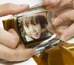

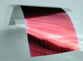


3 Future Soft Optoelectronics Touchpad electronics Touch sensor 4D electronic signature Biomedical sensor Photon sensor /imaging Nano switch Nano Materials Organic Materials Nanogenerators RAM Human-Si CMOS interfacing 2D 0D 1D + Nanorobots Smart gloves LED Active flexible electronic s Solar cell


4 Pure Carbon Nanomaterials
 (1991)")
 -")
5 Pure Carbon Nanomaterials Richard Smally Nobel Prize in Chemistry 1996 Nobel Prize in Physics 2010 (1985) (1991) (2004) Sumio Ijjima Andre Geim Konstantin Novoselov Electrical Properties - Metallic (Conductor) - Semiconductor - Insulator

6 Fullerene The most symmetrical large molecule Discovered in Nobel prize Chemistry 1996, Curl, Kroto, and Smalley C 60, also 70, 76 and facets (12 pentagons and 20 hexagons) - prototype Richard Smally (1985) ~1 nm


7 Fullerene Symmetrical shape lubricant Large surface area catalyst Hollow caging particles Ferromagnet? - polymerized C 60 - up to 220 o C

8 Fullerene Chemically stable as graphite - most reactive at pentagons Crystal by weak van der Waals force Superconductivity - K 3 C 60 : 19.2 K - RbCs 2 C 60 : 33 K Kittel, Introduction to Solid State Physics, 7the ed
 and acceptor (PCBM) are blended together to maximize the interface where exciton dissociation into electrons and holes takes place.")
9 Organic polymer solar cells (PSCs) - light weight & good mechanical properties - low cost and easy processability Figure 1: Layer structure of the polymer solar cell with approximate film thicknesses. Electron donor (P3HT) and acceptor (PCBM) are blended together to maximize the interface where exciton dissociation into electrons and holes takes place. For an efficient photocurrent, each material must provide a continuous path for electron and hole transport to the respective contact. Isolated domains can collect charges and cause recombination.
10 Carbon Nanotubes (CNTs) History 1952 L. V. Radushkevich and V. M. Lukyanovich 50 nm MWCNT Published in Soviet Journal of Physical Chemistry Cold War hurt impact of discovery Some work done before 1991 but not a hot topic The Watershed Iijima discovers MWCNT in arc burned rods Mintmire, Dunlap, and White s predict amazing electronic and physical properties 1993 Bethune and Iijima independently discover SWCNT Add Transition metal to Arc Discharge method (same method as Bucky Balls)


@(18,0)")
")
11 Carbon Nanotubes (CNTs) armchair zigzag all multiwalled Zigzag (9,0) singlewalled Rope rope

 (From Delaney et al.")
12 Classification of CNTs: ropes Ropes: bundles of SWNTs triangular array of individual SWNTs ten to several hundreds tubes tubes of different diameters and chiralities in a rope (From R. Smalley s web image gallery) (From Delaney et al., Science 1998)
 russian doll structure, several inner shells")
 (Copyright: A. Rochefort, Nano-CERCA, Univ.")
13 Classification of CNTs: many layers Multiwall nanotubes (Iijima 1991) russian doll structure, several inner shells typical radius of outermost shell > 10 nm (From Iijima, Nature 1991) (Copyright: A. Rochefort, Nano-CERCA, Univ. Montreal)
 or swiss roll (b)?")
 optimum")
14 Classification of CNTs: many layers Russian roll (a) or swiss roll (b)? Equal number of walls on either side and internal caps point towards (a) optimum distance between layers of nm
15 Carbon Nanotubes (CNTs): Physical Properties Discovered 1991, Iijima To remove the dangling bonds Roll-up vector: C h na m 1 a 2


16 Carbon Nanotubes (CNTs): Physical Properties Two symmetric structures armchair zig-zag Many chiral structures chiral

17 Carbon Nanotubes (CNTs): Physical Properties Length: typical few μm High aspect ratio: length diameter 1000 quasi 1D solid Diameter: as low as 1 nm SWCNT 1.9 nm Zheng et al. Nature Materials 3 (2004) 673.
18 Carbon Nanotubes (CNTs): Electrical Properties Electrical conductance depending on helicity C h na1 ma 2 If 2n m i, then metallic Current capacity 3 else semiconductor Carbon nanotube 1 GAmps / cm 2 Copper wire 1 MAmps / cm 2 Heat transmission Comparable to pure diamond (3320 W / m. K) Thermal stability Carbon nanotube 750 o C (in air) Metal wires in microchips o C Caging May change electrical properties sensor
19 Carbon Nanotubes (CNTs): Electrical Properties Conductivity depends on nanotubes chirality (symmetry) Armchair metallic Zigzag 1/3 metallic 2/3 semiconducting Chiral semiconducting
 High strength steel 200 GPa Tensile strength (breaking strength) Carbon nanotubes Carbon fibers High strength steel 11-63 GPa 3.")
20 Carbon Nanotubes (CNTs): Mechanical Properties Carbon nanotubes are the strongest ever known material. Young s Modulus (stiffness): Carbon nanotubes 1250 GPa Carbon fibers 425 GPa (max.) High strength steel 200 GPa Tensile strength (breaking strength) Carbon nanotubes Carbon fibers High strength steel GPa GPa ~ 2 GPa Elongation to failure : ~ % Density: Carbon nanotube (SW) gram / cm 3 Aluminium 2.7 gram / cm 3
 E r = Elastic Modulus when Searing is negligible Displacement of tube/force was measured and E r and G where")
21 Carbon Nanotubes (CNTs): Mechanical Properties SWCNT rope laid on ultra-filtration membrane AFM tip applies force to measure Shear Modulus (G) & Reduced Elastic Modulus (E r ) E r = Elastic Modulus when Searing is negligible Displacement of tube/force was measured and E r and G where calculated


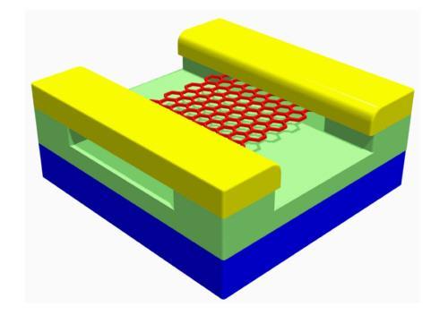
22 Overview of potential applications AFM Tip Molecular electronics Transistor FED devices Displays < Energy storage: Li-intercalation Hydrogen storage Supercapacitors < Others Composites Biomedical Catalyst support Conductive materials???

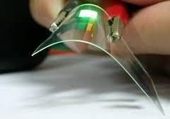
23 Application of Carbon Nanotubes (CNTs): CNT / polymer composite -Transparent electrical conductor -Thickness: nm -High flexibility Wu et al. Science 305 (2004) 1273.


24 Field-effect Nano-transistors Bachtold, Dekker et al. Science 294 (2001) 1317.


25 Chemical Sensors (a) Increase in a single SWNT conductance when 20 ppm of NO 3 are added to an Ar gas flow. (b) Same with 1% NH 3 added to the Ar gas flow Demonstration of the ability of SWNTs in detecting molecule traces in inert gases.


26 Application of Carbon Nanotubes (CNTs): Scanning Probe Microscope `New` microscopes CNT on tip of an AFM finer tip = higher resolution Small diameters of SWNTs were supposed to bring higher resolution than MWNTs due to the extremely short radius of curvature of the tube end. But commercial nanotube based tips use MWNTs for processing convenience.
:")


27 Application of Carbon Nanotubes (CNTs): Field-emission display Field Emitters phosphore Advantage of FED - High contrast level - Fast response time - Lower power consumption
")
28 Application of Carbon Nanotubes (CNTs): Yarn - CVD-grown MWCNT forest - Operation: -196 o C < T < 450 o C - Electrically conducting - Toughness comparable to Kevlar - No rupture in knot Single yarn : MPa 2-ply yarn : Mpa - High creep resistance and δ Zhang, Atkinson and Baughman, Science 306 (2004) 1358.


29 Application of Carbon Nanotubes (CNTs): Fuel Cell: Hydrogen Storage Aim: 5-7 wt% H 2 SWCNT - Dillon et al. (1997) : 8 wt% (questionable) - Tarasov et al. (2003): 2.4 wt% reversible, 25 bar H 2, -150 o C. Carbon Cones - Mealand & Skjeltorp, (2001) US Patent 6,290,753 Eldrid Svåsand, IFE Kjeller


30 Application of Carbon Nanotubes (CNTs): Fuel Cell: Hydrogen Storage CNTs as catalyst carrier for DMFC - Electrodes larger surface area, higher conductivity and excellent mechanical properties MWNTs researched for both cathode and anode: more efficient than conventional Pt-VulcanXC72R system Karl-Winnacker-Institute of Dechema e.v. in cooperation with the MPI for Solid State Research and the ICVT Institute of the University of Stuttgart are working on a SWNT-DMFC-Anode
 Cathode (Reduction) : Li 1-x Mn 2 O 4 (s) + xli + + xe LiMn 2 O 4 (s) Net")

31 Charge Storage Battery & Capacitor Anode (Oxidation) : Li x C 6 (s) xli + + xe + C 6 (s) Cathode (Reduction) : Li 1-x Mn 2 O 4 (s) + xli + + xe LiMn 2 O 4 (s) Net Rxn: Li x C 6 (s) + Li 1-x Mn 2 O 4 (s) LiMn 2 O 4 (s) + C 6 (s) E 전지 = 3.7 V J. Fischer, Matt Ray/EHP MIT/Riccardo Signorelli Lithium Ion Batteries Ultra Capacitors
: Nanomaterials in Water")
32 Application of Carbon Nanotubes (CNTs): Nanomaterials in Water Filtration


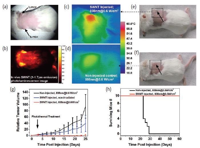
33 Modification of CNT for medical application Materials today 2011, 14,
34

")
35 Graphene (The First Nanocarbon) - Graphene is a one-atom-thick planar sheet of sp 2 -bonded carbon atoms that are densely packed in a honeycomb crystal lattice - The name graphene comes from graphite + -ene = graphene Nobel Prize in Physics 2010 (2004) Andre Geim Konstantin Novoselov High resolution transmission electron microscope images (TEM) of graphene

36 Graphene: Electrical Properties

 - Monolayer graphene absorbs πα 2.3% of white light (97.")
37 Graphene: Mechanical & Optical Properties - High Young s modulus (~1,100 Gpa) - High fracture strength (125 Gpa) - Graphene is as the strongest material ever measured, some 200 times stronger than structural steel A representation of a diamond tip with a two nanometer radius indenting into a single atomic sheet of graphene (Science, 321 (5887): 385) - Monolayer graphene absorbs πα 2.3% of white light (97.7 % transmittance), where α is the fine-structure constant.
 Preparation methods Top-down approach (From graphite) - Micromechanical exfoliation of graphite (Scotch tape or peel-off method) - Creation of colloidal suspensions from graphite oxide or graphite")
38 Graphene (How to get?) Preparation methods Top-down approach (From graphite) - Micromechanical exfoliation of graphite (Scotch tape or peel-off method) - Creation of colloidal suspensions from graphite oxide or graphite intercalation compounds (GICs) Bottom up approach (from carbon precursors) - By chemical vapor deposition (CVD) of hydrocarbon (Cu or Ni) - By epitaxial growth on electrically insulating surfaces such as SiC - By epitaxial growth on metal surfaces


39 Graphene : Top-down approach Mechanically Chemically Peel-off method Graphene


40 Graphene : Bottom-up approach Chemical Vapor Deposition Graphene

41 Chemical Modification of Graphenes Chem. Soc. Rev., 2015, 44,


42 Graphene: Application Integrated circuit Transparent electrode Transistor & Memory Solar Cell OLED B.H. Hong, Nat. Nanotechnol. 2010, 5, 574.


43 Application of Carbon Nanomaterials in Water Filtration Biofouling of membranes
44


45 Water desalination using nanoporous single-layer graphene Nature Nanotechnology 2015, 10, Porous silicone Water flow: 10 6 g/m 2 s at 40 o C ~ 3 H 2 O/pore pico-sec


46 Drug Delivery & Photo-thermal Therapy Using Graphene Oxide Materials today 2011, 14,

47 Thank you everyone You can see it as much as you know it!
Carbon nanomaterials. Gavin Lawes Wayne State University.
 Carbon nanomaterials Gavin Lawes Wayne State University glawes@wayne.edu Outline 1. Carbon structures 2. Carbon nanostructures 3. Potential applications for Carbon nanostructures Periodic table from bpc.edu
Nanotechnology in Consumer Products
 Nanotechnology in Consumer Products June 17, 2015 October 31, 2014 The webinar will begin at 1pm Eastern Time Perform an audio check by going to Tools > Audio > Audio Setup Wizard Chat Box Chat Box Send
Introduction to Nanotechnology Chapter 5 Carbon Nanostructures Lecture 1
 Introduction to Nanotechnology Chapter 5 Carbon Nanostructures Lecture 1 ChiiDong Chen Institute of Physics, Academia Sinica chiidong@phys.sinica.edu.tw 02 27896766 Section 5.2.1 Nature of the Carbon Bond
Lectures Graphene and
 Lectures 15-16 Graphene and carbon nanotubes Graphene is atomically thin crystal of carbon which is stronger than steel but flexible, is transparent for light, and conducts electricity (gapless semiconductor).
Halbleiter Prof. Yong Lei Prof. Thomas Hannappel
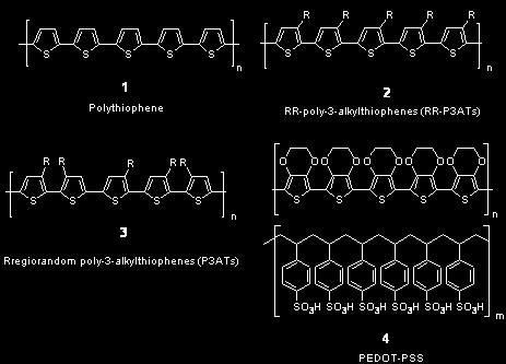
 Halbleiter Prof. Yong Lei Prof. Thomas Hannappel yong.lei@tu-ilmenau.de thomas.hannappel@tu-ilmenau.de http:///nanostruk/ Organic semiconductors Small-molecular materials Rubrene Pentacene Polymers PEDOT:PSS
Nanomaterials and their Optical Applications
 Nanomaterials and their Optical Applications Winter Semester 2012 Lecture 06 Tentative version of November 13, 2012 Check for the definitive version after the lecture rachel.grange@uni-jena.de http://www.iap.uni-jena.de/multiphoton
Graphene films on silicon carbide (SiC) wafers supplied by Nitride Crystals, Inc.
 wafers supplied by Nitride Crystals, Inc.") 9702 Gayton Road, Suite 320, Richmond, VA 23238, USA Phone: +1 (804) 709-6696 info@nitride-crystals.com www.nitride-crystals.com Graphene films on silicon carbide (SiC) wafers supplied by Nitride Crystals,
9702 Gayton Road, Suite 320, Richmond, VA 23238, USA Phone: +1 (804) 709-6696 info@nitride-crystals.com www.nitride-crystals.com Graphene films on silicon carbide (SiC) wafers supplied by Nitride Crystals,
Nanostrukturphysik (Nanostructure Physics)
") Nanostrukturphysik (Nanostructure Physics) Prof. Yong Lei & Dr. Yang Xu Fachgebiet 3D-Nanostrukturierung, Institut für Physik Contact: yong.lei@tu-ilmenau.de; yang.xu@tu-ilmenau.de Office: Unterpoerlitzer
Nanostrukturphysik (Nanostructure Physics) Prof. Yong Lei & Dr. Yang Xu Fachgebiet 3D-Nanostrukturierung, Institut für Physik Contact: yong.lei@tu-ilmenau.de; yang.xu@tu-ilmenau.de Office: Unterpoerlitzer
Carbon Nanotubes. Andrea Goldoni. Elettra- Sincrotrone Trieste S.C.p.A., s.s. 14 Km 163,5 in Area Science Park, Trieste, Italy
 Carbon Nanotubes Andrea Goldoni Elettra- Sincrotrone Trieste S.C.p.A., s.s. 14 Km 163,5 in Area Science Park, 34012 Trieste, Italy Up to 1985 the only two allotropic form of carbon were known: graphite
Carbon Nanomaterials: Nanotubes and Nanobuds and Graphene towards new products 2030
 Carbon Nanomaterials: Nanotubes and Nanobuds and Graphene towards new products 2030 Prof. Dr. Esko I. Kauppinen Helsinki University of Technology (TKK) Espoo, Finland Forecast Seminar February 13, 2009
Carbon Nanotubes. Seminar report. Submitted in partial fulfillment of the requirement for the award of degree of Mechanical.
 A Seminar report On Carbon Nanotubes Submitted in partial fulfillment of the requirement for the award of degree of Mechanical SUBMITTED TO: SUBMITTED BY: www.studymafia.org www.studymafia.org Preface
CVD growth of Graphene. SPE ACCE presentation Carter Kittrell James M. Tour group September 9 to 11, 2014
 CVD growth of Graphene SPE ACCE presentation Carter Kittrell James M. Tour group September 9 to 11, 2014 Graphene zigzag armchair History 1500: Pencil-Is it made of lead? 1789: Graphite 1987: The first
Low Dimensional System & Nanostructures Angel Rubio & Nerea Zabala. Carbon Nanotubes A New Era
 Low Dimensional System & Nanostructures Angel Rubio & Nerea Zabala Carbon Nanotubes A New Era By Afaf El-Sayed 2009 Outline World of Carbon - Graphite - Diamond - Fullerene Carbon Nanotubes CNTs - Discovery
Initial Stages of Growth of Organic Semiconductors on Graphene
 Initial Stages of Growth of Organic Semiconductors on Graphene Presented by: Manisha Chhikara Supervisor: Prof. Dr. Gvido Bratina University of Nova Gorica Outline Introduction to Graphene Fabrication
In today s lecture, we will cover:
 In today s lecture, we will cover: Metal and Metal oxide Nanoparticles Semiconductor Nanocrystals Carbon Nanotubes 1 Week 2: Nanoparticles Goals for this section Develop an understanding of the physical
7. Carbon Nanotubes. 1. Overview: Global status market price 2. Types. 3. Properties. 4. Synthesis. MWNT / SWNT zig-zag / armchair / chiral
 7. Carbon Nanotubes 1. Overview: Global status market price 2. Types MWNT / SWNT zig-zag / armchair / chiral 3. Properties electrical others 4. Synthesis arc discharge / laser ablation / CVD 5. Applications
Nanotechnology 5 th lecture
 Nanotechnology 5 th lecture (c) http://www.nccr-nano.org/nccr_data/ gallery/gallery_01/gallery_01_03/pics_06/ internet/nanotube_spiral.jpg Plan for today: http://www.nccr-nano.org/nccr_data/gallery/ gallery_01/gallery_01_03/pics_04/internet/
Carbon Structure Simulations using Crystal Viewer Tool
 Carbon Structure Simulations using Crystal Viewer Tool The Crystal Viewer tool in nanohub.org can be used to build three carbon nanostructures: graphene sheets, Buckminsterfullerene, Bucky balls (C 60
Carbon Nanotubes Activity Guide
 Carbon Nanotubes Activity Guide Quick Reference Activity Guide Activity Materials chicken wire models of different nanotube types description pages for counting schemes solid models for graphite and diamond
Synthesis of nanotubes. Ewelina Broda
 Synthesis of nanotubes Ewelina Broda Presentation Overview 1. Introduction 2. History 3. Types and structures 4. Properties 5. Synthesis 6. Applications 7. References Allotropes of Elemental Carbon History
Chapter 12: Structures & Properties of Ceramics
 Chapter 12: Structures & Properties of Ceramics ISSUES TO ADDRESS... How do the crystal structures of ceramic materials differ from those for metals? How do point defects in ceramics differ from those
Carbon Engineering Nanocarbon Structures
 Carbon Engineering Nanocarbon Structures Diamond Fullerenes Carbon nanotubes (CNT) multiwalled (MNT) Diamond Like Carbon (DLC) Graphene Nanospheres Allotropes of Carbon Crystalline Diamond Graphite Carbon
Carbon Nanotubes (CNTs)
") Carbon Nanotubes (s) Seminar: Quantendynamik in mesoskopischen Systemen Florian Figge Fakultät für Physik Albert-Ludwigs-Universität Freiburg July 7th, 2010 F. Figge (University of Freiburg) Carbon Nanotubes
Carbon Nanotubes (s) Seminar: Quantendynamik in mesoskopischen Systemen Florian Figge Fakultät für Physik Albert-Ludwigs-Universität Freiburg July 7th, 2010 F. Figge (University of Freiburg) Carbon Nanotubes
2 Symmetry. 2.1 Structure of carbon nanotubes
 2 Symmetry Carbon nanotubes are hollow cylinders of graphite sheets. They can be viewed as single molecules, regarding their small size ( nm in diameter and µm length), or as quasi-one dimensional crystals
STM and graphene. W. W. Larry Pai ( 白偉武 ) Center for condensed matter sciences, National Taiwan University NTHU, 2013/05/23
 Center for condensed matter sciences, National Taiwan University NTHU, 2013/05/23") STM and graphene W. W. Larry Pai ( 白偉武 ) Center for condensed matter sciences, National Taiwan University NTHU, 2013/05/23 Why graphene is important: It is a new form of material (two dimensional, single
STM and graphene W. W. Larry Pai ( 白偉武 ) Center for condensed matter sciences, National Taiwan University NTHU, 2013/05/23 Why graphene is important: It is a new form of material (two dimensional, single
The many forms of carbon
 The many forms of carbon Carbon is not only the basis of life, it also provides an enormous variety of structures for nanotechnology. This versatility is connected to the ability of carbon to form two
Graphene. Tianyu Ye November 30th, 2011
 Graphene Tianyu Ye November 30th, 2011 Outline What is graphene? How to make graphene? (Exfoliation, Epitaxial, CVD) Is it graphene? (Identification methods) Transport properties; Other properties; Applications;
Wafer-scale fabrication of graphene
 Wafer-scale fabrication of graphene Sten Vollebregt, MSc Delft University of Technology, Delft Institute of Mircosystems and Nanotechnology Delft University of Technology Challenge the future Delft University
CARBON NANOTUBES: PYSICAL PROPERTIES & APPLICATIONS
 REPORT TITLE CARBON NANOTUBES: PYSICAL PROPERTIES & APPLICATIONS COURSE NAME: 01NUWKI CHEMISTRY-PHYSICS OF MATERIALS FOR NANOTECHNOLOGY SUBMITTED TO: PROF. GARRONE EDOARDO SUBMITTED BY: NADIA PARVEEN MATRICULATION
Ali Ahmadpour. Fullerenes. Ali Ahmadpour. Department of Chemical Engineering Faculty of Engineering Ferdowsi University of Mashhad
 Ali Ahmadpour Fullerenes Ali Ahmadpour Department of Chemical Engineering Faculty of Engineering Ferdowsi University of Mashhad 2014 World of Carbon Materials 2 Fullerenes 1985 Robert F. Curl Jr. Richard
Carbon nanotubes in a nutshell. Graphite band structure. What is a carbon nanotube? Start by considering graphite.
 Carbon nanotubes in a nutshell What is a carbon nanotube? Start by considering graphite. sp 2 bonded carbon. Each atom connected to 3 neighbors w/ 120 degree bond angles. Hybridized π bonding across whole
Nanostrukturphysik. Prof. Yong Lei & Dr. Yang Xu Fachgebiet 3D-Nanostrukturierung, Institut für Physik
 Nanostrukturphysik Prof. Yong Lei & Dr. Yang Xu Fachgebiet 3D-Nanostrukturierung, Institut für Physik Contact: yong.lei@tu-ilmenau.de (3748), yang.xu@tuilmenau.de (4902) Office: Gebäude V202, Unterpörlitzer
Carbon nanotubes and Graphene
 16 October, 2008 Solid State Physics Seminar Main points 1 History and discovery of Graphene and Carbon nanotubes 2 Tight-binding approximation Dynamics of electrons near the Dirac-points 3 Properties
Graphene: the Route from Touch Screens to Digital Nanoelectronics
 Graphene: the Route from Touch Screens to Digital Nanoelectronics László Péter Biró Research Institute for Technical Physics & Materials Science, Budapest, Hungary http://www.nanotechnology.hu/ Human History
Nanostrukturphysik Übung 2 (Class 3&4)
") Nanostrukturphysik Übung 2 (Class 3&4) Prof. Yong Lei & Dr. Yang Xu 2017.05.03 Fachgebiet 3D-Nanostrukturierung, Institut für Physik Contact: yong.lei@tu-ilmenau.de (3748), yang.xu@tuilmenau.de (4902)
Nanostrukturphysik Übung 2 (Class 3&4) Prof. Yong Lei & Dr. Yang Xu 2017.05.03 Fachgebiet 3D-Nanostrukturierung, Institut für Physik Contact: yong.lei@tu-ilmenau.de (3748), yang.xu@tuilmenau.de (4902)
Carbon Nanotube: The Inside Story
 Krasnoyarsk: 24 th August, 2009 Carbon Nanotube: The Inside Story Review written for Journal of Nanoscience and Nanotechnology Yoshinori ANDO Dean of Faculty of Science and Technology, Meijo University
SWCNTs Single Wall Carbon Nanotubes
 Carbon Nanotubes - CNTs 1 SWCNTs Single Wall Carbon Nanotubes 2 Carbon Nanotubes - Growth 3 Carbon Nanotubes Building Principles 4 Carbon Nanotubes Building Principle 5 Carbon Nanotubes Building Principle
per unit cell Motif: Re at (0, 0, 0); 3O at ( 1 / 2, 0), (0, 0, 1 / 2 ) Re: 6 (octahedral coordination) O: 2 (linear coordination) ReO 6
; 3O at ( 1 / 2, 0), (0, 0, 1 / 2 ) Re: 6 (octahedral coordination) O: 2 (linear coordination) ReO 6") Lattice: Primitive Cubic 1ReO 3 per unit cell Motif: Re at (0, 0, 0); 3O at ( 1 / 2, 0, 0), (0, 1 / 2, 0), (0, 0, 1 / 2 ) Re: 6 (octahedral coordination) O: 2 (linear coordination) ReO 6 octahedra share
Lattice: Primitive Cubic 1ReO 3 per unit cell Motif: Re at (0, 0, 0); 3O at ( 1 / 2, 0, 0), (0, 1 / 2, 0), (0, 0, 1 / 2 ) Re: 6 (octahedral coordination) O: 2 (linear coordination) ReO 6 octahedra share
What are Carbon Nanotubes? What are they good for? Why are we interested in them?
 Growth and Properties of Multiwalled Carbon Nanotubes What are Carbon Nanotubes? What are they good for? Why are we interested in them? - Interconnects of the future? - our vision Where do we stand - our
Nanoscience & Nanotechnology-II What is happening at a very, very small length scale?
 Nanoscience & Nanotechnology-II What is happening at a very, very small length scale? Plan of the talk Fullerenes Graphene Carbon Nanotubes Properties Fullerenes The most symmetrical large molecule Discovered
Overview. Carbon in all its forms. Background & Discovery Fabrication. Important properties. Summary & References. Overview of current research
 Graphene Prepared for Solid State Physics II Pr Dagotto Spring 2009 Laurene Tetard 03/23/09 Overview Carbon in all its forms Background & Discovery Fabrication Important properties Overview of current
Introduction to Nanotechnology Chapter 5 Carbon Nanostructures Lecture 1
 Introduction to Nanotechnology Chapter 5 Carbon Nanostructures Lecture 1 ChiiDong Chen Institute of Physics, Academia Sinica chiidong@phys.sinica.edu.tw 02 27896766 Carbon contains 6 electrons: (1s) 2,
Car bo n Na no-t ube s: An Ov er view BY ARUNDUBEY ROLL NO. 0905EC ELEX. & COMM. DPTT. I. T. M., GWALIOR
 Car bo n Na no-t ube s: An Ov er view BY ARUNDUBEY ROLL NO. 0905EC071033 ELEX. & COMM. DPTT. I. T. M., GWALIOR Pre se nta tion O ve rvie w Definition History Properties Current Application Manufacturing
Graphene and Carbon Nanotubes
 Graphene and Carbon Nanotubes 1 atom thick films of graphite atomic chicken wire Novoselov et al - Science 306, 666 (004) 100μm Geim s group at Manchester Novoselov et al - Nature 438, 197 (005) Kim-Stormer
Carbon Nanotube: Property, application and ultrafast optical spectroscopy
 Carbon Nanotube: Property, application and ultrafast optical spectroscopy Yijing Fu 1, Qing Yu 1 Institute of Optics, University of Rochester Department of Electrical engineering, University of Rochester
Carbon Nanotubes in Interconnect Applications
 Carbon Nanotubes in Interconnect Applications Page 1 What are Carbon Nanotubes? What are they good for? Why are we interested in them? - Interconnects of the future? Comparison of electrical properties
The Young s Modulus of Single-Walled Carbon Nanotubes
 The Young s Modulus of Single-Walled Carbon Nanotubes Douglas Vodnik Faculty Advisor: Dr. Kevin Crosby Department of Physics, Carthage College, Kenosha, WI Abstract A new numerical method for calculating
Calculating Electronic Structure of Different Carbon Nanotubes and its Affect on Band Gap
 Calculating Electronic Structure of Different Carbon Nanotubes and its Affect on Band Gap 1 Rashid Nizam, 2 S. Mahdi A. Rizvi, 3 Ameer Azam 1 Centre of Excellence in Material Science, Applied Physics AMU,
Carbon Nanomaterials
 Carbon Nanomaterials STM Image 7 nm AFM Image Fullerenes C 60 was established by mass spectrographic analysis by Kroto and Smalley in 1985 C 60 is called a buckminsterfullerene or buckyball due to resemblance
Carbon nanotubes in a nutshell
 Carbon nanotubes in a nutshell What is a carbon nanotube? Start by considering graphite. sp 2 bonded carbon. Each atom connected to 3 neighbors w/ 120 degree bond angles. Hybridized π bonding across whole
The World of Carbon Nanotubes
 The World of Carbon Nanotubes Carbon Nanotubes Presentation by Jan Felix Eschermann at JASS05 from March 31st to April 9th, 2005 1 Outline Introduction Physical Properties Manufacturing Techniques Applications
Quantized Electrical Conductance of Carbon nanotubes(cnts)
") Quantized Electrical Conductance of Carbon nanotubes(cnts) By Boxiao Chen PH 464: Applied Optics Instructor: Andres L arosa Abstract One of the main factors that impacts the efficiency of solar cells is
Quantized Electrical Conductance of Carbon nanotubes(cnts) By Boxiao Chen PH 464: Applied Optics Instructor: Andres L arosa Abstract One of the main factors that impacts the efficiency of solar cells is
DocumentToPDF trial version, to remove this mark, please register this software.
 PAPER PRESENTATION ON Carbon Nanotube - Based Nonvolatile Random Access Memory AUTHORS M SIVARAM PRASAD Sivaram.443@gmail.com B N V PAVAN KUMAR pavankumar.bnv@gmail.com 1 Carbon Nanotube- Based Nonvolatile
Imaging Carbon materials with correlative Raman-SEM microscopy. Introduction. Raman, SEM and FIB within one chamber. Diamond.
 Imaging Carbon materials with correlative Raman-SEM microscopy Application Example Carbon materials are widely used in many industries for their exceptional properties. Electric conductance, light weight,
Chemistry 1000 Lecture 22: Group 14 and Boron. Marc R. Roussel
 Chemistry 1000 Lecture 22: Group 14 and Boron Marc R. Roussel Group 14 In this group again, we see a full range of nonmetallic to metallic behavior: C is a nonmetal. Si and Ge are metalloids. Sn and Pb
Chapter 1 Introduction
 Chapter 1 Introduction In our planet carbon forms the basis of all organic molecules which makes it the most important element of life. It is present in over 95% of the known chemical compounds overall
Chapter 1: Introduction of Carbon Nanotubes: Properties, Synthesis, Characterization and Applications
 Chapter 1: Introduction of Carbon Nanotubes: Properties, Synthesis, Characterization and Applications 1.1. Background 1.2. Introduction of carbon and their allotropes 1.3. Carbon nanotubes (CNTs) 1.4.
NANOSCIENCE AND NANOTECHNOLOGY
 NANOSCIENCE AND NANOTECHNOLOGY Yuehe Lin WHAT IS NANOTECHNOLOGY Nanotechnology is the understanding and control of matter at dimensions of roughly 1 to 100 nanometers, where unique phenomena enable novel
Lecture 12 February 3, 2014 Formation bucky balls, bucky tubes
 Lecture 12 February 3, 2014 Formation bucky balls, bucky tubes Nature of the Chemical Bond with applications to catalysis, materials science, nanotechnology, surface science, bioinorganic chemistry, and
Nano-1. Nanoscience I: Hard nanostructures. Kai Nordlund Faculty of Science Department of Physics Division of Materials Physics
 Nanoscience I: Hard nanostructures Kai Nordlund 10.10.2010 Faculty of Science Department of Physics Division of Materials Physics Contents Carbon nanostructures Background Graphene Fullerenes Nanotubes
EN2912C: Future Directions in Computing Lecture 08: Overview of Near-Term Emerging Computing Technologies
 EN2912C: Future Directions in Computing Lecture 08: Overview of Near-Term Emerging Computing Technologies Prof. Sherief Reda Division of Engineering Brown University Fall 2008 1 Near-term emerging computing
Graphene Novel Material for Nanoelectronics
 Graphene Novel Material for Nanoelectronics Shintaro Sato Naoki Harada Daiyu Kondo Mari Ohfuchi (Manuscript received May 12, 2009) Graphene is a flat monolayer of carbon atoms with a two-dimensional honeycomb
PHYS-E0424 Nanophysics Lecture 5: Fullerenes, Carbon Nanotubes and Graphene
 PHYS-E0424 Nanophysics Lecture 5: Fullerenes, Carbon Nanotubes and Graphene PHYS-E0424 Nanophysics Lecture 5: Carbon Nanostructures Sebastiaan van Dijken 1 SEM/TEM Recently I was operating SEM for a first
Seminars in Nanosystems - I
 Seminars in Nanosystems - I Winter Semester 2011/2012 Dr. Emanuela Margapoti Emanuela.Margapoti@wsi.tum.de Dr. Gregor Koblmüller Gregor.Koblmueller@wsi.tum.de Seminar Room at ZNN 1 floor Topics of the
NANO TECHNOLOGY IN POLYMER SOLAR CELLS. Mayur Padharia, Hardik Panchal, Keval Shah, *Neha Patni, Shibu.G.Pillai
 NANO TECHNOLOGY IN POLYMER SOLAR CELLS Mayur Padharia, Hardik Panchal, Keval Shah, *Neha Patni, Shibu.G.Pillai Department of Chemical Engineering, Institute of Technology, Nirma University, S. G. Highway,
FUTURISTIC MATERIALS BASED ON CARBON NANOTUBES FOR DEFENCE APPICATIONS A CASE STUDY
 FUTURISTIC MATERIALS BASED ON CARBON NANOTUBES FOR DEFENCE APPICATIONS A CASE STUDY Abrar Shaik 1 and Revanasiddappa 2* 1 Department of Mechanical Engineering, 2 Department of Engineering Chemistry, Hosur
Novel Dispersion and Self-Assembly
 Novel Dispersion and Self-Assembly of Carbon Nanotubes Mohammad F. Islam 100g Department of Chemical Engineering and Department of Materials Science & Engineering Funding Agencies http://islamgroup.cheme.cmu.edu
Conference Return Seminar- NANO2014,Moscow State University,Moscow,Russia Date: th July 2014
 Conference Return Seminar- NANO2014,Moscow State University,Moscow,Russia Date:13-1818 th July 2014 An electrochemical method for the synthesis of single and few layers graphene sheets for high temperature
Nanotechnology. Yung Liou P601 Institute of Physics Academia Sinica
 Nanotechnology Yung Liou P601 yung@phys.sinica.edu.tw Institute of Physics Academia Sinica 1 1st week Definition of Nanotechnology The Interagency Subcommittee on Nanoscale Science, Engineering and Technology
Nanostructures. Lecture 13 OUTLINE
 Nanostructures MTX9100 Nanomaterials Lecture 13 OUTLINE -What is quantum confinement? - How can zero-dimensional materials be used? -What are one dimensional structures? -Why does graphene attract so much
Carbon 1 of 19 Boardworks Ltd 2016
 Carbon 1 of 19 Boardworks Ltd 2016 Carbon 2 of 19 Boardworks Ltd 2016 The carbon atom 3 of 19 Boardworks Ltd 2016 Carbon is a non-metallic element found in group 4 of the periodic table. It has 6 electrons,
Electrical and Optical Properties. H.Hofmann
 Introduction to Nanomaterials Electrical and Optical Properties H.Hofmann Electrical Properties Ohm: G= σw/l where is the length of the conductor, measured in meters [m], A is the cross-section area of
Graphene Fundamentals and Emergent Applications
 Graphene Fundamentals and Emergent Applications Jamie H. Warner Department of Materials University of Oxford Oxford, UK Franziska Schaffel Department of Materials University of Oxford Oxford, UK Alicja
Graphene FETs EE439 FINAL PROJECT. Yiwen Meng Su Ai
 Graphene FETs EE439 FINAL PROJECT Yiwen Meng Su Ai Introduction What is Graphene? An atomic-scale honeycomb lattice made of carbon atoms Before 2004, Hypothetical Carbon Structure Until 2004, physicists
Solutions for Assignment-8
 Solutions for Assignment-8 Q1. The process of adding impurities to a pure semiconductor is called: [1] (a) Mixing (b) Doping (c) Diffusing (d) None of the above In semiconductor production, doping intentionally
Chapter 3. The structure of crystalline solids 3.1. Crystal structures
 Chapter 3. The structure of crystalline solids 3.1. Crystal structures 3.1.1. Fundamental concepts 3.1.2. Unit cells 3.1.3. Metallic crystal structures 3.1.4. Ceramic crystal structures 3.1.5. Silicate
For more information, please contact: or +1 (302)
") Introduction Graphene Raman Analyzer: Carbon Nanomaterials Characterization Dawn Yang and Kristen Frano B&W Tek Carbon nanomaterials constitute a variety of carbon allotropes including graphene, graphene
Introduction Graphene Raman Analyzer: Carbon Nanomaterials Characterization Dawn Yang and Kristen Frano B&W Tek Carbon nanomaterials constitute a variety of carbon allotropes including graphene, graphene
Functionalized Carbon Nanotubes a key to nanotechnology?
 1 27th Max Born Symposium Multiscale Modeling of Real Materials Wroclaw, Sep 19, 2010 Functionalized Carbon Nanotubes a key to nanotechnology? Karolina Milowska, Magda Birowska & Jacek A. Majewski Faculty
Grpahene Synthesis by CVD. QingkaiYu Ingram School of Engineering Texas State University at San Marcos
 Grpahene Synthesis by CVD QingkaiYu Ingram School of Engineering Texas State University at San Marcos @ Applied Nanotech Inc, July 25 th, 2011 Acknowledgement Texas State University Dr. Zhihong Liu Austin
Observation and modeling of single-wall carbon nanotube bend junctions
 PHYSICAL REVIEW B VOLUME 57, NUMBER 23 15 JUNE 1998-I Observation and modeling of single-wall carbon nanotube bend junctions Jie Han, M. P. Anantram, and R. L. Jaffe NASA Ames Research Center, Moffett
Carbon based Nanoscale Electronics
 Carbon based Nanoscale Electronics 09 02 200802 2008 ME class Outline driving force for the carbon nanomaterial electronic properties of fullerene exploration of electronic carbon nanotube gold rush of
Chemistry 1000 Lecture 24: Group 14 and Boron
 Chemistry 1000 Lecture 24: Group 14 and Boron Marc R. Roussel November 2, 2018 Marc R. Roussel Group 14 and Boron November 2, 2018 1 / 17 Group 14 In this group again, we see a full range of nonmetallic
Why are we so excited about carbon nanostructures? Mildred Dresselhaus Massachusetts Institute of Technology Cambridge, MA
 Why are we so excited about carbon nanostructures? Mildred Dresselhaus Massachusetts Institute of Technology Cambridge, MA Conference for Undergraduate Women in Physics at Yale January 18, 2009 Why are
Nanomaterials and their Optical Applications
 Nanomaterials and their Optical Applications Winter Semester 2013 Lecture 06 rachel.grange@uni-jena.de http://www.iap.uni-jena.de/multiphoton Outline: Organic nanomaterials for optics 2 1. Organic quantum-confined
Transparent Electrode Applications
 Transparent Electrode Applications LCD Solar Cells Touch Screen Indium Tin Oxide (ITO) Zinc Oxide (ZnO) - High conductivity - High transparency - Resistant to environmental effects - Rare material (Indium)
1. Nanotechnology & nanomaterials -- Functional nanomaterials enabled by nanotechnologies.
 Novel Nano-Engineered Semiconductors for Possible Photon Sources and Detectors NAI-CHANG YEH Department of Physics, California Institute of Technology 1. Nanotechnology & nanomaterials -- Functional nanomaterials
Session V: Graphene. Matteo Bruna CAMBRIDGE UNIVERSITY DEPARTMENT OF ENGINEERING
 Session V: Graphene Matteo Bruna Graphene: Material in the Flatland Graphite Graphene Properties: Thinnest imaginable material Good(and tunable) electrical conductor Strongest ever measured Stiffest known
Hydrogen Storage in Single- and Multi-walled Carbon Nanotubes and Nanotube Bundles
 Australian Journal of Basic and Applied Sciences, 5(7): 483-490, 2011 ISSN 1991-8178 Hydrogen Storage in Single- and Multi-walled Carbon Nanotubes and Nanotube Bundles 1 S. Hamidi and 2 H. Golnabi 1 Physics
Physics of Organic Semiconductor Devices: Materials, Fundamentals, Technologies and Applications
 Physics of Organic Semiconductor Devices: Materials, Fundamentals, Technologies and Applications Dr. Alex Zakhidov Assistant Professor, Physics Department Core faculty at Materials Science, Engineering
MOLECULAR DYNAMICS SIMULATION OF HYDROGEN STORAGE IN SINGLE-WALLED CARBON NANOTUBES
 MOLECULAR DYNAMICS SIMULATION OF HYDROGEN STORAGE IN SINGLE-WALLED CARBON NANOTUBES Shigeo MARUYAMA Engineering Research Institute The University of Tokyo 2-11-16 Yayoi, Bunkyo-ku, Tokyo 113-8656, Japan
Nanomaterials (II): Carbon Nanotubes
: Carbon Nanotubes") Nanomaterials (II): Carbon Nanotubes Carbon Nanotubes Carbon nanotubes (CNTs) belong to the fullerene family. Fullerenes are composed of covalently boded C atoms arranged to form a closed, convex cage.
Nanomaterials (II): Carbon Nanotubes Carbon Nanotubes Carbon nanotubes (CNTs) belong to the fullerene family. Fullerenes are composed of covalently boded C atoms arranged to form a closed, convex cage.
e - Galvanic Cell 1. Voltage Sources 1.1 Polymer Electrolyte Membrane (PEM) Fuel Cell
 Fuel Cell") Galvanic cells convert different forms of energy (chemical fuel, sunlight, mechanical pressure, etc.) into electrical energy and heat. In this lecture, we are interested in some examples of galvanic cells.
Galvanic cells convert different forms of energy (chemical fuel, sunlight, mechanical pressure, etc.) into electrical energy and heat. In this lecture, we are interested in some examples of galvanic cells.
Contents. Foreword by Darrell H. Reneker
 Table of Foreword by Darrell H. Reneker Preface page xi xiii 1 Introduction 1 1.1 How big is a nanometer? 1 1.2 What is nanotechnology? 1 1.3 Historical development of nanotechnology 2 1.4 Classification
DSc Irina Hussainova Department of Materials Engineering Tallinn University of Technology
 Introduction to Nanoscience DSc Irina Hussainova Department of Materials Engineering Tallinn University of Technology Loeng1 Nanomaterjalid How small are nanostructures? The diameter of a carbon nanotube
Carbon Nanotube Cold Cathodes for Applications under Vacuum to Partial Pressure in Helium and Dryair. Ramesh Bokka
 Carbon Nanotube Cold Cathodes for Applications under Vacuum to Partial Pressure in Helium and Dryair by Ramesh Bokka A thesis submitted to the Graduate Faculty of Auburn University in partial fulfillment
XPS Depth Profiling of Epitaxial Graphene Intercalated with FeCl 3
 XPS Depth Profiling of Epitaxial Graphene Intercalated with FeCl 3 Mahdi Ibrahim Maynard H. Jackson High School Atlanta, GA. Faculty Advisor: Dr. Kristin Shepperd Research Group: Prof. Edward Conrad School
Carbon Nanotubes for Interconnect Applications Franz Kreupl, Andrew P. Graham, Maik Liebau, Georg S. Duesberg, Robert Seidel, Eugen Unger
 Carbon Nanotubes for Interconnect Applications Franz Kreupl, Andrew P. Graham, Maik Liebau, Georg S. Duesberg, Robert Seidel, Eugen Unger Infineon Technologies Corporate Research Munich, Germany Outline
Metallic: 2n 1. +n 2. =3q Armchair structure always metallic = 2
 Properties of CNT d = 2.46 n 2 2 1 + n1n2 + n2 2π Metallic: 2n 1 +n 2 =3q Armchair structure always metallic a) Graphite Valence(π) and Conduction(π*) states touch at six points(fermi points) Carbon Nanotube:
DETECTION OF NH 3 & CO 2 USING CARBON NANOTUBES AT ROOM TEMPERATURE
 International Journal of Nanotechnology and Application (IJNA); ISSN 2277-4777 Vol. 3,Issue 1, Mar 2013, 11-18 TJPRC Pvt.Ltd. DETECTION OF NH 3 & CO 2 USING CARBON NANOTUBES AT ROOM TEMPERATURE G SUDHEER
MOLECULAR MODELING OF HYDROGEN AND SELECTED TYPES OF CNT'S INTERACTIONS
 MOLECULAR MODELING OF HYDROGEN AND SELECTED TYPES OF CNT'S INTERACTIONS Gražyna SIMHA MARTYNKOVÁ, 1,2 Lucia ROZUMOVÁ, 1,2* Marianna HUNDÁKOVÁ, 1,2 1 Nanotechnology Centre, VŠB Technical University of Ostrava,