Electronic Properties of Hydrogenated Quasi-Free-Standing Graphene
|
|
|
- Edwin Lynch
- 5 years ago
- Views:
Transcription


1 GCOE Symposium Tohoku University 2011 Electronic Properties of Hydrogenated Quasi-Free-Standing Graphene Danny Haberer Leibniz Institute for Solid State and Materials Research Dresden
2 Co-workers Supervising A. Grüneis (Vienna) T. Pichler (Vienna) M. Knupfer (IFW Dresden) B. Büchner (IFW Dresden) Experimental D. Vyalikh (TU Dresden) C. Giusca (Surrey, UK) D. Usachov (St. Petersburg, Russia) H. Sachdev (Mainz) R. Hübel / R. Schönfelder / S. Leger (IFF) Theoretical S. Taioli (Trento, Italy) B. Dora (Budapest, Hungary) M. Farjam (Tehran, Iran) S. A. Jafari (Tehran, Iran) Y. Wang, S. Irle (Nagoya, Japan)
3 Outline Introduction Part I: covalent functionalization Part II: ionic functionalization Part III: ionic + covalent ( complicated) Conclusions + Outlook
 and delocalized π")

4 2D Carbon: Graphene sp² hybridized carbon atoms with σ-electrons (C-C bonding) and delocalized π electrons A. K. Geim et al., Nature (2007), Vol. 6 truly 2-dim. material with unique properties (discovered 2004)
 substrates That s what we do massless Dirac")
 high mobility µ ~ 15000cm²/(Vs) A. K. Geim et al.")
5 Properties of Graphene So far 3 main routes to achieve Graphene: Mechanical exfoliation on SiOx Graphitization of SiC CVD synthesis on metal (111) substrates That s what we do massless Dirac particles with v F ~ 10 6 m/s anomalous Quantum Hall Effect Klein Paradox high charge carrier concentrations up to n ~ (e/cm²) high mobility µ ~ 15000cm²/(Vs) A. K. Geim et al., Nature (2007), Vol. 6


6 Energy Electronic structure of Graphene π band dispersion in the 1. BZ E hole K K k x ' k y ' electron k y k x linear! band dispersion near the Fermi level zero gap semi-conductor
, Vol. 8 D. Boukhvalov et al.")
7 Routes to a Band Gap in Graphene size confinement: chemical doping: width of 1nm corresponds to gap of ~1eV (depending on edge states) adding of functional groups, substitution of C-atoms Break symmetry between A, B carbon atoms C. Stampfer et al., Nano Lett. (2008), Vol. 8 D. Boukhvalov et al., PRB 77, (2008)
 Bandgap of ~3eV Band insulator! J.O. Sofo et al., PRB (2007), Vol.")

8 Chemisorption of atomic hydrogen fully saturated Graphene with sp 3 hybridization (diamond like structure) Bandgap of ~3eV Band insulator! J.O. Sofo et al., PRB (2007), Vol. 75 DFT calculations for partially hydrogenated Graphene 1. substantial gap at K opening 2. dispersionless Hydrogen acceptor level at E F 3. Spin splitting E.J. Duplock et al., PRL (2004), Vol. 92


9 Photoemission: Principle

10 ARPES: Principle ARPES: direct access to valence band properties, QP interactions, SINGLE CRYSTAL ONLY!!

11 ARPES: band structure explorer azimuth angle to set orientation (G-K) change polar angle to walk the line from G to K A. Bostwick et al., Nat. Phys. (2007), Vol. 3

")
")
12 (AR)PES in the Real World (at Synchrotron) BESSY II (Berlin) for XPS, ARPES ELETTRA (Trieste) for ARPES
 single crystal (1 x 1")
13 Substrate preparation for Graphene CVD LEED Ni(111) thin film Deposition of ~100 Angstrom Ni W(110) single crystal (1 x 1 cm)


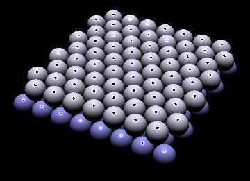

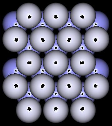


14 CVD growth of graphene and its functionalization A. Shikin, PRB (2000), Vol. 62 A. Varykhalov, PRL (2008), Vol Cracking of propylene on Ni(111) 2. Intercalation of Au into graphene/ni(111) Interface 3. Graphene layer bond to Ni is weakened A B
")
, Vol.")
15 Graphene/Ni(111) vs. Graphene/Au/Ni(111) A. Grüneis et al., PRB (2008), Vol. 77


 D.")
16 covalent functionalization: hydrogenated Graphene Energy [ev] K Momentum gap opening up when H applied! (consistent with theory) π band broadening ARPES provides a strategy to determine H-coverage: use ImΣ (lifetime) D. Haberer et al., Nano Lett. (2010), Vol. 10,


17 Energy Energy Momentum dispersion curves Momentum 0.8% 11% FWHM of MDCs continuously increasing k-k F
")
18 Energy Energy dispersion curves 0.8% Momentum pristine Graphene 0.5% H:C 5% H:C 17% H:C EDC maxima π band getting weaker depletion of PE Intensity at Fermi level (gap opening up) disorder induced MIT B. Dora et al. NJP 11, (2009)


19 ionic functionalization: n-doped Graphene rewind to Graphene/Au and insert additional electrons: Evaporation of potassium on Graphene/Au/Ni at ~30K warm up Intercalation of potassium between C/Au Interface


20 quasi-free-standing pristine and n-doped Graphene 0.5 Å -1 Graphene K Au Ni Å -1 π band shifted in energy after potassium doping, π* becomes visible

21 K-doping of Graphene/Au 0.1Å -1 K/C ~ 10% Intercalate K intercalated charge transfer to Graphene upon doping with K separation of π and π* after intercalation of K
 K intercalated: distance increased (~800meV) electron-phonon")
22 Energy Energy dispersion curves EDC K Momentum K on top: π band shifted in Energy, small separation of π, π* (~300meV) K intercalated: distance increased (~800meV) electron-phonon coupling visible*

23 covalent + ionic functionalization increasing distance between VB and CB due to chemisorption of hydrogen Fermi surface becomes smaller upon H new Level appears D. Haberer et al., submitted


24 Energy EDC cuts of hydrogenated n-doped Graphene EDC Momentum
25 Summary and Conclusions tunable bandgap acceptor level q-f-s Graphene: H-level above E F, not populated, not visible n-doped Graphene: H-level below E F + in the gap, visible

26 Apply CVD route to h-bn D. Usachov, D. Haberer et al., PRB (2010), Vol. 82 CVD on metal substrates not only suitable for Graphene h-bn can be synthesized, functionalized and even equipped with Graphene


27 Valence Band Properties of (C/)h-BN BN/Ni C/BN/Au BN/Au

28 Thank You for your Attention!

29 Summary and Conclusions tunable bandgap acceptor level q-f-s Graphene: H-level above E F, not populated, not visible n-doped Graphene: H-level below E F + in the gap, visible
Supplementary information for: Making graphene. nanoribbons photoluminescent
 Supplementary information for: Making graphene nanoribbons photoluminescent B.V. Senkovskiy,,,@ M. Pfeiffer,,@ S.K. Alavi,,,@ A. Bliesener, J. Zhu, S. Michel, A.V. Fedorov,,, R. German, D. Hertel, D. Haberer,
Minimal Update of Solid State Physics
 Minimal Update of Solid State Physics It is expected that participants are acquainted with basics of solid state physics. Therefore here we will refresh only those aspects, which are absolutely necessary
Overview. Carbon in all its forms. Background & Discovery Fabrication. Important properties. Summary & References. Overview of current research
 Graphene Prepared for Solid State Physics II Pr Dagotto Spring 2009 Laurene Tetard 03/23/09 Overview Carbon in all its forms Background & Discovery Fabrication Important properties Overview of current
ARPES experiments on 3D topological insulators. Inna Vishik Physics 250 (Special topics: spectroscopies of quantum materials) UC Davis, Fall 2016
 UC Davis, Fall 2016") ARPES experiments on 3D topological insulators Inna Vishik Physics 250 (Special topics: spectroscopies of quantum materials) UC Davis, Fall 2016 Outline Using ARPES to demonstrate that certain materials
ARPES experiments on 3D topological insulators Inna Vishik Physics 250 (Special topics: spectroscopies of quantum materials) UC Davis, Fall 2016 Outline Using ARPES to demonstrate that certain materials
Energy Spectroscopy. Ex.: Fe/MgO
 Energy Spectroscopy Spectroscopy gives access to the electronic properties (and thus chemistry, magnetism,..) of the investigated system with thickness dependence Ex.: Fe/MgO Fe O Mg Control of the oxidation
ESE 372 / Spring 2013 / Lecture 5 Metal Oxide Semiconductor Field Effect Transistor
 Metal Oxide Semiconductor Field Effect Transistor V G V G 1 Metal Oxide Semiconductor Field Effect Transistor We will need to understand how this current flows through Si What is electric current? 2 Back
Quantum Confinement in Graphene
 Quantum Confinement in Graphene from quasi-localization to chaotic billards MMM dominikus kölbl 13.10.08 1 / 27 Outline some facts about graphene quasibound states in graphene numerical calculation of
Transport through Andreev Bound States in a Superconductor-Quantum Dot-Graphene System
 Transport through Andreev Bound States in a Superconductor-Quantum Dot-Graphene System Nadya Mason Travis Dirk, Yung-Fu Chen, Cesar Chialvo Taylor Hughes, Siddhartha Lal, Bruno Uchoa Paul Goldbart University
Graphene. Tianyu Ye November 30th, 2011
 Graphene Tianyu Ye November 30th, 2011 Outline What is graphene? How to make graphene? (Exfoliation, Epitaxial, CVD) Is it graphene? (Identification methods) Transport properties; Other properties; Applications;
Band-like transport in highly crystalline graphene films from
 Supplementary figures Title: Band-like transport in highly crystalline graphene films from defective graphene oxides R. Negishi 1,*, M. Akabori 2, T. Ito 3, Y. Watanabe 4 and Y. Kobayashi 1 1 Department
& Dirac Fermion confinement Zahra Khatibi
 Graphene & Dirac Fermion confinement Zahra Khatibi 1 Outline: What is so special about Graphene? applications What is Graphene? Structure Transport properties Dirac fermions confinement Necessity External
Islamabad, Pakistan. Abstract
 Semiconductor-to-Metal Transition in the Bulk of WSe2 upon Potassium Intercalation Mushtaq Ahmad 1,2, Eric Müller 1, Carsten Habenicht 1, Roman Schuster 1, Martin Knupfer 1, and Bernd Büchner 1 1 IFW Dresden,
Graphene Novel Material for Nanoelectronics
 Graphene Novel Material for Nanoelectronics Shintaro Sato Naoki Harada Daiyu Kondo Mari Ohfuchi (Manuscript received May 12, 2009) Graphene is a flat monolayer of carbon atoms with a two-dimensional honeycomb
Nanostructured Carbon Allotropes as Weyl-Like Semimetals
 Nanostructured Carbon Allotropes as Weyl-Like Semimetals Shengbai Zhang Department of Physics, Applied Physics & Astronomy Rensselaer Polytechnic Institute symmetry In quantum mechanics, symmetry can be
Graphene films on silicon carbide (SiC) wafers supplied by Nitride Crystals, Inc.
 wafers supplied by Nitride Crystals, Inc.") 9702 Gayton Road, Suite 320, Richmond, VA 23238, USA Phone: +1 (804) 709-6696 info@nitride-crystals.com www.nitride-crystals.com Graphene films on silicon carbide (SiC) wafers supplied by Nitride Crystals,
9702 Gayton Road, Suite 320, Richmond, VA 23238, USA Phone: +1 (804) 709-6696 info@nitride-crystals.com www.nitride-crystals.com Graphene films on silicon carbide (SiC) wafers supplied by Nitride Crystals,
Supplementary Figure S1. AFM images of GraNRs grown with standard growth process. Each of these pictures show GraNRs prepared independently,
 Supplementary Figure S1. AFM images of GraNRs grown with standard growth process. Each of these pictures show GraNRs prepared independently, suggesting that the results is reproducible. Supplementary Figure
Hydrogenated Graphene
 Hydrogenated Graphene Stefan Heun NEST, Istituto Nanoscienze-CNR and Scuola Normale Superiore Pisa, Italy Outline Epitaxial Graphene Hydrogen Chemisorbed on Graphene Hydrogen-Intercalated Graphene Outline
Outline. Introduction: graphene. Adsorption on graphene: - Chemisorption - Physisorption. Summary
 Outline Introduction: graphene Adsorption on graphene: - Chemisorption - Physisorption Summary 1 Electronic band structure: Electronic properties K Γ M v F = 10 6 ms -1 = c/300 massless Dirac particles!
Basic cell design. Si cell
 Basic cell design Si cell 1 Concepts needed to describe photovoltaic device 1. energy bands in semiconductors: from bonds to bands 2. free carriers: holes and electrons, doping 3. electron and hole current:
EE143 Fall 2016 Microfabrication Technologies. Evolution of Devices
 EE143 Fall 2016 Microfabrication Technologies Prof. Ming C. Wu wu@eecs.berkeley.edu 511 Sutardja Dai Hall (SDH) 1-1 Evolution of Devices Yesterday s Transistor (1947) Today s Transistor (2006) 1-2 1 Why
Spin and angular resolved photoemission experiments on epitaxial graphene. Abstract
 Spin and angular resolved photoemission experiments on epitaxial graphene Isabella Gierz, 1, Jan Hugo Dil, 2, 3 Fabian Meier, 2, 3 Bartosz Slomski, 2, 3 Jürg Osterwalder, 3 Jürgen Henk, 4 Roland Winkler,
Impurities and graphene hybrid structures: insights from first-principles theory
 Impurities and graphene hybrid structures: insights from first-principles theory Tim Wehling Institute for Theoretical Physics and Bremen Center for Computational Materials Science University of Bremen
Studying Metal to Insulator Transitions in Solids using Synchrotron Radiation-based Spectroscopies.
 PY482 Lecture. February 28 th, 2013 Studying Metal to Insulator Transitions in Solids using Synchrotron Radiation-based Spectroscopies. Kevin E. Smith Department of Physics Department of Chemistry Division
Optimizing Graphene Morphology on SiC(0001)
") Optimizing Graphene Morphology on SiC(0001) James B. Hannon Rudolf M. Tromp Graphene sheets Graphene sheets can be formed into 0D,1D, 2D, and 3D structures Chemically inert Intrinsically high carrier mobility
Optimizing Graphene Morphology on SiC(0001) James B. Hannon Rudolf M. Tromp Graphene sheets Graphene sheets can be formed into 0D,1D, 2D, and 3D structures Chemically inert Intrinsically high carrier mobility
Ch. 2: Energy Bands And Charge Carriers In Semiconductors
 Ch. 2: Energy Bands And Charge Carriers In Semiconductors Discrete energy levels arise from balance of attraction force between electrons and nucleus and repulsion force between electrons each electron
SiC Graphene Suitable For Quantum Hall Resistance Metrology.
 SiC Graphene Suitable For Quantum Hall Resistance Metrology. Samuel Lara-Avila 1, Alexei Kalaboukhov 1, Sara Paolillo, Mikael Syväjärvi 3, Rositza Yakimova 3, Vladimir Fal'ko 4, Alexander Tzalenchuk 5,
Comment on A de Haas-van Alphen study of the Fermi surfaces of superconducting LiFeP and LiFeAs
 Comment on A de Haas-van Alphen study of the Fermi surfaces of superconducting LiFeP and LiFeAs S.V. Borisenko, 1 V. B. Zabolotnyy, 1 D.V. Evtushinsky, 1 T. K. Kim, 1,2 I.V. Morozov, 1,3 A. A. Kordyuk,
Topological Insulators and Ferromagnets: appearance of flat surface bands
 Topological Insulators and Ferromagnets: appearance of flat surface bands Thomas Dahm University of Bielefeld T. Paananen and T. Dahm, PRB 87, 195447 (2013) T. Paananen et al, New J. Phys. 16, 033019 (2014)
Graphene and Quantum Hall (2+1)D Physics
D Physics") The 4 th QMMRC-IPCMS Winter School 8 Feb 2011, ECC, Seoul, Korea Outline 2 Graphene and Quantum Hall (2+1)D Physics Lecture 1. Electronic structures of graphene and bilayer graphene Lecture 2. Electrons
The 4 th QMMRC-IPCMS Winter School 8 Feb 2011, ECC, Seoul, Korea Outline 2 Graphene and Quantum Hall (2+1)D Physics Lecture 1. Electronic structures of graphene and bilayer graphene Lecture 2. Electrons
ELEMENTARY BAND THEORY
 ELEMENTARY BAND THEORY PHYSICIST Solid state band Valence band, VB Conduction band, CB Fermi energy, E F Bloch orbital, delocalized n-doping p-doping Band gap, E g Direct band gap Indirect band gap Phonon
Direct and Indirect Semiconductor
 Direct and Indirect Semiconductor Allowed values of energy can be plotted vs. the propagation constant, k. Since the periodicity of most lattices is different in various direction, the E-k diagram must
So why is sodium a metal? Tungsten Half-filled 5d band & half-filled 6s band. Insulators. Interaction of metals with light?
 Bonding in Solids: Metals, Insulators, & CHEM 107 T. Hughbanks Delocalized bonding in Solids Think of a pure solid as a single, very large molecule. Use our bonding pictures to try to understand properties.
CVD growth of Graphene. SPE ACCE presentation Carter Kittrell James M. Tour group September 9 to 11, 2014
 CVD growth of Graphene SPE ACCE presentation Carter Kittrell James M. Tour group September 9 to 11, 2014 Graphene zigzag armchair History 1500: Pencil-Is it made of lead? 1789: Graphite 1987: The first
Spring 2010 MSE 111. Midterm Exam. Prof. Eugene E. Haller. University of California at Berkeley Department of Materials Science and Engineering
 Spring 00 MS Midterm xam Prof. ugene. Haller University of California at Berkeley Department of Materials Science and ngineering 3/6/0, 9:40 am 80 minutes, 74 points total, 0 pages ame: SID: Problem 3
Strong Correlation Effects in Fullerene Molecules and Solids
 Strong Correlation Effects in Fullerene Molecules and Solids Fei Lin Physics Department, Virginia Tech, Blacksburg, VA 2461 Fei Lin (Virginia Tech) Correlations in Fullerene SESAPS 211, Roanoke, VA 1 /
(a) (b) Supplementary Figure 1. (a) (b) (a) Supplementary Figure 2. (a) (b) (c) (d) (e)
 (b) Supplementary Figure 1. (a) (b) (a) Supplementary Figure 2. (a) (b) (c) (d) (e)") (a) (b) Supplementary Figure 1. (a) An AFM image of the device after the formation of the contact electrodes and the top gate dielectric Al 2 O 3. (b) A line scan performed along the white dashed line
(a) (b) Supplementary Figure 1. (a) An AFM image of the device after the formation of the contact electrodes and the top gate dielectric Al 2 O 3. (b) A line scan performed along the white dashed line
Physics and Material Science of Semiconductor Nanostructures
 Physics and Material Science of Semiconductor Nanostructures PHYS 570P Prof. Oana Malis Email: omalis@purdue.edu Course website: http://www.physics.purdue.edu/academic_programs/courses/phys570p/ 1 Introduction
JOURNAL OF MATHEMATICAL NANOSCIENCE. Band gap modulation of graphyne: A density functional theory study ROYA MAJIDI
 JOURNAL OF MATHEMATICAL NANOSCIENCE Vol. 4, No. 1-2, 2015, 11-22 Band gap modulation of graphyne: A density functional theory study ROYA MAJIDI Department of Physics, Faculty of Science, Shahid Rajaee
Supplementary Materials for
 advances.sciencemag.org/cgi/content/full/4/9/eaat8355/dc1 Supplementary Materials for Electronic structures and unusually robust bandgap in an ultrahigh-mobility layered oxide semiconductor, Bi 2 O 2 Se
Semiconductor Physics and Devices Chapter 3.
 Introduction to the Quantum Theory of Solids We applied quantum mechanics and Schrödinger s equation to determine the behavior of electrons in a potential. Important findings Semiconductor Physics and
Graphene and Carbon Nanotubes
 Graphene and Carbon Nanotubes 1 atom thick films of graphite atomic chicken wire Novoselov et al - Science 306, 666 (004) 100μm Geim s group at Manchester Novoselov et al - Nature 438, 197 (005) Kim-Stormer
Visualizing Electronic Structures of Quantum Materials By Angle Resolved Photoemission Spectroscopy (ARPES)
") Visualizing Electronic Structures of Quantum Materials By Angle Resolved Photoemission Spectroscopy (ARPES) PART A: ARPES & Application Yulin Chen Oxford University / Tsinghua University www.arpes.org.uk
Visualizing Electronic Structures of Quantum Materials By Angle Resolved Photoemission Spectroscopy (ARPES) PART A: ARPES & Application Yulin Chen Oxford University / Tsinghua University www.arpes.org.uk
Introduction of XPS Absolute binding energies of core states Applications to silicone Outlook
 Core level binding energies in solids from first-principles Introduction of XPS Absolute binding energies of core states Applications to silicone Outlook TO and C.-C. Lee, Phys. Rev. Lett. 118, 026401
per unit cell Motif: Re at (0, 0, 0); 3O at ( 1 / 2, 0), (0, 0, 1 / 2 ) Re: 6 (octahedral coordination) O: 2 (linear coordination) ReO 6
; 3O at ( 1 / 2, 0), (0, 0, 1 / 2 ) Re: 6 (octahedral coordination) O: 2 (linear coordination) ReO 6") Lattice: Primitive Cubic 1ReO 3 per unit cell Motif: Re at (0, 0, 0); 3O at ( 1 / 2, 0, 0), (0, 1 / 2, 0), (0, 0, 1 / 2 ) Re: 6 (octahedral coordination) O: 2 (linear coordination) ReO 6 octahedra share
Lattice: Primitive Cubic 1ReO 3 per unit cell Motif: Re at (0, 0, 0); 3O at ( 1 / 2, 0, 0), (0, 1 / 2, 0), (0, 0, 1 / 2 ) Re: 6 (octahedral coordination) O: 2 (linear coordination) ReO 6 octahedra share
2D Materials with Strong Spin-orbit Coupling: Topological and Electronic Transport Properties
 2D Materials with Strong Spin-orbit Coupling: Topological and Electronic Transport Properties Artem Pulkin California Institute of Technology (Caltech), Pasadena, CA 91125, US Institute of Physics, Ecole
Physical Properties of Mono-layer of
 Chapter 3 Physical Properties of Mono-layer of Silicene The fascinating physical properties[ 6] associated with graphene have motivated many researchers to search for new graphene-like two-dimensional
single-layer transition metal dichalcogenides MC2
 single-layer transition metal dichalcogenides MC2 Period 1 1 H 18 He 2 Group 1 2 Li Be Group 13 14 15 16 17 18 B C N O F Ne 3 4 Na K Mg Ca Group 3 4 5 6 7 8 9 10 11 12 Sc Ti V Cr Mn Fe Co Ni Cu Zn Al Ga
The many forms of carbon
 The many forms of carbon Carbon is not only the basis of life, it also provides an enormous variety of structures for nanotechnology. This versatility is connected to the ability of carbon to form two
Review of Semiconductor Fundamentals
 ECE 541/ME 541 Microelectronic Fabrication Techniques Review of Semiconductor Fundamentals Zheng Yang (ERF 3017, email: yangzhen@uic.edu) Page 1 Semiconductor A semiconductor is an almost insulating material,
arxiv: v1 [cond-mat.mtrl-sci] 9 Mar 2013
![arxiv: v1 [cond-mat.mtrl-sci] 9 Mar 2013](/thumbs/86/94109325.jpg "arxiv: v1 [cond-mat.mtrl-sci] 9 Mar 2013") Stacked topological insulator built from bismuth-based graphene sheet analogues Bertold Rasche 1, Anna Isaeva 1, Michael Ruck 1,2, Sergey Borisenko 3, Volodymyr Zabolotnyy 3, Bernd Büchner 3,4, Klaus Koepernik
Stacked topological insulator built from bismuth-based graphene sheet analogues Bertold Rasche 1, Anna Isaeva 1, Michael Ruck 1,2, Sergey Borisenko 3, Volodymyr Zabolotnyy 3, Bernd Büchner 3,4, Klaus Koepernik
Quiz #1 Practice Problem Set
 Name: Student Number: ELEC 3908 Physical Electronics Quiz #1 Practice Problem Set? Minutes January 22, 2016 - No aids except a non-programmable calculator - All questions must be answered - All questions
Lecture 1. OUTLINE Basic Semiconductor Physics. Reading: Chapter 2.1. Semiconductors Intrinsic (undoped) silicon Doping Carrier concentrations
 silicon Doping Carrier concentrations") Lecture 1 OUTLINE Basic Semiconductor Physics Semiconductors Intrinsic (undoped) silicon Doping Carrier concentrations Reading: Chapter 2.1 EE105 Fall 2007 Lecture 1, Slide 1 What is a Semiconductor? Low
Lecture 1 OUTLINE Basic Semiconductor Physics Semiconductors Intrinsic (undoped) silicon Doping Carrier concentrations Reading: Chapter 2.1 EE105 Fall 2007 Lecture 1, Slide 1 What is a Semiconductor? Low
Initial Stages of Growth of Organic Semiconductors on Graphene
 Initial Stages of Growth of Organic Semiconductors on Graphene Presented by: Manisha Chhikara Supervisor: Prof. Dr. Gvido Bratina University of Nova Gorica Outline Introduction to Graphene Fabrication
Semiconductor-Detectors
 Semiconductor-Detectors 1 Motivation ~ 195: Discovery that pn-- junctions can be used to detect particles. Semiconductor detectors used for energy measurements ( Germanium) Since ~ 3 years: Semiconductor
Advantages / Disadvantages of semiconductor detectors
 Advantages / Disadvantages of semiconductor detectors Semiconductor detectors have a high density (compared to gas detector) large energy loss in a short distance diffusion effect is smaller than in gas
Hole-concentration dependence of band structure in (Bi,Pb) 2 (Sr,La) 2 CuO 6+δ determined by the angle-resolved photoemission spectroscopy
 2 (Sr,La) 2 CuO 6+δ determined by the angle-resolved photoemission spectroscopy") Journal of Electron Spectroscopy and Related Phenomena 137 140 (2004) 663 668 Hole-concentration dependence of band structure in (Bi,Pb) 2 (Sr,La) 2 CuO 6+δ determined by the angle-resolved photoemission
Journal of Electron Spectroscopy and Related Phenomena 137 140 (2004) 663 668 Hole-concentration dependence of band structure in (Bi,Pb) 2 (Sr,La) 2 CuO 6+δ determined by the angle-resolved photoemission
Ph D in Physics from the University of Toulouse (UPS) and Post Graduate Diploma in research (HDR) from University of Grenoble (France).
 and Post Graduate Diploma in research (HDR) from University of Grenoble (France).") Aziz ZENASNI Ph D in Physics from the University of Toulouse (UPS) and Post Graduate Diploma in research (HDR) from University of Grenoble (France). Currently a Research Staff Member of CEA-LETI, he has
Aziz ZENASNI Ph D in Physics from the University of Toulouse (UPS) and Post Graduate Diploma in research (HDR) from University of Grenoble (France). Currently a Research Staff Member of CEA-LETI, he has
Supporting Information
 Supporting Information Conversion of multilayer graphene into continuous ultrathin sp 3 - bonded carbon films on metal surfaces Dorj Odkhuu 1, Dongbin Shin 2, Rodney S. Ruoff 3, and Noejung Park 1,2 1
XPS Depth Profiling of Epitaxial Graphene Intercalated with FeCl 3
 XPS Depth Profiling of Epitaxial Graphene Intercalated with FeCl 3 Mahdi Ibrahim Maynard H. Jackson High School Atlanta, GA. Faculty Advisor: Dr. Kristin Shepperd Research Group: Prof. Edward Conrad School
arxiv: v1 [cond-mat.mtrl-sci] 3 May 2015
![arxiv: v1 [cond-mat.mtrl-sci] 3 May 2015](/thumbs/94/118238290.jpg "arxiv: v1 [cond-mat.mtrl-sci] 3 May 2015") Semiconducting graphene from highly ordered substrate interactions M.S. Nevius,1 M. Conrad,1 F. Wang,1 A. Celis,2, 3 M.N. Nair,4 A. Taleb-Ibrahimi,4 A. Tejeda,2, 3 and E.H. Conrad1, 1 arxiv:1505.00435v1
Semiconducting graphene from highly ordered substrate interactions M.S. Nevius,1 M. Conrad,1 F. Wang,1 A. Celis,2, 3 M.N. Nair,4 A. Taleb-Ibrahimi,4 A. Tejeda,2, 3 and E.H. Conrad1, 1 arxiv:1505.00435v1
3D Weyl metallic states realized in the Bi 1-x Sb x alloy and BiTeI. Heon-Jung Kim Department of Physics, Daegu University, Korea
 3D Weyl metallic states realized in the Bi 1-x Sb x alloy and BiTeI Heon-Jung Kim Department of Physics, Daegu University, Korea Content 3D Dirac metals Search for 3D generalization of graphene Bi 1-x
Surface Transfer Doping of Diamond by Organic Molecules
 Surface Transfer Doping of Diamond by Organic Molecules Qi Dongchen Department of Physics National University of Singapore Supervisor: Prof. Andrew T. S. Wee Dr. Gao Xingyu Scope of presentation Overview
arxiv: v1 [cond-mat.supr-con] 20 Mar 2013
![arxiv: v1 [cond-mat.supr-con] 20 Mar 2013](/thumbs/81/83806986.jpg "arxiv: v1 [cond-mat.supr-con] 20 Mar 2013") Challenging the nature of low energy plasmon excitations in CaC6 using electron energy-loss spectroscopy Friedrich Roth,1 Andreas Ko nig,1 Christian Kramberger,2 Thomas Pichler,2 Bernd Bu chner,1 and Martin
Challenging the nature of low energy plasmon excitations in CaC6 using electron energy-loss spectroscopy Friedrich Roth,1 Andreas Ko nig,1 Christian Kramberger,2 Thomas Pichler,2 Bernd Bu chner,1 and Martin
E lectrons in condensed matter generally behave as semi-classical particles. In certain materials systems,
 OPEN SUBJECT AREAS: TOPOLOGICAL INSULATORS ELECTRONIC PROPERTIES AND MATERIALS Received 16 April 2014 Accepted 14 May 2014 Published 4 June 2014 Correspondence and requests for materials should be addressed
Supporting Information
 Electronic Supplementary Material (ESI) for Nanoscale. This journal is The Royal Society of Chemistry 2015 Supporting Information Single Layer Lead Iodide: Computational Exploration of Structural, Electronic
On surface synthesis of a 2D boroxine framework: a route to a novel 2D material?
 Electronic Supplementary Material (ESI) for ChemComm. This journal is The Royal Society of Chemistry 2018 On surface synthesis of a 2D boroxine framework: a route to a novel 2D material? Matus Stredansky,
3. Two-dimensional systems
 3. Two-dimensional systems Image from IBM-Almaden 1 Introduction Type I: natural layered structures, e.g., graphite (with C nanostructures) Type II: artificial structures, heterojunctions Great technological
Photoemission Studies of Strongly Correlated Systems
 Photoemission Studies of Strongly Correlated Systems Peter D. Johnson Physics Dept., Brookhaven National Laboratory JLab March 2005 MgB2 High T c Superconductor - Phase Diagram Fermi Liquid:-Excitations
Quantum anomalous Hall states on decorated magnetic surfaces
 Quantum anomalous Hall states on decorated magnetic surfaces David Vanderbilt Rutgers University Kevin Garrity & D.V. Phys. Rev. Lett.110, 116802 (2013) Recently: Topological insulators (TR-invariant)
On the Possible new High Temperature Superconductors. Zhi Cheng (9 Bairong st. Baiyun District, Guangzhou, China
 On the Possible new High Temperature Superconductors Zhi Cheng (9 Bairong st. Baiyun District, Guangzhou, China. 510400. gzchengzhi@hotmail.com) Abstract: It shows that the hybrid graphene may be the high
NanoEngineering of Hybrid Carbon Nanotube Metal Composite Materials for Hydrogen Storage Anders Nilsson
 NanoEngineering of Hybrid Carbon Nanotube Metal Composite Materials for Hydrogen Storage Anders Nilsson Stanford Synchrotron Radiation Laboratory (SSRL) and Stockholm University Coworkers and Ackowledgement
Angle-resolved photoemission study of the graphite intercalation compound KC 8 : A key to graphene
 Angle-resolved photoemission study of the graphite intercalation compound KC 8 : A key to graphene A. Grüneis, 1,2, * C. Attaccalite, 3 A. Rubio, 3,4 D. V. Vyalikh, 5 S. L. Molodtsov, 5 J. Fink, 2,6 R.
Supplementary Figures
 Supplementary Figures Supplementary Figure 1: Region mapping. a Pristine and b Mn-doped Bi 2 Te 3. Arrows point at characteristic defects present on the pristine surface which have been used as markers
Semiconductors and Optoelectronics. Today Semiconductors Acoustics. Tomorrow Come to CH325 Exercises Tours
 Semiconductors and Optoelectronics Advanced Physics Lab, PHYS 3600 Don Heiman, Northeastern University, 2017 Today Semiconductors Acoustics Tomorrow Come to CH325 Exercises Tours Semiconductors and Optoelectronics
Surface Science Reports. The surface science of graphene: Metal interfaces, CVD synthesis, nanoribbons, chemical modifications, and defects
 Surface Science Reports 67 (2012) 83 115 Contents lists available at SciVerse ScienceDirect Surface Science Reports journal homepage: www.elsevier.com/locate/surfrep The surface science of graphene: Metal
arxiv: v1 [cond-mat.mtrl-sci] 11 May 2014
![arxiv: v1 [cond-mat.mtrl-sci] 11 May 2014](/thumbs/94/119491084.jpg "arxiv: v1 [cond-mat.mtrl-sci] 11 May 2014") General approach to the understanding the electronic structure of graphene on metals E. N. Voloshina a Institut für Chemie, Humboldt-Universität zu Berlin, 10099 Berlin, Germany arxiv:1405.2556v1 [cond-mat.mtrl-sci]
General approach to the understanding the electronic structure of graphene on metals E. N. Voloshina a Institut für Chemie, Humboldt-Universität zu Berlin, 10099 Berlin, Germany arxiv:1405.2556v1 [cond-mat.mtrl-sci]
SIGNATURES OF SPIN-ORBIT DRIVEN ELECTRONIC TRANSPORT IN TRANSITION- METAL-OXIDE INTERFACES
 SIGNATURES OF SPIN-ORBIT DRIVEN ELECTRONIC TRANSPORT IN TRANSITION- METAL-OXIDE INTERFACES Nicandro Bovenzi Bad Honnef, 19-22 September 2016 LAO/STO heterostructure: conducting interface between two insulators
Spectro-microscopy of single and multi-layer graphene supported by a weakly. interacting substrate
 Spectro-microscopy of single and multi-layer graphene supported by a weakly interacting substrate Kevin R. Knox 1,2, Shancai Wang 2, Alberto Morgante 3,4 Dean Cvetko 3,5, Andrea Locatelli 6, Tevfik Onur
arxiv:cond-mat/ v1 [cond-mat.supr-con] 28 May 2003
![arxiv:cond-mat/ v1 [cond-mat.supr-con] 28 May 2003](/thumbs/96/128981112.jpg "arxiv:cond-mat/ v1 [cond-mat.supr-con] 28 May 2003") arxiv:cond-mat/0305637v1 [cond-mat.supr-con] 28 May 2003 The superconducting state in a single CuO 2 layer: Experimental findings and scenario Rushan Han, Wei Guo School of Physics, Peking University,
arxiv:cond-mat/0305637v1 [cond-mat.supr-con] 28 May 2003 The superconducting state in a single CuO 2 layer: Experimental findings and scenario Rushan Han, Wei Guo School of Physics, Peking University,
Electron-phonon calculations for metals, insulators, and superconductors
 Electron-phonon calculations for metals, insulators, and superconductors Feliciano Giustino Department of Materials, University of Oxford TALK OUTLINE Metals Insulators Superconductors THE WONDER ELEMENT
Out-of-equilibrium electron dynamics in photoexcited topological insulators studied by TR-ARPES
 Cliquez et modifiez le titre Out-of-equilibrium electron dynamics in photoexcited topological insulators studied by TR-ARPES Laboratoire de Physique des Solides Orsay, France June 15, 2016 Workshop Condensed
SCIENCE & TECHNOLOGY
 Pertanika J. Sci. & Technol. 25 (S): 205-212 (2017) SCIENCE & TECHNOLOGY Journal homepage: http://www.pertanika.upm.edu.my/ Effect of Boron and Oxygen Doping to Graphene Band Structure Siti Fazlina bt
Lectures Graphene and
 Lectures 15-16 Graphene and carbon nanotubes Graphene is atomically thin crystal of carbon which is stronger than steel but flexible, is transparent for light, and conducts electricity (gapless semiconductor).
EECS143 Microfabrication Technology
 EECS143 Microfabrication Technology Professor Ali Javey Introduction to Materials Lecture 1 Evolution of Devices Yesterday s Transistor (1947) Today s Transistor (2006) Why Semiconductors? Conductors e.g
Ferromagnetism and Anomalous Hall Effect in Graphene
 Ferromagnetism and Anomalous Hall Effect in Graphene Jing Shi Department of Physics & Astronomy, University of California, Riverside Graphene/YIG Introduction Outline Proximity induced ferromagnetism Quantized
Supplementary information for. Evolution of the Valley Position in Bulk Transition-Metal Chalcogenides and. their Mono-Layer Limit
 Supplementary information for Evolution of the Valley Position in Bulk Transition-Metal Chalcogenides and their Mono-Layer Limit Hongtao Yuan 1,2, Zhongkai Liu 1,2,3,4, Gang Xu 1, Bo Zhou 5,6, Sanfeng
Electronic properties of graphene. Jean-Noël Fuchs Laboratoire de Physique des Solides Université Paris-Sud (Orsay)
") Electronic properties of graphene Jean-Noël Fuchs Laboratoire de Physique des Solides Université Paris-Sud (Orsay) Cargèse, September 2012 3 one-hour lectures in 2 x 1,5h on electronic properties of graphene
Electronic properties of graphene Jean-Noël Fuchs Laboratoire de Physique des Solides Université Paris-Sud (Orsay) Cargèse, September 2012 3 one-hour lectures in 2 x 1,5h on electronic properties of graphene
ECE 442. Spring, Lecture -2
 ECE 442 Power Semiconductor Devices and Integrated circuits Spring, 2006 University of Illinois at Chicago Lecture -2 Semiconductor physics band structures and charge carriers 1. What are the types of
SEMICONDUCTOR PHYSICS
 SEMICONDUCTOR PHYSICS by Dibyendu Chowdhury Semiconductors The materials whose electrical conductivity lies between those of conductors and insulators, are known as semiconductors. Silicon Germanium Cadmium
Tight-binding description of the quasiparticle dispersion of graphite and few-layer graphene
 Tight-binding description of the quasiparticle dispersion of graphite and few-layer graphene A. Grüneis, 1,2, * C. Attaccalite, 3,4 L. Wirtz, 4 H. Shiozawa, 5 R. Saito, 6 T. Pichler, 1 and A. Rubio 3 1
Theory of doping graphene
 H. Pinto, R. Jones School of Physics, University of Exeter, EX4 4QL, Exeter United Kingdom May 25, 2010 Graphene Graphene is made by a single atomic layer of carbon atoms arranged in a honeycomb lattice.
Charge Carriers in Semiconductor
 Charge Carriers in Semiconductor To understand PN junction s IV characteristics, it is important to understand charge carriers behavior in solids, how to modify carrier densities, and different mechanisms
arxiv: v1 [cond-mat.mtrl-sci] 12 Oct 2007
![arxiv: v1 [cond-mat.mtrl-sci] 12 Oct 2007](/thumbs/72/67208262.jpg "arxiv: v1 [cond-mat.mtrl-sci] 12 Oct 2007") A possible source of spin-polarized electrons: The inert graphene/ni(111) system arxiv:0710.2514v1 [cond-mat.mtrl-sci] 12 Oct 2007 Yu. S. Dedkov and C. Laubschat Institut für Festkörperphysik, Technische
A possible source of spin-polarized electrons: The inert graphene/ni(111) system arxiv:0710.2514v1 [cond-mat.mtrl-sci] 12 Oct 2007 Yu. S. Dedkov and C. Laubschat Institut für Festkörperphysik, Technische
GRAPHENE the first 2D crystal lattice
 GRAPHENE the first 2D crystal lattice dimensionality of carbon diamond, graphite GRAPHENE realized in 2004 (Novoselov, Science 306, 2004) carbon nanotubes fullerenes, buckyballs what s so special about
Electron Energy, E E = 0. Free electron. 3s Band 2p Band Overlapping energy bands. 3p 3s 2p 2s. 2s Band. Electrons. 1s ATOM SOLID.
 Electron Energy, E Free electron Vacuum level 3p 3s 2p 2s 2s Band 3s Band 2p Band Overlapping energy bands Electrons E = 0 1s ATOM 1s SOLID In a metal the various energy bands overlap to give a single
SUPPLEMENTARY INFORMATION
 DOI: 1.138/NMAT3449 Topological crystalline insulator states in Pb 1 x Sn x Se Content S1 Crystal growth, structural and chemical characterization. S2 Angle-resolved photoemission measurements at various
Carbon based Nanoscale Electronics
 Carbon based Nanoscale Electronics 09 02 200802 2008 ME class Outline driving force for the carbon nanomaterial electronic properties of fullerene exploration of electronic carbon nanotube gold rush of
Supplementary Figure 1 Magneto-transmission spectra of graphene/h-bn sample 2 and Landau level transition energies of three other samples.
 Supplementary Figure 1 Magneto-transmission spectra of graphene/h-bn sample 2 and Landau level transition energies of three other samples. (a,b) Magneto-transmission ratio spectra T(B)/T(B 0 ) of graphene/h-bn
Resonant Inelastic X-ray Scattering on elementary excitations
 Resonant Inelastic X-ray Scattering on elementary excitations Jeroen van den Brink Ament, van Veenendaal, Devereaux, Hill & JvdB Rev. Mod. Phys. 83, 705 (2011) Autumn School in Correlated Electrons Jülich
Tailoring the electronic properties of low-dimensional carbon hybrids
 Tailoring the electronic properties of low-dimensional carbon hybrids Thomas Pichler University of Vienna Faculty of Physics Tokyo 5.10.2012 Acknowledgements Vienna University group: C. Kramberger, A.