SEMICONDUCTOR PHYSICS
|
|
|
- Kory Gordon
- 5 years ago
- Views:
Transcription
1 SEMICONDUCTOR PHYSICS by Dibyendu Chowdhury
2 Semiconductors The materials whose electrical conductivity lies between those of conductors and insulators, are known as semiconductors. Silicon Germanium Cadmium Sulphide 1.1 ev 0.7 ev 2.4 ev Silicon is the most widely used semiconductor. Semiconductors have negative temperature coefficients of resistance, i.e. as temperature increases resistivity deceases

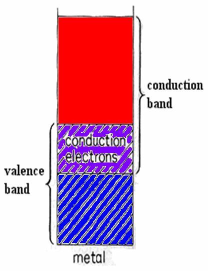
3 Energy Band Diagram Conduction electrons

4 Energy Band Diagram Forbidden energy band is small for semiconductors. Less energy is required for electron to move from valence to conduction band. A vacancy (hole) remains when an electron leaves the valence band. Hole acts as a positive charge carrier.
5 Both silicon and germanium are tetravalent, i.e. each has four electrons (valence electrons) in their outermost shell. Intrinsic Semiconductor A semiconductor, which is in its extremely pure form, is known as an intrinsic semiconductor. Silicon and germanium are the most widely used intrinsic semiconductors. Each atom shares its four valence electrons with its four immediate neighbours, so that each atom is involved in four covalent bonds.
6 Intrinsic Semiconductor When the temperature of an intrinsic semiconductor is increased, beyond room temperature a large number of electron-hole pairs are generated. Since the electron and holes are generated in pairs so, Free electron concentration (n) = concentration of holes (p) = Intrinsic carrier concentration (n i )
7 Extrinsic Semiconductor Pure semiconductors have negligible conductivity at room temperature. To increase the conductivity of intrinsic semiconductor, some impurity is added. The resulting semiconductor is called impure or extrinsic semiconductor. Impurities are added at the rate of ~ one atom per 10 6 to semiconductor atoms. The purpose of adding impurity is to increase either the number of free electrons or holes in a semiconductor.
8 Extrinsic Semiconductor Two types of impurity atoms are added to the semiconductor Atoms containing 5 valance electrons (Pentavalent impurity atoms) e.g. P, As, Sb, Bi Atoms containing 3 valance electrons (Trivalent impurity atoms) e.g. Al, Ga, B, In N-type semiconductor P-type semiconductor
9 N-type Semiconductor The semiconductors which are obtained by introducing pentavalent impurity atoms are known as N-type semiconductors. Examples are P, Sb, As and Bi. These elements have 5 electrons in their valance shell. Out of which 4 electrons will form covalent bonds with the neighbouring atoms and the 5 th electron will be available as a current carrier. The impurity atom is thus known as donor atom. In N-type semiconductor current flows due to the movement of electrons and holes but majority of through electrons. Thus electrons in a N-type semiconductor are known as majority charge carriers while holes as minority charge carriers.
10 P-type Semiconductor The semiconductors which are obtained by introducing trivalent impurity atoms are known as P-type semiconductors. Examples are Ga, In, Al and B. These elements have 3 electrons in their valance shell which will form covalent bonds with the neighbouring atoms. The fourth covalent bond will remain incomplete. A vacancy, which exists in the incomplete covalent bond constitute a hole. The impurity atom is thus known as acceptor atom. In P-type semiconductor current flows due to the movement of electrons and holes but majority of through holes. Thus holes in a P- type semiconductor are known as majority charge carriers while electrons as minority charge carriers.
11 Fermi Energy The Fermi energy is a quantum mechanical concept and it usually refers to the energy of the highest occupied quantum state in a system of fermions at absolute zero temperature.. Fermi Level The Fermi level (E F ) is the maximum energy, which can be occupied by an electron at absolute zero (0 K).
 The Fermi level (E F ) lies at the middle of the forbidden energy")
12 Fermi Energy Diagram for Intrinsic Semiconductors Forbidden Energy Gap Fermi Level (E F ) The Fermi level (E F ) lies at the middle of the forbidden energy gap.
13 Fermi Energy Diagram for N-type Semiconductors Fermi Level (E F ) Energy (ev) Donor Level Fermi Level (E F ) The Fermi level (E F ) shifts upwards towards the bottom of the conduction band.
14 Fermi Energy Diagram for P-type Semiconductors Energy (ev) Acceptor Level Fermi Level (E F ) Fermi Level (E F ) The Fermi level (E F ) shifts downwards towards the top of the valance band.
15 Mass Action Law Addition of n-type impurities decreases the number of holes below a level. Similarly, the addition of p-type impurities decreases the number of electrons below a level. It has been experimentally found that Under thermal equilibrium for any semiconductor, the product of no. of holes and the no. of electrons is constant and independent of amount of doping. This relation is known as mass action law n 2. p ni where n = electron concentration, p = hole concentration and n i = intrinsic concentration
16 Charge carrier concentration in N-type and P-type Semiconductors The free electron and hole concentrations are related by the Law of Electrical Neutrality i.e. Total positive charge density is equal to the total negative charge density Let N D = Concentration of donor atoms = no. of positive charges/m 3 contributed by donor ions p = hole concentration N A =Concentration of acceptor atoms n = electron concentration By the law of electrical neutrality N D + p = N A + n
17 For N-Type semiconductor N A = 0 i.e. Concentration of acceptor atoms And n>>p, then N D + 0 = 0 + n N D = n i.e. in N-type, concentration of donor atoms is equal to the concentration of free electrons. According to Mass Action Law n 2. p ni p n / n n / 2 i 2 i N D
18 For P-Type semiconductor N D = 0 i.e. Concentration of donor atoms And p>>n, then N A + 0 = 0 + p N A = p i.e. in P-type, concentration of acceptor atoms is equal to the concentration of holes. According to Mass Action Law n 2. p ni n n / p n / 2 i 2 i N A
19 The Concept of Effective Mass : Comparing Free e - in vacuum In an electric field m o =9.1 x Free electron mass An e - in a crystal In an electric field In a crystal If the same magnitude of electric field is applied to both electrons in vacuum and inside the crystal, the electrons will accelerate at a different rate from each other due to the existence of different potentials inside the crystal. The electron inside the crystal has to try to make its own way. So the electrons inside the crystal will have a different mass than that of the electron in vacuum. m =? m * effective mass This altered mass is called as an effective-mass.

20 What is the expression for m * Particles of electrons and holes behave as a wave under certain conditions. So one has to consider the de Broglie wavelength to link partical behaviour with wave behaviour. Partical such as electrons and waves can be diffracted from the crystal just as X-rays. Certain electron momentum is not allowed by the crystal lattice. This is the origin of the energy band gaps. n 2d sin n = the order of the diffraction λ = the wavelength of the X-ray d = the distance between planes θ = the incident angle of the X-ray beam
21 n = 2d The waves are standing waves = 2 k The momentum is P = k (1) is the propogation constant The energy of the free electron can be related to its momentum E E (2) 2 h P P = = 2m free e - mass, m h h 2m 2m = h 2 E k2 2m k (2 ) The energy of the free e - is related to the k By means of equations (1) and (2) certain e - momenta are not allowed by the crystal. The velocity of the electron at these momentum values is zero. Energy momentum E versus k diagram is a parabola. Energy is continuous with k, i,e, all energy (momentum) values are allowed. E versus k diagram or Energy versus momentum diagrams k
22 To find effective mass, m * We will take the derivative of energy with respect to k ; de dk d E 2 dk 2 k m m m* is determined by the curvature of the E-k curve - m* is inversely proportional to the curvature Change m* instead of m m * d E dk This formula is the effective mass of an electron inside the crystal.
23 Direct an indirect-band gap materials : Direct-band gap s/c s (e.g. GaAs, InP, AlGaAs) CB E For a direct-band gap material, the minimum of the conduction band and maximum of the valance band lies at the same momentum, k, values. e - + k When an electron sitting at the bottom of the CB recombines with a hole sitting at the top of the VB, there will be no change in momentum values. VB Energy is conserved by means of emitting a photon, such transitions are called as radiative transitions.
24 Indirect-band gap s/c s (e.g. Si and Ge) E For an indirect-band gap material; the minimum of the CB and maximum of the VB lie at different k-values. When an e - and hole recombine in an indirect-band gap s/c, phonons must be involved to conserve momentum. CB Phonon + k e - Eg Atoms vibrate about their mean position at a finite temperature.these vibrations produce vibrational waves inside the crystal. Phonons are the quanta of these vibrational waves. Phonons travel with a velocity of sound. VB Their wavelength is determined by the crystal lattice constant. Phonons can only exist inside the crystal.
25 The transition that involves phonons without producing photons are called nonradiative (radiationless) transitions. These transitions are observed in an indirect band gap s/c and result in inefficient photon producing. So in order to have efficient LED s and LASER s, one should choose materials having direct band gaps such as compound s/c s of GaAs, AlGaAs, etc
26 .:: CALCULATION For GaAs, calculate a typical (band gap) photon energy and momentum, and compare this with a typical phonon energy and momentum that might be expected with this material. photon phonon E(photon) = Eg(GaAs) = 1.43 ev E(phonon) = h = hv s / λ E(photon) = h c= 3x10 8 m/sec = hc / λ = hv s / a0 λ (phonon) ~a0 = lattice constant =5.65x10⁻¹⁰ m P = h / λ h=6.63x10⁻³⁴ J-sec Vs= 5x10 3 m/sec ( velocity of sound) λ (photon)= 1.24 / 1.43 = 0.88 μm P(photon) = h / λ = 7.53 x kg-m/sec E(phonon) = hv s / a 0 =0.037 ev P(phonon)= h / λ = h / a 0 = 1.17x10⁻²⁴ kg-m/sec
27 Photon energy = 1.43 ev Phonon energy = 37 mev Photon momentum = 7.53 x kg-m/sec Phonon momentum = 1.17 x kg-m/sec Photons carry large energies but negligible amount of momentum. On the other hand, phonons carry very little energy but significant amount of momentum.
28 Direct-band gap s/c s (e.g. GaAs, InP, AlGaAs) CB E Positive and negative effective mass m * d E dk The sign of the effective mass is determined directly from the sign of the curvature of the E-k curve. e - + k The curvature of a graph at a minimum point is a positive quantity and the curvature of a graph at a maximum point is a negative quantity. Particles(electrons) sitting near the minimum have a positive effective mass. VB Particles(holes) sitting near the valence band maximum have a negative effective mass. A negative effective mass implies that a particle will go the wrong way when an extrernal force is applied.
29 Energy (ev) Energy (ev) 4 GaAs Conduction band 4 Si Conduction band ΔE= Eg 1 Eg Valance band [111] 0 [100] k -2 Valance band [111] 0 [100] k Energy band structures of GaAs and Si
30 Energy (ev) 4 3 GaAs Conduction band Band gap is the smallest energy separation between the valence and conduction band edges. 2 ΔE= Eg The smallest energy difference occurs at the same momentum value -1-2 Valance band [111] 0 [100] k Direct band gap semiconductor Energy band structure of GaAs
31 Energy (ev) The smallest energy gap is between the top of the VB at k=0 and one of the CB minima away from k=0 4 3 Si Conduction band 2 Indirect band gap semiconductor Band structure of AlGaAs? Effective masses of CB satellites? Heavy- and light-hole masses in VB? Valance band Eg [111] 0 [100] k Energy band structure of Si
32 E E g direct transition k
33 E E g direct transition k
34 E E g k
35 E E g indirect transition k
36 E E g indirect transition k
Semiconductors 1. Explain different types of semiconductors in detail with necessary bond diagrams. Intrinsic semiconductors:
 Semiconductors 1. Explain different types of semiconductors in detail with necessary bond diagrams. There are two types of semi conductors. 1. Intrinsic semiconductors 2. Extrinsic semiconductors Intrinsic
Direct and Indirect Semiconductor
 Direct and Indirect Semiconductor Allowed values of energy can be plotted vs. the propagation constant, k. Since the periodicity of most lattices is different in various direction, the E-k diagram must
Atoms? All matters on earth made of atoms (made up of elements or combination of elements).
.") Chapter 1 Atoms? All matters on earth made of atoms (made up of elements or combination of elements). Atomic Structure Atom is the smallest particle of an element that can exist in a stable or independent
Chapter 1 Atoms? All matters on earth made of atoms (made up of elements or combination of elements). Atomic Structure Atom is the smallest particle of an element that can exist in a stable or independent
Chapter 1 Overview of Semiconductor Materials and Physics
 Chapter 1 Overview of Semiconductor Materials and Physics Professor Paul K. Chu Conductivity / Resistivity of Insulators, Semiconductors, and Conductors Semiconductor Elements Period II III IV V VI 2 B
Lecture 2. Semiconductor Physics. Sunday 4/10/2015 Semiconductor Physics 1-1
 Lecture 2 Semiconductor Physics Sunday 4/10/2015 Semiconductor Physics 1-1 Outline Intrinsic bond model: electrons and holes Charge carrier generation and recombination Intrinsic semiconductor Doping:
Ch. 2: Energy Bands And Charge Carriers In Semiconductors
 Ch. 2: Energy Bands And Charge Carriers In Semiconductors Discrete energy levels arise from balance of attraction force between electrons and nucleus and repulsion force between electrons each electron
Crystal Properties. MS415 Lec. 2. High performance, high current. ZnO. GaN
 Crystal Properties Crystal Lattices: Periodic arrangement of atoms Repeated unit cells (solid-state) Stuffing atoms into unit cells Determine mechanical & electrical properties High performance, high current
CLASS 12th. Semiconductors
 CLASS 12th Semiconductors 01. Distinction Between Metals, Insulators and Semi-Conductors Metals are good conductors of electricity, insulators do not conduct electricity, while the semiconductors have
ENERGY BANDS AND GAPS IN SEMICONDUCTOR. Muhammad Hafeez Javed
 ENERGY BANDS AND GAPS IN SEMICONDUCTOR Muhammad Hafeez Javed www.rmhjaved.com rmhjaved@gmail.com Out Line Introduction Energy band Classification of materials Direct and indirect band gap of SC Classification
EECS130 Integrated Circuit Devices
 EECS130 Integrated Circuit Devices Professor Ali Javey 8/30/2007 Semiconductor Fundamentals Lecture 2 Read: Chapters 1 and 2 Last Lecture: Energy Band Diagram Conduction band E c E g Band gap E v Valence
ELECTRONIC DEVICES AND CIRCUITS SUMMARY
 ELECTRONIC DEVICES AND CIRCUITS SUMMARY Classification of Materials: Insulator: An insulator is a material that offers a very low level (or negligible) of conductivity when voltage is applied. Eg: Paper,
ECE 442. Spring, Lecture -2
 ECE 442 Power Semiconductor Devices and Integrated circuits Spring, 2006 University of Illinois at Chicago Lecture -2 Semiconductor physics band structures and charge carriers 1. What are the types of
Lecture 1. OUTLINE Basic Semiconductor Physics. Reading: Chapter 2.1. Semiconductors Intrinsic (undoped) silicon Doping Carrier concentrations
 silicon Doping Carrier concentrations") Lecture 1 OUTLINE Basic Semiconductor Physics Semiconductors Intrinsic (undoped) silicon Doping Carrier concentrations Reading: Chapter 2.1 EE105 Fall 2007 Lecture 1, Slide 1 What is a Semiconductor? Low
Lecture 1 OUTLINE Basic Semiconductor Physics Semiconductors Intrinsic (undoped) silicon Doping Carrier concentrations Reading: Chapter 2.1 EE105 Fall 2007 Lecture 1, Slide 1 What is a Semiconductor? Low
A semiconductor is an almost insulating material, in which by contamination (doping) positive or negative charge carriers can be introduced.
 positive or negative charge carriers can be introduced.") Semiconductor A semiconductor is an almost insulating material, in which by contamination (doping) positive or negative charge carriers can be introduced. Page 2 Semiconductor materials Page 3 Energy levels
Semiconductor A semiconductor is an almost insulating material, in which by contamination (doping) positive or negative charge carriers can be introduced. Page 2 Semiconductor materials Page 3 Energy levels
Semiconductor Physics and Devices Chapter 3.
 Introduction to the Quantum Theory of Solids We applied quantum mechanics and Schrödinger s equation to determine the behavior of electrons in a potential. Important findings Semiconductor Physics and
ECE 340 Lecture 6 : Intrinsic and Extrinsic Material I Class Outline:
 ECE 340 Lecture 6 : Intrinsic and Extrinsic Material I Class Outline: Effective Mass Intrinsic Material Extrinsic Material Things you should know when you leave Key Questions What is the physical meaning
ECE 335: Electronic Engineering Lecture 2: Semiconductors
 Faculty of Engineering ECE 335: Electronic Engineering Lecture 2: Semiconductors Agenda Intrinsic Semiconductors Extrinsic Semiconductors N-type P-type Carrier Transport Drift Diffusion Semiconductors
Electro - Principles I
 Electro - Principles I Page 10-1 Atomic Theory It is necessary to know what goes on at the atomic level of a semiconductor so the characteristics of the semiconductor can be understood. In many cases a
Review of Semiconductor Fundamentals
 ECE 541/ME 541 Microelectronic Fabrication Techniques Review of Semiconductor Fundamentals Zheng Yang (ERF 3017, email: yangzhen@uic.edu) Page 1 Semiconductor A semiconductor is an almost insulating material,
EXTRINSIC SEMICONDUCTOR
 EXTRINSIC SEMICONDUCTOR EXTRINSIC SEMICONDUCTOR A semiconductor in which the impurity atoms are added by doping process is called Extrinsic semiconductor. The addition of impurities increases the carrier
Semiconductor physics I. The Crystal Structure of Solids
 Lecture 3 Semiconductor physics I The Crystal Structure of Solids 1 Semiconductor materials Types of solids Space lattices Atomic Bonding Imperfection and doping in SOLIDS 2 Semiconductor Semiconductors
Unit IV Semiconductors Engineering Physics
 Introduction A semiconductor is a material that has a resistivity lies between that of a conductor and an insulator. The conductivity of a semiconductor material can be varied under an external electrical
Chapter Two. Energy Bands and Effective Mass
 Chapter Two Energy Bands and Effective Mass Energy Bands Formation At Low Temperature At Room Temperature Valence Band Insulators Metals Effective Mass Energy-Momentum Diagrams Direct and Indirect Semiconduction
Lecture 3b. Bonding Model and Dopants. Reading: (Cont d) Notes and Anderson 2 sections
 Notes and Anderson 2 sections") Lecture 3b Bonding Model and Dopants Reading: (Cont d) Notes and Anderson 2 sections 2.3-2.7 The need for more control over carrier concentration Without help the total number of carriers (electrons and
Lecture 3b Bonding Model and Dopants Reading: (Cont d) Notes and Anderson 2 sections 2.3-2.7 The need for more control over carrier concentration Without help the total number of carriers (electrons and
Lecture 7: Extrinsic semiconductors - Fermi level
 Lecture 7: Extrinsic semiconductors - Fermi level Contents 1 Dopant materials 1 2 E F in extrinsic semiconductors 5 3 Temperature dependence of carrier concentration 6 3.1 Low temperature regime (T < T
Basic cell design. Si cell
 Basic cell design Si cell 1 Concepts needed to describe photovoltaic device 1. energy bands in semiconductors: from bonds to bands 2. free carriers: holes and electrons, doping 3. electron and hole current:
Semiconductor Devices and Circuits Fall Midterm Exam. Instructor: Dr. Dietmar Knipp, Professor of Electrical Engineering. Name: Mat. -Nr.
 Semiconductor Devices and Circuits Fall 2003 Midterm Exam Instructor: Dr. Dietmar Knipp, Professor of Electrical Engineering Name: Mat. -Nr.: Guidelines: Duration of the Midterm: 1 hour The exam is a closed
Carriers Concentration in Semiconductors - V. Prof.P. Ravindran, Department of Physics, Central University of Tamil Nadu, India
 Carriers Concentration in Semiconductors - V 1 Prof.P. Ravindran, Department of Physics, Central University of Tamil Nadu, India http://folk.uio.no/ravi/semi2013 Motion and Recombination of Electrons and
CME 300 Properties of Materials. ANSWERS: Homework 9 November 26, As atoms approach each other in the solid state the quantized energy states:
 CME 300 Properties of Materials ANSWERS: Homework 9 November 26, 2011 As atoms approach each other in the solid state the quantized energy states: are split. This splitting is associated with the wave
Lecture 2 Electrons and Holes in Semiconductors
 EE 471: Transport Phenomena in Solid State Devices Spring 2018 Lecture 2 Electrons and Holes in Semiconductors Bryan Ackland Department of Electrical and Computer Engineering Stevens Institute of Technology
Introduction to Engineering Materials ENGR2000. Dr.Coates
 Introduction to Engineering Materials ENGR2000 Chapter 18: Electrical Properties Dr.Coates 18.2 Ohm s Law V = IR where R is the resistance of the material, V is the voltage and I is the current. l R A
ELECTRONIC I Lecture 1 Introduction to semiconductor. By Asst. Prof Dr. Jassim K. Hmood
 ELECTRONIC I Lecture 1 Introduction to semiconductor By Asst. Prof Dr. Jassim K. Hmood SOLID-STATE ELECTRONIC MATERIALS Electronic materials generally can be divided into three categories: insulators,
Course overview. Me: Dr Luke Wilson. The course: Physics and applications of semiconductors. Office: E17 open door policy
 Course overview Me: Dr Luke Wilson Office: E17 open door policy email: luke.wilson@sheffield.ac.uk The course: Physics and applications of semiconductors 10 lectures aim is to allow time for at least one
EE143 Fall 2016 Microfabrication Technologies. Evolution of Devices
 EE143 Fall 2016 Microfabrication Technologies Prof. Ming C. Wu wu@eecs.berkeley.edu 511 Sutardja Dai Hall (SDH) 1-1 Evolution of Devices Yesterday s Transistor (1947) Today s Transistor (2006) 1-2 1 Why
EECS143 Microfabrication Technology
 EECS143 Microfabrication Technology Professor Ali Javey Introduction to Materials Lecture 1 Evolution of Devices Yesterday s Transistor (1947) Today s Transistor (2006) Why Semiconductors? Conductors e.g
EE 446/646 Photovoltaic Devices I. Y. Baghzouz
 EE 446/646 Photovoltaic Devices I Y. Baghzouz What is Photovoltaics? First used in about 1890, the word has two parts: photo, derived from the Greek word for light, volt, relating to electricity pioneer
Electron Energy, E E = 0. Free electron. 3s Band 2p Band Overlapping energy bands. 3p 3s 2p 2s. 2s Band. Electrons. 1s ATOM SOLID.
 Electron Energy, E Free electron Vacuum level 3p 3s 2p 2s 2s Band 3s Band 2p Band Overlapping energy bands Electrons E = 0 1s ATOM 1s SOLID In a metal the various energy bands overlap to give a single
1 Review of semiconductor materials and physics
 Part One Devices 1 Review of semiconductor materials and physics 1.1 Executive summary Semiconductor devices are fabricated using specific materials that offer the desired physical properties. There are
Semiconductor Physics. Lecture 3
 Semiconductor Physics Lecture 3 Intrinsic carrier density Intrinsic carrier density Law of mass action Valid also if we add an impurity which either donates extra electrons or holes the number of carriers
CHAPTER 2: ENERGY BANDS & CARRIER CONCENTRATION IN THERMAL EQUILIBRIUM. M.N.A. Halif & S.N. Sabki
 CHAPTER 2: ENERGY BANDS & CARRIER CONCENTRATION IN THERMAL EQUILIBRIUM OUTLINE 2.1 INTRODUCTION: 2.1.1 Semiconductor Materials 2.1.2 Basic Crystal Structure 2.1.3 Basic Crystal Growth technique 2.1.4 Valence
Chemistry Instrumental Analysis Lecture 8. Chem 4631
 Chemistry 4631 Instrumental Analysis Lecture 8 UV to IR Components of Optical Basic components of spectroscopic instruments: stable source of radiant energy transparent container to hold sample device
3.1 Introduction to Semiconductors. Y. Baghzouz ECE Department UNLV
 3.1 Introduction to Semiconductors Y. Baghzouz ECE Department UNLV Introduction In this lecture, we will cover the basic aspects of semiconductor materials, and the physical mechanisms which are at the
CLASS 1 & 2 REVISION ON SEMICONDUCTOR PHYSICS. Reference: Electronic Devices by Floyd
 CLASS 1 & 2 REVISION ON SEMICONDUCTOR PHYSICS Reference: Electronic Devices by Floyd 1 ELECTRONIC DEVICES Diodes, transistors and integrated circuits (IC) are typical devices in electronic circuits. All
Key Questions. ECE 340 Lecture 6 : Intrinsic and Extrinsic Material I 9/10/12. Class Outline: Effective Mass Intrinsic Material
 9/1/1 ECE 34 Lecture 6 : Intrinsic and Extrinsic Material I Class Outline: Things you should know when you leave Key Questions What is the physical meaning of the effective mass What does a negative effective
Concept of Core IENGINEERS- CONSULTANTS LECTURE NOTES SERIES ELECTRONICS ENGINEERING 1 YEAR UPTU. Page 1
 Concept of Core Conductivity of conductor and semiconductor can also be explained by concept of Core. Core: Core is a part of an atom other than its valence electrons. Core consists of all inner shells
Lecture (02) Introduction to Electronics II, PN Junction and Diodes I
 Introduction to Electronics II, PN Junction and Diodes I") Lecture (02) Introduction to Electronics II, PN Junction and Diodes I By: Dr. Ahmed ElShafee ١ Agenda Current in semiconductors/conductors N type, P type semiconductors N Type Semiconductor P Type Semiconductor
Lecture (02) Introduction to Electronics II, PN Junction and Diodes I By: Dr. Ahmed ElShafee ١ Agenda Current in semiconductors/conductors N type, P type semiconductors N Type Semiconductor P Type Semiconductor
Density of states for electrons and holes. Distribution function. Conduction and valence bands
 Intrinsic Semiconductors In the field of semiconductors electrons and holes are usually referred to as free carriers, or simply carriers, because it is these particles which are responsible for carrying
The Semiconductor in Equilibrium
 Lecture 6 Semiconductor physics IV The Semiconductor in Equilibrium Equilibrium, or thermal equilibrium No external forces such as voltages, electric fields. Magnetic fields, or temperature gradients are
Introduction to Semiconductor Physics. Prof.P. Ravindran, Department of Physics, Central University of Tamil Nadu, India
 Introduction to Semiconductor Physics 1 Prof.P. Ravindran, Department of Physics, Central University of Tamil Nadu, India http://folk.uio.no/ravi/cmp2013 Review of Semiconductor Physics Semiconductor fundamentals
Engineering 2000 Chapter 8 Semiconductors. ENG2000: R.I. Hornsey Semi: 1
 Engineering 2000 Chapter 8 Semiconductors ENG2000: R.I. Hornsey Semi: 1 Overview We need to know the electrical properties of Si To do this, we must also draw on some of the physical properties and we
Charge Carriers in Semiconductor
 Charge Carriers in Semiconductor To understand PN junction s IV characteristics, it is important to understand charge carriers behavior in solids, how to modify carrier densities, and different mechanisms
Bohr s Model, Energy Bands, Electrons and Holes
 Dual Character of Material Particles Experimental physics before 1900 demonstrated that most of the physical phenomena can be explained by Newton's equation of motion of material particles or bodies and
ECE 250 Electronic Devices 1. Electronic Device Modeling
 ECE 250 Electronic Devices 1 ECE 250 Electronic Device Modeling ECE 250 Electronic Devices 2 Introduction to Semiconductor Physics You should really take a semiconductor device physics course. We can only
KATIHAL FİZİĞİ MNT-510
 KATIHAL FİZİĞİ MNT-510 YARIİLETKENLER Kaynaklar: Katıhal Fiziği, Prof. Dr. Mustafa Dikici, Seçkin Yayıncılık Katıhal Fiziği, Şakir Aydoğan, Nobel Yayıncılık, Physics for Computer Science Students: With
Metal Vapour Lasers Use vapoured metal as a gain medium Developed by W. Silfvast (1966) Two types: Ionized Metal vapour (He-Cd) Neutral Metal vapour
 Two types: Ionized Metal vapour (He-Cd) Neutral Metal vapour") Metal Vapour Lasers Use vapoured metal as a gain medium Developed by W. Silfvast (1966) Two types: Ionized Metal vapour (He-Cd) Neutral Metal vapour (Cu) All operate by vaporizing metal in container Helium
Metal Vapour Lasers Use vapoured metal as a gain medium Developed by W. Silfvast (1966) Two types: Ionized Metal vapour (He-Cd) Neutral Metal vapour (Cu) All operate by vaporizing metal in container Helium
electronics fundamentals
 electronics fundamentals circuits, devices, and applications THOMAS L. FLOYD DAVID M. BUCHLA Lesson 1: Diodes and Applications Semiconductors Figure 1-1 The Bohr model of an atom showing electrons in orbits
Chapter 1 Semiconductor basics
 Chapter 1 Semiconductor basics ELEC-H402/CH1: Semiconductor basics 1 Basic semiconductor concepts Semiconductor basics Semiconductors, silicon and hole-electron pair Intrinsic silicon properties Doped
Three Most Important Topics (MIT) Today
 Today") Three Most Important Topics (MIT) Today Electrons in periodic potential Energy gap nearly free electron Bloch Theorem Energy gap tight binding Chapter 1 1 Electrons in Periodic Potential We now know the
Three Most Important Topics (MIT) Today Electrons in periodic potential Energy gap nearly free electron Bloch Theorem Energy gap tight binding Chapter 1 1 Electrons in Periodic Potential We now know the
EE 346: Semiconductor Devices. 02/08/2017 Tewodros A. Zewde 1
 EE 346: Semiconductor Devices 02/08/2017 Tewodros A. Zewde 1 DOPANT ATOMS AND ENERGY LEVELS Without help the total number of carriers (electrons and holes) is limited to 2ni. For most materials, this is
First-Hand Investigation: Modeling of Semiconductors
 perform an investigation to model the behaviour of semiconductors, including the creation of a hole or positive charge on the atom that has lost the electron and the movement of electrons and holes in
Due to the quantum nature of electrons, one energy state can be occupied only by one electron.
 In crystalline solids, not all values of the electron energy are possible. The allowed intervals of energy are called allowed bands (shown as blue and chess-board blue). The forbidden intervals are called
EE301 Electronics I , Fall
 EE301 Electronics I 2018-2019, Fall 1. Introduction to Microelectronics (1 Week/3 Hrs.) Introduction, Historical Background, Basic Consepts 2. Rewiev of Semiconductors (1 Week/3 Hrs.) Semiconductor materials
SEMICONDUCTORS. Conductivity lies between conductors and insulators. The flow of charge in a metal results from the
 SEMICONDUCTORS Conductivity lies between conductors and insulators The flow of charge in a metal results from the movement of electrons Electros are negatively charged particles (q=1.60x10⁻¹⁹ C ) The outermost
EE495/695 Introduction to Semiconductors I. Y. Baghzouz ECE Department UNLV
 EE495/695 Introduction to Semiconductors I Y. Baghzouz ECE Department UNLV Introduction Solar cells have always been aligned closely with other electronic devices. We will cover the basic aspects of semiconductor
ELEMENTARY BAND THEORY
 ELEMENTARY BAND THEORY PHYSICIST Solid state band Valence band, VB Conduction band, CB Fermi energy, E F Bloch orbital, delocalized n-doping p-doping Band gap, E g Direct band gap Indirect band gap Phonon
I. Introduction II. Solid State Physics Detection of Light Bernhard Brandl 1
 Detection of Light I. Introduction II. Solid State Physics 4-2-2015 Detection of Light Bernhard Brandl 1 4-2-2015 Detection of Light Bernhard Brandl 2 Blabla Recommended 4-2-2015 Detection of Light Bernhard
Note that it is traditional to draw the diagram for semiconductors rotated 90 degrees, i.e. the version on the right above.
 5 Semiconductors The nearly free electron model applies equally in the case where the Fermi level lies within a small band gap (semiconductors), as it does when the Fermi level lies within a band (metal)
collisions of electrons. In semiconductor, in certain temperature ranges the conductivity increases rapidly by increasing temperature
 1.9. Temperature Dependence of Semiconductor Conductivity Such dependence is one most important in semiconductor. In metals, Conductivity decreases by increasing temperature due to greater frequency of
EE 346: Semiconductor Devices
 EE 346: Semiconductor Devices Lecture - 6 02/06/2017 Tewodros A. Zewde 1 DENSTY OF STATES FUNCTON Since current is due to the flow of charge, an important step in the process is to determine the number
Chapter 12: Semiconductors
 Chapter 12: Semiconductors Bardeen & Shottky January 30, 2017 Contents 1 Band Structure 4 2 Charge Carrier Density in Intrinsic Semiconductors. 6 3 Doping of Semiconductors 12 4 Carrier Densities in Doped
Review of Optical Properties of Materials
 Review of Optical Properties of Materials Review of optics Absorption in semiconductors: qualitative discussion Derivation of Optical Absorption Coefficient in Direct Semiconductors Photons When dealing
Advantages / Disadvantages of semiconductor detectors
 Advantages / Disadvantages of semiconductor detectors Semiconductor detectors have a high density (compared to gas detector) large energy loss in a short distance diffusion effect is smaller than in gas
3C3 Analogue Circuits
 Department of Electronic & Electrical Engineering Trinity College Dublin, 2014 3C3 Analogue Circuits Prof J K Vij jvij@tcd.ie Lecture 1: Introduction/ Semiconductors & Doping 1 Course Outline (subject
Electronic PRINCIPLES
 MALVINO & BATES Electronic PRINCIPLES SEVENTH EDITION Chapter 2 Semiconductors Topics Covered in Chapter 2 Conductors Semiconductors Silicon crystals Intrinsic semiconductors Two types of flow Doping a
smal band gap Saturday, April 9, 2011
 small band gap upper (conduction) band empty small gap valence band filled 2s 2p 2s 2p hybrid (s+p)band 2p no gap 2s (depend on the crystallographic orientation) extrinsic semiconductor semi-metal electron
ECE 142: Electronic Circuits Lecture 3: Semiconductors
 Faculty of Engineering ECE 142: Electronic Circuits Lecture 3: Semiconductors Agenda Intrinsic Semiconductors Extrinsic Semiconductors N-type P-type Carrier Transport Drift Diffusion Semiconductors A semiconductor
Physics of Semiconductor Devices. Unit 2: Revision of Semiconductor Band Theory
 Physics of Semiconductor Devices Unit : Revision of Semiconductor Band Theory Unit Revision of Semiconductor Band Theory Contents Introduction... 5 Learning outcomes... 5 The Effective Mass... 6 Electrons
Chapter 4: Bonding in Solids and Electronic Properties. Free electron theory
 Chapter 4: Bonding in Solids and Electronic Properties Free electron theory Consider free electrons in a metal an electron gas. regards a metal as a box in which electrons are free to move. assumes nuclei
Solid State Device Fundamentals
 4. lectrons and Holes Solid State Device Fundamentals NS 45 Lecture Course by Alexander M. Zaitsev alexander.zaitsev@csi.cuny.edu Tel: 718 982 2812 4N101b 1 4. lectrons and Holes Free electrons and holes
Lecture (02) PN Junctions and Diodes
 PN Junctions and Diodes") Lecture (02) PN Junctions and Diodes By: Dr. Ahmed ElShafee ١ I Agenda N type, P type semiconductors N Type Semiconductor P Type Semiconductor PN junction Energy Diagrams of the PN Junction and Depletion
Lecture (02) PN Junctions and Diodes By: Dr. Ahmed ElShafee ١ I Agenda N type, P type semiconductors N Type Semiconductor P Type Semiconductor PN junction Energy Diagrams of the PN Junction and Depletion
SEMICONDUCTOR PHYSICS REVIEW BONDS,
 SEMICONDUCTOR PHYSICS REVIEW BONDS, BANDS, EFFECTIVE MASS, DRIFT, DIFFUSION, GENERATION, RECOMBINATION February 3, 2011 The University of Toledo, Department of Physics and Astronomy SSARE, PVIC Principles
Chapter 3 Properties of Nanostructures
 Chapter 3 Properties of Nanostructures In Chapter 2, the reduction of the extent of a solid in one or more dimensions was shown to lead to a dramatic alteration of the overall behavior of the solids. Generally,
Electronic Devices & Circuits
 Electronic Devices & Circuits For Electronics & Communication Engineering By www.thegateacademy.com Syllabus Syllabus for Electronic Devices Energy Bands in Intrinsic and Extrinsic Silicon, Carrier Transport,
MTLE-6120: Advanced Electronic Properties of Materials. Intrinsic and extrinsic semiconductors. Reading: Kasap:
 MTLE-6120: Advanced Electronic Properties of Materials 1 Intrinsic and extrinsic semiconductors Reading: Kasap: 5.1-5.6 Band structure and conduction 2 Metals: partially filled band(s) i.e. bands cross
FIBER OPTICS. Prof. R.K. Shevgaonkar. Department of Electrical Engineering. Indian Institute of Technology, Bombay. Lecture: 12.
 FIBER OPTICS Prof. R.K. Shevgaonkar Department of Electrical Engineering Indian Institute of Technology, Bombay Lecture: 12 Optical Sources Fiber Optics, Prof. R.K. Shevgaonkar, Dept. of Electrical Engineering,
Conductivity and Semi-Conductors
 Conductivity and Semi-Conductors J = current density = I/A E = Electric field intensity = V/l where l is the distance between two points Metals: Semiconductors: Many Polymers and Glasses 1 Electrical Conduction
Diodes. EE223 Digital & Analogue Electronics Derek Molloy 2012/2013.
 Diodes EE223 Digital & Analogue Electronics Derek Molloy 2012/2013 Derek.Molloy@dcu.ie Diodes: A Semiconductor? Conductors Such as copper, aluminium have a cloud of free electrons weak bound valence electrons
Basic Semiconductor Physics
 6 Basic Semiconductor Physics 6.1 Introduction With this chapter we start with the discussion of some important concepts from semiconductor physics, which are required to understand the operation of solar
Electrons are shared in covalent bonds between atoms of Si. A bound electron has the lowest energy state.
 Photovoltaics Basic Steps the generation of light-generated carriers; the collection of the light-generated carriers to generate a current; the generation of a large voltage across the solar cell; and
ESE 372 / Spring 2013 / Lecture 5 Metal Oxide Semiconductor Field Effect Transistor
 Metal Oxide Semiconductor Field Effect Transistor V G V G 1 Metal Oxide Semiconductor Field Effect Transistor We will need to understand how this current flows through Si What is electric current? 2 Back
Semiconductor-Detectors
 Semiconductor-Detectors 1 Motivation ~ 195: Discovery that pn-- junctions can be used to detect particles. Semiconductor detectors used for energy measurements ( Germanium) Since ~ 3 years: Semiconductor
Lecture 02 Semiconductor Physics
 Lecture 02 Semiconductor Physics Prepared By Dr. Eng. Sherif Hekal Assistant Professor, CCE department Lecture 02 Semiconductors 10/15/201 7 1 ILOS In this section, we will learn: The basic properties
Spring 2010 MSE 111. Midterm Exam. Prof. Eugene E. Haller. University of California at Berkeley Department of Materials Science and Engineering
 Spring 00 MS Midterm xam Prof. ugene. Haller University of California at Berkeley Department of Materials Science and ngineering 3/6/0, 9:40 am 80 minutes, 74 points total, 0 pages ame: SID: Problem 3
Classification of Solids
 Classification of Solids Classification by conductivity, which is related to the band structure: (Filled bands are shown dark; D(E) = Density of states) Class Electron Density Density of States D(E) Examples
ITT Technical Institute ET215 Devices I Unit 1
 ITT Technical Institute ET215 Devices I Unit 1 Chapter 1 Chapter 2, Sections 2.1-2.4 Chapter 1 Basic Concepts of Analog Circuits Recall ET115 & ET145 Ohms Law I = V/R If voltage across a resistor increases
Semiconductor Detectors
 Semiconductor Detectors Summary of Last Lecture Band structure in Solids: Conduction band Conduction band thermal conductivity: E g > 5 ev Valence band Insulator Charge carrier in conductor: e - Charge
Misan University College of Engineering Electrical Engineering Department. Exam: Final semester Date: 17/6/2017
 Misan University College of Engineering Electrical Engineering Department Subject: Electronic I Class: 1 st stage Exam: Final semester Date: 17/6/2017 Examiner: Dr. Baqer. O. TH. Time: 3 hr. Note: Answer
Semiconductor Physics fall 2012 problems
 Semiconductor Physics fall 2012 problems 1. An n-type sample of silicon has a uniform density N D = 10 16 atoms cm -3 of arsenic, and a p-type silicon sample has N A = 10 15 atoms cm -3 of boron. For each
DO PHYSICS ONLINE 9.4 ROM IDEAS TO IMPLEMENTATION MINDMAP SUMMARIES
 DO PHYSICS ONLINE 9.4 ROM IDEAS TO IMPLEMENTATION MINDMAP SUMMARIES 1 13/14 ELECTRIC POTENTIAL V [V] Measure of charge imbalance + 6 V + + + + + + - 3 V + 6 V + 3 V + + + + 15 V 0 V - V - - + 6 V -14 V
ECE 606 Homework Week 7 Mark Lundstrom Purdue University (revised 2/25/13) e E i! E T
 e E i! E T") ECE 606 Homework Week 7 Mark Lundstrom Purdue University (revised 2/25/13) 1) Consider an n- type semiconductor for which the only states in the bandgap are donor levels (i.e. ( E T = E D ). Begin with
ECE 606 Homework Week 7 Mark Lundstrom Purdue University (revised 2/25/13) 1) Consider an n- type semiconductor for which the only states in the bandgap are donor levels (i.e. ( E T = E D ). Begin with