Ch. 2: Energy Bands And Charge Carriers In Semiconductors
|
|
|
- Octavia Wilkerson
- 5 years ago
- Views:
Transcription
1 Ch. 2: Energy Bands And Charge Carriers In Semiconductors
2
3
4
5
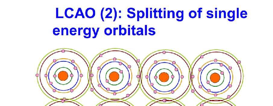
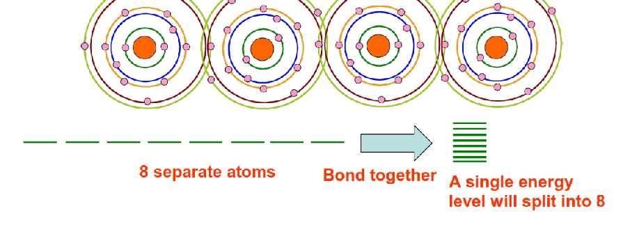
6 Discrete energy levels arise from balance of attraction force between electrons and nucleus and repulsion force between electrons each electron will have it s own energy level


7 Antisymmetric combination Symmetric combination Pauli s exclusion principle: Identical energy states split to have an energy state for each electron When two atoms brought together two distinct modes: 1- higher energy anti-bonding orbital σ* 2- lower energy bonding orbital σ
8

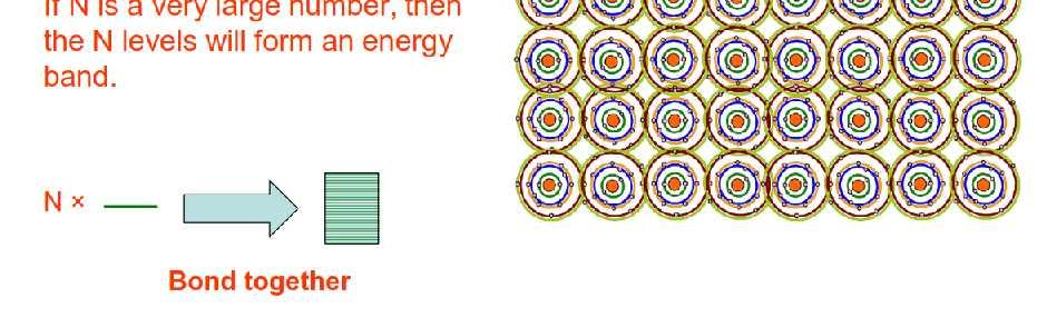
9 Energy band
10

11 Bands formation in Si

12 Bands formation in Si When atoms become close together hybridization
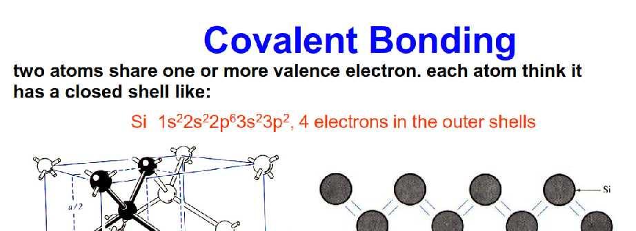
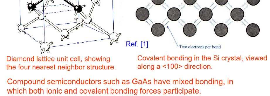
13 Bands formation in Si Figure 4: Formation of energy bands in Si when Si atoms approaches each other. (a) Si atom with 4 electrons in outer shell form (b) 4 sp 3 hybrid orbitals. (c) The hybrid orbitals form σ and σ* orbitals. (d) These orbitals overlap in a solid to form the valence and conduction band. 1st sp3 orbital in a given Si atom interacts with sp3 orbital from other Si atom. 2nd sp3 orbital the given Si atom will interact with other sp3 orbital from other second Si atom, and so on with other sp3 orbitals in the given Si atom the 4 sp3 orbitals in a given Si atoms need 4 other Si atom to form a bonded Si solid in a solid of N Si atoms, each atom is bonded to four other Si atoms. This interaction will create a band (V. B) from σ orbitals full of electrons, and other band (C.B) from σ* orbitals empty from electrons. These bands are separated by an energy gap (Eg)
14 Bands formation in Si 1) For N Si atoms, we have 14 N electrons distributed over 18 N states as shown 2) When atoms becomes close together hybridization of outer shell to sp3 orbitals 3) splitting of orbitals into valence band (4 N lower states full of electrons) and conduction band (4 N upper states empty)

15 At T = 0 K, Semiconductor has same structure as insulator filled valence band and empty conduction band no current will occur when applying E field. This is because no empty states in the valence band no net motion of electrons. The difference between insulators and Semiconductors is the Eg (for semiconducting Si Eg = 1.1 ev and for insulating diamond Eg = 5 ev). Conductivity occurs due to available states in the C.B. Insulators has a negligible no. of free electrons at room temperature almost no conductivity In metals, C.B and V.B. overlabs electrons can move freely even at 0 K


16 Electron wave function k is the propagation constant or called the wave vector Two different plots raised from plotting E and k complex 3-D surface
17 2-D draw - parabola
18
19 III-V ternary and quaternary compounds varies in composition Band structure changes change in Eg : Example GaAs doped with Al 1.83 ev As x increase all minimums moves up. But Γ minima moves up Eg still direct until reaching x=0.38 Eg becomes indirect


20 Creation of electron-hole pair (EHP) At T > 0ºK, electron are free to move in the C.B. full of empty states. In the V.B., electrons move from hole to hole holes appear to move
21
")
22 Every j electron with velocity vj have corresponding electron j with velocity -vj current density In valence band, electron move from one hole to an other hole appear to have a net motion hole current Hence, current flow in semiconductor is due to motion of charge carriers (electrons in the C.B. and holes in the V.B.)
 Electron will move from A to B gaining Kinetic energy and loosing potential energy (potential) In valence band, Hole will move opposite to electron gaining Kinetic energy and loosing")
23 E-field Electron K. E (potential) Electron will move from A to B gaining Kinetic energy and loosing potential energy (potential) In valence band, Hole will move opposite to electron gaining Kinetic energy and loosing potential energy hole K. E Under conservative force (Electric) electron will move opposite to E-field loosing potential energy and gaining kinetic energy. Hole will move with E-field loosing potential energy and gaining kinetic energy


24 (In the free space) : Electrons interact with the periodic potential of the crystal they are not completely free with
25
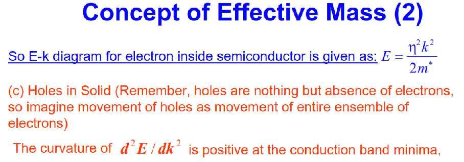
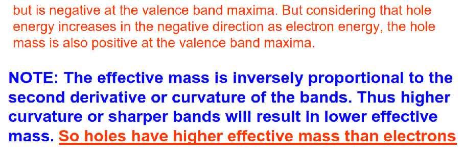
26 - hence, - m* is determined by the curvature of the E-k curve - m* is inversely proportional to the curvature mn * mp * Some effective masses in solids Ge Si 0.55 me 1.08 me 0.37 mh 0.56 mh mn* is the electron effective mass mp* is the hole effective mass me is the electron rest mass mh is the electron rest mass GaAs me 0.45 mh * For GaAs band diagram, Γ has higher curvature than L and X lower effective mass than in L and X. * Highest effective mass will be found for hole at the valence band since it has lowest curvature

27 Intrinsic Material A perfect semiconductor crystal with no impurities or lattice defects is called an Intrinsic semiconductor. In such material there are no charge carriers at 0ºK, since the valence band is filled with electrons and the conduction band is empty.
28 Intrinsic Material At T > 0 ºK at Energy enough to broke the covalent bond generation of electron hole pair (EHP); the only carriers in intrinsic semiconductor esi Eg h+ Since we have EHP electron concentration/cm3 and hole concentration/cm3 are equal and they are called intrinsic carrier concentration n = p = ni
29 Intrinsic Material EHP 3 ) If we denote the generation rate of EHPs as g i ( cm s and the recombination rate as ri ( EHP 3 ) cm s At given temperature, equilibrium requires that: ri g i Generation means creation of EHP and recombination means electron in C.B. make a transition to empty hole in the V.B. Each of these rates is temperature dependent. For example, g i (T ) increases when the temperature is raised. r n p n g 2 i r 0 0 r i i n0 and p0 are electrons and holes concentrations at equilibrium. In intrinsic material the n0 = p0 = ni with n0 p0 = n i 2 which is called the mass-action law
30 Extrinsic Material In addition to the intrinsic carriers generated thermally, it is possible to create carriers in semiconductors by purposely introducing impurities into the crystal. This process, called doping, is the most common technique for varying the conductivity of semiconductors. When a crystal is doped such that the equilibrium carrier concentrations n0 and p0 are different from the intrinsic carrier concentration ni, the material is said to be extrinsic. n0 p0 ni but still n0p0 = ni2 n-type semicondutor: doping with impurity atoms from column V donor atoms (gives extra electron in the conduction band) majority electrons and minority holes p-type semiconductor: doping with impurity atoms from column III acceptor atoms atoms (takes electron from the valence band leaving holes behind) majority holes and minority electrons

31 Extrinsic Material V P Ec Ed ººKKK 10 As Ev Sb Donor
near the conduction band so that the")
 (n0>>p0 and n0>>")
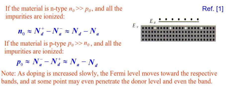
32 Donor atoms introduce donor energy levels (Ed)near the conduction band so that the electrons exited to conduction band at low temperature (about 50 ºK) (n0>>p0 and n0>> ni)

33 Extrinsic Material ш Ec B Al ººKKK 10 Ea Ev Ga In Acceptor
 near the conduction a band so that")
 leaving holes behind (p0>>n0")
34 Extrinsic Material Acceptor atoms introduce acceptor energy levels (E ) near the conduction a band so that the electrons exited from valence band at low temperature (about 50 ºK) leaving holes behind (p0>>n0 and p0>> ni)
35 Extrinsic Material e- Sb h+ Al Si
36 Extrinsic Material We can calculate the binding energy by using the Bohr model results, consider-ing the loosely bound electron as ranging about the tightly bound core electrons in a hydrogen-like orbit. 4 mq E ; n 1, K 4 0 r 2 2 2K h
37 Extrinsic Material Example: Calculate the approximate donor binding energy for Ge(εr=16, mn*=0.12m0). Answer: * n 4 mq E 2 2 8( 0 r ) h ( )( ) ( ) ( ) J eV Thus the energy to excite the donor electron from n=1 state to the free state (n= ) is 6meV.
38 Extrinsic Material Answer: * n 4 mq E 2 2 8( 0 r ) h ( )( ) ( ) ( ) J eV Thus the energy to excite the donor electron from n=1 state to the free state (n= ) is 6meV. 38
39 Carriers Concentrations In calculating semiconductor electrical properties and analyzing device behavior, it is often necessary to know the number of charge carriers per cm3 in the material. The majority carrier concentration is usually obvious in heavily doped material, since one majority carrier is obtained for each impurity atom (for the standard doping impurities). Electrons in solids obey Fermi-Dirac statistics.
40
41
42 The Fermi Level f (E f ) 1 1 e ( E f E f ) kt f(e) 1 T=0ºK T >0ºK 1>T 2 1 1/2 Ef E 42
43 The Fermi Level E f(ec) f(ec) Ec Ef [1-f(Ec)] Ev f(e) 1 1/2 0 Intrinsic p-type n-type
44 n0 = p 0
45
46
47


48 Ei is the intrinsic fermi energy level located at the middle of the energy gap
49 Electron and Hole Concentrations at Equilibrium Example 3-4: A Si sample is doped with 1017 As Atom/cm3. What is the equilibrium hole concentration p0 at 300 K? Where is EF relative to Ei? Answer: Since Nd >> ni, we can approximate n0 = Nd and ni p cm n n0 ni e ( EF Ei ) kt n EF Ei kt ln ln 0.407eV 10 ni
50 Electron and Hole Concentrations at Equilibrium Answer (Continue) : Ec EF 0.407eV 1.1eV Ei Ev 50
51 As for n0 and p0, ni is also more temperature dependent and hence is EF

52 The dependence of carrier concentration in semiconductor on temperature passes into three regimes shown in the figure
53
54
55
56
57
58
59
60
61
62
63
64
65
66
67
68
Variation of Energy Bands with Alloy Composition E
 Variation of Energy Bands with Alloy Composition E 3.0 E.8.6 L 0.3eV Al x GaAs AlAs 1- xas 1.43eV.16eV X k.4 L. X.0 X 1.8 L 1.6 1.4 0 0. 0.4 0.6 X 0.8 1 1 Carriers in intrinsic Semiconductors Ec 4º 1º
EECS130 Integrated Circuit Devices
 EECS130 Integrated Circuit Devices Professor Ali Javey 8/30/2007 Semiconductor Fundamentals Lecture 2 Read: Chapters 1 and 2 Last Lecture: Energy Band Diagram Conduction band E c E g Band gap E v Valence
Direct and Indirect Semiconductor
 Direct and Indirect Semiconductor Allowed values of energy can be plotted vs. the propagation constant, k. Since the periodicity of most lattices is different in various direction, the E-k diagram must
Lecture 7: Extrinsic semiconductors - Fermi level
 Lecture 7: Extrinsic semiconductors - Fermi level Contents 1 Dopant materials 1 2 E F in extrinsic semiconductors 5 3 Temperature dependence of carrier concentration 6 3.1 Low temperature regime (T < T
EE143 Fall 2016 Microfabrication Technologies. Evolution of Devices
 EE143 Fall 2016 Microfabrication Technologies Prof. Ming C. Wu wu@eecs.berkeley.edu 511 Sutardja Dai Hall (SDH) 1-1 Evolution of Devices Yesterday s Transistor (1947) Today s Transistor (2006) 1-2 1 Why
The Semiconductor in Equilibrium
 Lecture 6 Semiconductor physics IV The Semiconductor in Equilibrium Equilibrium, or thermal equilibrium No external forces such as voltages, electric fields. Magnetic fields, or temperature gradients are
Basic cell design. Si cell
 Basic cell design Si cell 1 Concepts needed to describe photovoltaic device 1. energy bands in semiconductors: from bonds to bands 2. free carriers: holes and electrons, doping 3. electron and hole current:
Lecture 3b. Bonding Model and Dopants. Reading: (Cont d) Notes and Anderson 2 sections
 Notes and Anderson 2 sections") Lecture 3b Bonding Model and Dopants Reading: (Cont d) Notes and Anderson 2 sections 2.3-2.7 The need for more control over carrier concentration Without help the total number of carriers (electrons and
Lecture 3b Bonding Model and Dopants Reading: (Cont d) Notes and Anderson 2 sections 2.3-2.7 The need for more control over carrier concentration Without help the total number of carriers (electrons and
Atoms? All matters on earth made of atoms (made up of elements or combination of elements).
.") Chapter 1 Atoms? All matters on earth made of atoms (made up of elements or combination of elements). Atomic Structure Atom is the smallest particle of an element that can exist in a stable or independent
Chapter 1 Atoms? All matters on earth made of atoms (made up of elements or combination of elements). Atomic Structure Atom is the smallest particle of an element that can exist in a stable or independent
SEMICONDUCTOR PHYSICS
 SEMICONDUCTOR PHYSICS by Dibyendu Chowdhury Semiconductors The materials whose electrical conductivity lies between those of conductors and insulators, are known as semiconductors. Silicon Germanium Cadmium
CHAPTER 2: ENERGY BANDS & CARRIER CONCENTRATION IN THERMAL EQUILIBRIUM. M.N.A. Halif & S.N. Sabki
 CHAPTER 2: ENERGY BANDS & CARRIER CONCENTRATION IN THERMAL EQUILIBRIUM OUTLINE 2.1 INTRODUCTION: 2.1.1 Semiconductor Materials 2.1.2 Basic Crystal Structure 2.1.3 Basic Crystal Growth technique 2.1.4 Valence
Lecture 1. OUTLINE Basic Semiconductor Physics. Reading: Chapter 2.1. Semiconductors Intrinsic (undoped) silicon Doping Carrier concentrations
 silicon Doping Carrier concentrations") Lecture 1 OUTLINE Basic Semiconductor Physics Semiconductors Intrinsic (undoped) silicon Doping Carrier concentrations Reading: Chapter 2.1 EE105 Fall 2007 Lecture 1, Slide 1 What is a Semiconductor? Low
Lecture 1 OUTLINE Basic Semiconductor Physics Semiconductors Intrinsic (undoped) silicon Doping Carrier concentrations Reading: Chapter 2.1 EE105 Fall 2007 Lecture 1, Slide 1 What is a Semiconductor? Low
Engineering 2000 Chapter 8 Semiconductors. ENG2000: R.I. Hornsey Semi: 1
 Engineering 2000 Chapter 8 Semiconductors ENG2000: R.I. Hornsey Semi: 1 Overview We need to know the electrical properties of Si To do this, we must also draw on some of the physical properties and we
MTLE-6120: Advanced Electronic Properties of Materials. Intrinsic and extrinsic semiconductors. Reading: Kasap:
 MTLE-6120: Advanced Electronic Properties of Materials 1 Intrinsic and extrinsic semiconductors Reading: Kasap: 5.1-5.6 Band structure and conduction 2 Metals: partially filled band(s) i.e. bands cross
Semiconductors 1. Explain different types of semiconductors in detail with necessary bond diagrams. Intrinsic semiconductors:
 Semiconductors 1. Explain different types of semiconductors in detail with necessary bond diagrams. There are two types of semi conductors. 1. Intrinsic semiconductors 2. Extrinsic semiconductors Intrinsic
ECE 250 Electronic Devices 1. Electronic Device Modeling
 ECE 250 Electronic Devices 1 ECE 250 Electronic Device Modeling ECE 250 Electronic Devices 2 Introduction to Semiconductor Physics You should really take a semiconductor device physics course. We can only
Lecture 2. Semiconductor Physics. Sunday 4/10/2015 Semiconductor Physics 1-1
 Lecture 2 Semiconductor Physics Sunday 4/10/2015 Semiconductor Physics 1-1 Outline Intrinsic bond model: electrons and holes Charge carrier generation and recombination Intrinsic semiconductor Doping:
ESE 372 / Spring 2013 / Lecture 5 Metal Oxide Semiconductor Field Effect Transistor
 Metal Oxide Semiconductor Field Effect Transistor V G V G 1 Metal Oxide Semiconductor Field Effect Transistor We will need to understand how this current flows through Si What is electric current? 2 Back
Lecture 2 Electrons and Holes in Semiconductors
 EE 471: Transport Phenomena in Solid State Devices Spring 2018 Lecture 2 Electrons and Holes in Semiconductors Bryan Ackland Department of Electrical and Computer Engineering Stevens Institute of Technology
EECS143 Microfabrication Technology
 EECS143 Microfabrication Technology Professor Ali Javey Introduction to Materials Lecture 1 Evolution of Devices Yesterday s Transistor (1947) Today s Transistor (2006) Why Semiconductors? Conductors e.g
Calculating Band Structure
 Calculating Band Structure Nearly free electron Assume plane wave solution for electrons Weak potential V(x) Brillouin zone edge Tight binding method Electrons in local atomic states (bound states) Interatomic
Density of states for electrons and holes. Distribution function. Conduction and valence bands
 Intrinsic Semiconductors In the field of semiconductors electrons and holes are usually referred to as free carriers, or simply carriers, because it is these particles which are responsible for carrying
n N D n p = n i p N A
 Summary of electron and hole concentration in semiconductors Intrinsic semiconductor: E G n kt i = pi = N e 2 0 Donor-doped semiconductor: n N D where N D is the concentration of donor impurity Acceptor-doped
Introduction to Engineering Materials ENGR2000. Dr.Coates
 Introduction to Engineering Materials ENGR2000 Chapter 18: Electrical Properties Dr.Coates 18.2 Ohm s Law V = IR where R is the resistance of the material, V is the voltage and I is the current. l R A
ECE 442. Spring, Lecture -2
 ECE 442 Power Semiconductor Devices and Integrated circuits Spring, 2006 University of Illinois at Chicago Lecture -2 Semiconductor physics band structures and charge carriers 1. What are the types of
electronics fundamentals
 electronics fundamentals circuits, devices, and applications THOMAS L. FLOYD DAVID M. BUCHLA Lesson 1: Diodes and Applications Semiconductors Figure 1-1 The Bohr model of an atom showing electrons in orbits
Semiconductor Physics and Devices Chapter 3.
 Introduction to the Quantum Theory of Solids We applied quantum mechanics and Schrödinger s equation to determine the behavior of electrons in a potential. Important findings Semiconductor Physics and
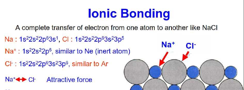
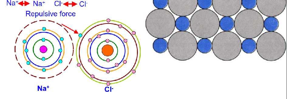
Bonding in solids The interaction of electrons in neighboring atoms of a solid serves the very important function of holding the crystal together.
 Bonding in solids The interaction of electrons in neighboring atoms of a solid serves the very important function of holding the crystal together. For example Nacl In the Nacl lattice, each Na atom is
Charge Carriers in Semiconductor
 Charge Carriers in Semiconductor To understand PN junction s IV characteristics, it is important to understand charge carriers behavior in solids, how to modify carrier densities, and different mechanisms
Three Most Important Topics (MIT) Today
 Today") Three Most Important Topics (MIT) Today Electrons in periodic potential Energy gap nearly free electron Bloch Theorem Energy gap tight binding Chapter 1 1 Electrons in Periodic Potential We now know the
Three Most Important Topics (MIT) Today Electrons in periodic potential Energy gap nearly free electron Bloch Theorem Energy gap tight binding Chapter 1 1 Electrons in Periodic Potential We now know the
Crystal Properties. MS415 Lec. 2. High performance, high current. ZnO. GaN
 Crystal Properties Crystal Lattices: Periodic arrangement of atoms Repeated unit cells (solid-state) Stuffing atoms into unit cells Determine mechanical & electrical properties High performance, high current
Note that it is traditional to draw the diagram for semiconductors rotated 90 degrees, i.e. the version on the right above.
 5 Semiconductors The nearly free electron model applies equally in the case where the Fermi level lies within a small band gap (semiconductors), as it does when the Fermi level lies within a band (metal)
Introduction to Semiconductor Physics. Prof.P. Ravindran, Department of Physics, Central University of Tamil Nadu, India
 Introduction to Semiconductor Physics 1 Prof.P. Ravindran, Department of Physics, Central University of Tamil Nadu, India http://folk.uio.no/ravi/cmp2013 Review of Semiconductor Physics Semiconductor fundamentals
CLASS 1 & 2 REVISION ON SEMICONDUCTOR PHYSICS. Reference: Electronic Devices by Floyd
 CLASS 1 & 2 REVISION ON SEMICONDUCTOR PHYSICS Reference: Electronic Devices by Floyd 1 ELECTRONIC DEVICES Diodes, transistors and integrated circuits (IC) are typical devices in electronic circuits. All
Mat E 272 Lecture 25: Electrical properties of materials
 Mat E 272 Lecture 25: Electrical properties of materials December 6, 2001 Introduction: Calcium and copper are both metals; Ca has a valence of +2 (2 electrons per atom) while Cu has a valence of +1 (1
ELECTRONIC I Lecture 1 Introduction to semiconductor. By Asst. Prof Dr. Jassim K. Hmood
 ELECTRONIC I Lecture 1 Introduction to semiconductor By Asst. Prof Dr. Jassim K. Hmood SOLID-STATE ELECTRONIC MATERIALS Electronic materials generally can be divided into three categories: insulators,
ELEMENTARY BAND THEORY
 ELEMENTARY BAND THEORY PHYSICIST Solid state band Valence band, VB Conduction band, CB Fermi energy, E F Bloch orbital, delocalized n-doping p-doping Band gap, E g Direct band gap Indirect band gap Phonon
Bohr s Model, Energy Bands, Electrons and Holes
 Dual Character of Material Particles Experimental physics before 1900 demonstrated that most of the physical phenomena can be explained by Newton's equation of motion of material particles or bodies and
Electron Energy, E E = 0. Free electron. 3s Band 2p Band Overlapping energy bands. 3p 3s 2p 2s. 2s Band. Electrons. 1s ATOM SOLID.
 Electron Energy, E Free electron Vacuum level 3p 3s 2p 2s 2s Band 3s Band 2p Band Overlapping energy bands Electrons E = 0 1s ATOM 1s SOLID In a metal the various energy bands overlap to give a single
CLASS 12th. Semiconductors
 CLASS 12th Semiconductors 01. Distinction Between Metals, Insulators and Semi-Conductors Metals are good conductors of electricity, insulators do not conduct electricity, while the semiconductors have
Semiconductors. Semiconductors also can collect and generate photons, so they are important in optoelectronic or photonic applications.
 Semiconductors Semiconducting materials have electrical properties that fall between true conductors, (like metals) which are always highly conducting and insulators (like glass or plastic or common ceramics)
Review of Semiconductor Fundamentals
 ECE 541/ME 541 Microelectronic Fabrication Techniques Review of Semiconductor Fundamentals Zheng Yang (ERF 3017, email: yangzhen@uic.edu) Page 1 Semiconductor A semiconductor is an almost insulating material,
Electrons, Holes, and Defect ionization
 Electrons, Holes, and Defect ionization The process of forming intrinsic electron-hole pairs is excitation a cross the band gap ( formation energy ). intrinsic electronic reaction : null e + h When electrons
EE 346: Semiconductor Devices
 EE 346: Semiconductor Devices Lecture - 6 02/06/2017 Tewodros A. Zewde 1 DENSTY OF STATES FUNCTON Since current is due to the flow of charge, an important step in the process is to determine the number
Chapter 12: Semiconductors
 Chapter 12: Semiconductors Bardeen & Shottky January 30, 2017 Contents 1 Band Structure 4 2 Charge Carrier Density in Intrinsic Semiconductors. 6 3 Doping of Semiconductors 12 4 Carrier Densities in Doped
Electro - Principles I
 Electro - Principles I Page 10-1 Atomic Theory It is necessary to know what goes on at the atomic level of a semiconductor so the characteristics of the semiconductor can be understood. In many cases a
EE 346: Semiconductor Devices. 02/08/2017 Tewodros A. Zewde 1
 EE 346: Semiconductor Devices 02/08/2017 Tewodros A. Zewde 1 DOPANT ATOMS AND ENERGY LEVELS Without help the total number of carriers (electrons and holes) is limited to 2ni. For most materials, this is
Semiconductors. SEM and EDAX images of an integrated circuit. SEM EDAX: Si EDAX: Al. Institut für Werkstoffe der ElektrotechnikIWE
 SEM and EDAX images of an integrated circuit SEM EDAX: Si EDAX: Al source: [Cal 99 / 605] M&D-.PPT, slide: 1, 12.02.02 Classification semiconductors electronic semiconductors mixed conductors ionic conductors
Carriers Concentration in Semiconductors - V. Prof.P. Ravindran, Department of Physics, Central University of Tamil Nadu, India
 Carriers Concentration in Semiconductors - V 1 Prof.P. Ravindran, Department of Physics, Central University of Tamil Nadu, India http://folk.uio.no/ravi/semi2013 Motion and Recombination of Electrons and
ECE 335: Electronic Engineering Lecture 2: Semiconductors
 Faculty of Engineering ECE 335: Electronic Engineering Lecture 2: Semiconductors Agenda Intrinsic Semiconductors Extrinsic Semiconductors N-type P-type Carrier Transport Drift Diffusion Semiconductors
A semiconductor is an almost insulating material, in which by contamination (doping) positive or negative charge carriers can be introduced.
 positive or negative charge carriers can be introduced.") Semiconductor A semiconductor is an almost insulating material, in which by contamination (doping) positive or negative charge carriers can be introduced. Page 2 Semiconductor materials Page 3 Energy levels
Semiconductor A semiconductor is an almost insulating material, in which by contamination (doping) positive or negative charge carriers can be introduced. Page 2 Semiconductor materials Page 3 Energy levels
First-Hand Investigation: Modeling of Semiconductors
 perform an investigation to model the behaviour of semiconductors, including the creation of a hole or positive charge on the atom that has lost the electron and the movement of electrons and holes in
Basic Semiconductor Physics
 6 Basic Semiconductor Physics 6.1 Introduction With this chapter we start with the discussion of some important concepts from semiconductor physics, which are required to understand the operation of solar
From Last Time Important new Quantum Mechanical Concepts. Atoms and Molecules. Today. Symmetry. Simple molecules.
 Today From Last Time Important new Quantum Mechanical Concepts Indistinguishability: Symmetries of the wavefunction: Symmetric and Antisymmetric Pauli exclusion principle: only one fermion per state Spin
Lecture 2 - Carrier Statistics in Equilibrium. September 5, 2002
 6.720J/3.43J Integrated Microelectronic Devices Fall 2002 Lecture 21 Lecture 2 Carrier Statistics in Equilibrium Contents: September 5, 2002 1. Conduction and valence bands, bandgap, holes 2. Intrinsic
Key Questions. ECE 340 Lecture 6 : Intrinsic and Extrinsic Material I 9/10/12. Class Outline: Effective Mass Intrinsic Material
 9/1/1 ECE 34 Lecture 6 : Intrinsic and Extrinsic Material I Class Outline: Things you should know when you leave Key Questions What is the physical meaning of the effective mass What does a negative effective
Due to the quantum nature of electrons, one energy state can be occupied only by one electron.
 In crystalline solids, not all values of the electron energy are possible. The allowed intervals of energy are called allowed bands (shown as blue and chess-board blue). The forbidden intervals are called
ENERGY BANDS AND GAPS IN SEMICONDUCTOR. Muhammad Hafeez Javed
 ENERGY BANDS AND GAPS IN SEMICONDUCTOR Muhammad Hafeez Javed www.rmhjaved.com rmhjaved@gmail.com Out Line Introduction Energy band Classification of materials Direct and indirect band gap of SC Classification
Solid State Device Fundamentals
 4. lectrons and Holes Solid State Device Fundamentals NS 45 Lecture Course by Alexander M. Zaitsev alexander.zaitsev@csi.cuny.edu Tel: 718 982 2812 4N101b 1 4. lectrons and Holes Free electrons and holes
EE 346: Semiconductor Devices
 EE 346: Semiconductor Devices Lecture - 5 02/01/2017 Tewodros A. Zewde 1 The One-Electron Atom The potential function is due to the coulomb attraction between the proton and electron and is given by where
Chemistry Instrumental Analysis Lecture 8. Chem 4631
 Chemistry 4631 Instrumental Analysis Lecture 8 UV to IR Components of Optical Basic components of spectroscopic instruments: stable source of radiant energy transparent container to hold sample device
Chapter 1 Overview of Semiconductor Materials and Physics
 Chapter 1 Overview of Semiconductor Materials and Physics Professor Paul K. Chu Conductivity / Resistivity of Insulators, Semiconductors, and Conductors Semiconductor Elements Period II III IV V VI 2 B
smal band gap Saturday, April 9, 2011
 small band gap upper (conduction) band empty small gap valence band filled 2s 2p 2s 2p hybrid (s+p)band 2p no gap 2s (depend on the crystallographic orientation) extrinsic semiconductor semi-metal electron
Semiconductor Physics
 Semiconductor Physics Motivation Is it possible that there might be current flowing in a conductor (or a semiconductor) even when there is no potential difference supplied across its ends? Look at the
Unit IV Semiconductors Engineering Physics
 Introduction A semiconductor is a material that has a resistivity lies between that of a conductor and an insulator. The conductivity of a semiconductor material can be varied under an external electrical
Electronic Circuits for Mechatronics ELCT 609 Lecture 2: PN Junctions (1)
") Electronic Circuits for Mechatronics ELCT 609 Lecture 2: PN Junctions (1) Assistant Professor Office: C3.315 E-mail: eman.azab@guc.edu.eg 1 Electronic (Semiconductor) Devices P-N Junctions (Diodes): Physical
Electronic Circuits for Mechatronics ELCT 609 Lecture 2: PN Junctions (1) Assistant Professor Office: C3.315 E-mail: eman.azab@guc.edu.eg 1 Electronic (Semiconductor) Devices P-N Junctions (Diodes): Physical
Chapter Two. Energy Bands and Effective Mass
 Chapter Two Energy Bands and Effective Mass Energy Bands Formation At Low Temperature At Room Temperature Valence Band Insulators Metals Effective Mass Energy-Momentum Diagrams Direct and Indirect Semiconduction
EE495/695 Introduction to Semiconductors I. Y. Baghzouz ECE Department UNLV
 EE495/695 Introduction to Semiconductors I Y. Baghzouz ECE Department UNLV Introduction Solar cells have always been aligned closely with other electronic devices. We will cover the basic aspects of semiconductor
Energy bands in solids. Some pictures are taken from Ashcroft and Mermin from Kittel from Mizutani and from several sources on the web.
 Energy bands in solids Some pictures are taken from Ashcroft and Mermin from Kittel from Mizutani and from several sources on the web. we are starting to remind p E = = mv 1 2 = k mv = 2 2 k 2m 2 Some
ELEC311( 물리전자, Physical Electronics) Course Outlines:
 Course Outlines:") ELEC311( 물리전자, Physical Electronics) Course Outlines: by Professor Jung-Hee Lee Lecture notes are prepared with PPT and available before the class (http://abeek.knu.ac.kr). The topics in the notes are
ELEC311( 물리전자, Physical Electronics) Course Outlines: by Professor Jung-Hee Lee Lecture notes are prepared with PPT and available before the class (http://abeek.knu.ac.kr). The topics in the notes are
ECE 340 Lecture 6 : Intrinsic and Extrinsic Material I Class Outline:
 ECE 340 Lecture 6 : Intrinsic and Extrinsic Material I Class Outline: Effective Mass Intrinsic Material Extrinsic Material Things you should know when you leave Key Questions What is the physical meaning
Semiconductor physics I. The Crystal Structure of Solids
 Lecture 3 Semiconductor physics I The Crystal Structure of Solids 1 Semiconductor materials Types of solids Space lattices Atomic Bonding Imperfection and doping in SOLIDS 2 Semiconductor Semiconductors
Lecture 02 Semiconductor Physics
 Lecture 02 Semiconductor Physics Prepared By Dr. Eng. Sherif Hekal Assistant Professor, CCE department Lecture 02 Semiconductors 10/15/201 7 1 ILOS In this section, we will learn: The basic properties
Chapter 2. Semiconductor Fundamentals
 hapter Semiconductor Fundamentals.0 Introduction There are altogether 9 types of natural occurring elements, of which only few types are important in semiconductor physics and technology. They are the
Course overview. Me: Dr Luke Wilson. The course: Physics and applications of semiconductors. Office: E17 open door policy
 Course overview Me: Dr Luke Wilson Office: E17 open door policy email: luke.wilson@sheffield.ac.uk The course: Physics and applications of semiconductors 10 lectures aim is to allow time for at least one
* motif: a single or repeated design or color
 Chapter 2. Structure A. Electronic structure vs. Geometric structure B. Clean surface vs. Adsorbate covered surface (substrate + overlayer) C. Adsorbate structure - how are the adsorbed molecules bound
半導體元件與物理. Semiconductor Devices and physics 許正興國立聯合大學電機工程學系 聯大電機系電子材料與元件應用實驗室
 半導體元件與物理 Semiconductor Devices and physics 許正興國立聯合大學電機工程學系 1. Crystal Structure of Solids 2. Quantum Theory of Solids 3. Semiconductor in Equilibrium and Carrier Transport phenomena 4. PN Junction and
The photovoltaic effect occurs in semiconductors where there are distinct valence and
 How a Photovoltaic Cell Works The photovoltaic effect occurs in semiconductors where there are distinct valence and conduction bands. (There are energies at which electrons can not exist within the solid)
LN 3 IDLE MIND SOLUTIONS
 IDLE MIND SOLUTIONS 1. Let us first look in most general terms at the optical properties of solids with band gaps (E g ) of less than 4 ev, semiconductors by definition. The band gap energy (E g ) can
Solid State Device Fundamentals
 Solid State Device Fundamentals ES 345 Lecture Course by Alexander M. Zaitsev alexander.zaitsev@csi.cuny.edu Tel: 718 982 2812 Oice 4101b 1 The ree electron model o metals The ree electron model o metals
EXTRINSIC SEMICONDUCTOR
 EXTRINSIC SEMICONDUCTOR EXTRINSIC SEMICONDUCTOR A semiconductor in which the impurity atoms are added by doping process is called Extrinsic semiconductor. The addition of impurities increases the carrier
Concept of Semiconductor Physics
 Concept of Semiconductor Physics Prof. (Dr.) Pradeep Kumar Sharma Department of Physics University of Engineering & Management, Jaipur OBJECTIVES: This course deals with an introduction to semiconductor
Electronic PRINCIPLES
 MALVINO & BATES Electronic PRINCIPLES SEVENTH EDITION Chapter 2 Semiconductors Topics Covered in Chapter 2 Conductors Semiconductors Silicon crystals Intrinsic semiconductors Two types of flow Doping a
Semiconductor Device Physics
 1 Semiconductor Device Physics Lecture 1 http://zitompul.wordpress.com 2 0 1 3 2 Semiconductor Device Physics Textbook: Semiconductor Device Fundamentals, Robert F. Pierret, International Edition, Addison
CME 300 Properties of Materials. ANSWERS: Homework 9 November 26, As atoms approach each other in the solid state the quantized energy states:
 CME 300 Properties of Materials ANSWERS: Homework 9 November 26, 2011 As atoms approach each other in the solid state the quantized energy states: are split. This splitting is associated with the wave
Diamond. Covalent Insulators and Semiconductors. Silicon, Germanium, Gray Tin. Chem 462 September 24, 2004
 Covalent Insulators and Chem 462 September 24, 2004 Diamond Pure sp 3 carbon All bonds staggered- ideal d(c-c) - 1.54 Å, like ethane Silicon, Germanium, Gray Tin Diamond structure Si and Ge: semiconductors
PH575 Spring Lecture #19 Semiconductors: electrical & optical properties: Kittel Ch. 8 pp ; Ch. 20
 PH575 Spring 2014 Lecture #19 Semiconductors: electrical & optical properties: Kittel Ch. 8 pp. 205-214; Ch. 20 Simplified diagram of the filling of electronic band structure in various types of material,
Topic 11-3: Fermi Levels of Intrinsic Semiconductors with Effective Mass in Temperature
 Topic 11-3: Fermi Levels of Intrinsic Semiconductors with Effective Mass in Temperature Summary: In this video we aim to get an expression for carrier concentration in an intrinsic semiconductor. To do
PHYS208 P-N Junction. Olav Torheim. May 30, 2007
 1 PHYS208 P-N Junction Olav Torheim May 30, 2007 1 Intrinsic semiconductors The lower end of the conduction band is a parabola, just like in the quadratic free electron case (E = h2 k 2 2m ). The density
Electrons in materials. (where are they, what is their energy)
") Electrons in materials (where are they, what is their energy) 1 Lone atoms A single atom has electrons in shells and sub shells. Each of these have a distinct energy level. The diagram shows an example
Electrons in materials (where are they, what is their energy) 1 Lone atoms A single atom has electrons in shells and sub shells. Each of these have a distinct energy level. The diagram shows an example
Free Electron Model for Metals
 Free Electron Model for Metals Metals are very good at conducting both heat and electricity. A lattice of in a sea of electrons shared between all nuclei (moving freely between them): This is referred
Lecture 2 - Carrier Statistics in Equilibrium. February 8, 2007
 6.720J/3.43J Integrated Microelectronic Devices Spring 2007 Lecture 21 Lecture 2 Carrier Statistics in Equilibrium Contents: February 8, 2007 1. Conduction and valence bands, bandgap, holes 2. Intrinsic
3.1 Introduction to Semiconductors. Y. Baghzouz ECE Department UNLV
 3.1 Introduction to Semiconductors Y. Baghzouz ECE Department UNLV Introduction In this lecture, we will cover the basic aspects of semiconductor materials, and the physical mechanisms which are at the
Semiconductor Physics. Lecture 3
 Semiconductor Physics Lecture 3 Intrinsic carrier density Intrinsic carrier density Law of mass action Valid also if we add an impurity which either donates extra electrons or holes the number of carriers
Solid State Electronics EC210 Arab Academy for Science and Technology AAST Cairo Fall Lecture 10: Semiconductors
 Solid State Electronics EC210 Arab Academy for Science and Technology AAST Cairo Fall 2014 Lecture 10: Semiconductors Lecture Notes Prepared by: Dr. Amr Bayoumi, Dr. Nadia Rafat These PowerPoint color
UNIVERSITY OF CALIFORNIA College of Engineering Department of Electrical Engineering and Computer Sciences. EECS 130 Professor Ali Javey Fall 2006
 UNIVERSITY OF CALIFORNIA College of Engineering Department of Electrical Engineering and Computer Sciences EECS 130 Professor Ali Javey Fall 2006 Midterm I Name: Closed book. One sheet of notes is allowed.
Chem 241. Lecture 24. UMass Amherst Biochemistry... Teaching Initiative
 Chem 241 Lecture 24 UMass Amherst Biochemistry... Teaching Initiative Announcement Mistake we have class on the 3 rd not 4 th Exam 3 Originally scheduled April 23 rd (Friday) What about April 26 th (Next
I. Introduction II. Solid State Physics Detection of Light Bernhard Brandl 1
 Detection of Light I. Introduction II. Solid State Physics 4-2-2015 Detection of Light Bernhard Brandl 1 4-2-2015 Detection of Light Bernhard Brandl 2 Blabla Recommended 4-2-2015 Detection of Light Bernhard
ITT Technical Institute ET215 Devices I Unit 1
 ITT Technical Institute ET215 Devices I Unit 1 Chapter 1 Chapter 2, Sections 2.1-2.4 Chapter 1 Basic Concepts of Analog Circuits Recall ET115 & ET145 Ohms Law I = V/R If voltage across a resistor increases
Solid State Device Fundamentals
 Solid State Device Fundamentals ENS 345 Lecture Course by Alexander M. Zaitsev alexander.zaitsev@csi.cuny.edu Tel: 718 982 2812 Office 4N101b 1 The free electron model of metals The free electron model