ME 4875/MTE C/16. Introduction to Nanomaterials and Nanotechnology. Lecture 1 - Introduction
|
|
|
- Russell Harvey
- 6 years ago
- Views:
Transcription


1 ME 4875/MTE C/16 Introduction to Nanomaterials and Nanotechnology Lecture 1 - Introduction 1
2 Course Information Syllabus uploaded to mywpi Schedule: Lectures MT-RF 2:00-2:50 pm in Salisbury Labs 411 Contact Information: Prof. Pratap Rao , HL 106 TA - Xuejian Lv xlv@wpi.edu Office Hours: Prof. Rao M,T,R,F 3-4pm, HL 106 TA To be determined 2
3 Course Information Objective of the course: Lectures and homework: Broad introduction to nanomaterials and nanotechnology, inspire you to look into these topics further Project: More in-depth study of a chosen topic area No textbook, just lecture slides and assigned readings Coursework and Grading: 4 Homework Sets* 60% *Students who are registered for graduate course MTE 575 will have additional homework problems assigned Project (Report + Poster Presentation) 40% Students will work in 4-person teams on the course project. Students are responsible for printing their posters and bearing the printing costs. 3
4 Course Information Waitlisted students: See me after class Deadline conflicts: Inform me during the first week of the term of any commitments (religious observances, WPI sports, etc.) or circumstances that might affect your ability to meet any of the deadlines in the course. Student Accommodations: If you need course adaptations or accommodations because of a disability, or if you have medical information to share with me, please make an appointment with me as soon as possible. If you have not already done so, students with disabilities who believe that they may need accommodations in this class are encouraged to contact the Office of Disability Services(ODS) [124 Daniels Hall, disabilityservices@wpi.edu, (508) ] as soon as possible to ensure that such accommodations are implemented in a timely fashion. 4
5 Immediate Assignments Lecture Slides posted under Course Materials > Lecture Slides Reading Assignments posted under Course Materials > Reading Assignments HW 1 posted on mywpi under Assignments due in class Friday January 22 5
6 Outline What is nanotechnology? Why nano? History of nanotechnology 6


7 The National Science Foundation defines nanotechnology as research and development at the atomic/molecular/macromolecular level length scale of approximately nanometers fundamental understanding of phenomena at the nanoscale structures, devices and systems that have novel properties and functions because of their small size. Nanotechnology overlaps with the other sciences (physics, chemistry, biology, materials) and engineering. Earth = 1 m Definition of Nanotechnology 1 meter = 10 9 nanometer Baseball = 1 nm If the earth were shrunk down to 1 m diameter. a baseball would be 1 nm in diameter 7


 (1/1000")
 1 nm")

8 Length Scale of Nanotechnology optical microscope electron microscope naked eye individual carbon atoms! millimeter (mm) (1/1000 meter) micrometer (μm) (1/1000 millimeter) 1 nm atoms, molecules, DNA new physical phenomena nanometer (nm) (1/1000 micrometer) 8

 devices 10-100 mm wide Human hair ~ 60-120 mm wide Red blood")
 Pollen grain Red blood cells Intel Transistor Feature")


9 Soft x-ray Nanoworld Microworld Ultraviolet Visible Infrared Microwave The Scale of Things Nanometers and More Things Natural 10-2 m 1 cm 10 mm Things Manmade Head of a pin 1-2 mm Ant ~ 5 mm 10-3 m 1,000,000 nanometers = 1 millimeter (mm) Dust mite 200 mm 10-4 m 0.1 mm 100 mm MicroElectroMechanical (MEMS) devices mm wide Human hair ~ mm wide Red blood cells (~7-8 mm) Fly ash ~ mm 10-5 m 10-6 m 0.01 mm 10 mm 1,000 nanometers = 1 micrometer (mm) Pollen grain Red blood cells Intel Transistor Feature size 22 nm 10-7 m 0.1 mm 100 nm ~10 nm diameter ATP synthase 10-8 m 0.01 mm 10 nm Self-assembled, Nature-inspired structure Many 10s of nm Nanotube electrode DNA ~2-1/2 nm diameter Atoms of silicon spacing nm 10-9 m m 1 nanometer (nm) 0.1 nm Quantum corral of 48 iron atoms on copper surface positioned one at a time with an STM tip Corral diameter 14 nm Carbon Bucky ball ~1 nm diameter Carbon nanotube ~1.3 nm diameter 9 Office of Basic Energy Sciences Office of Science, U.S. DOE Version , pmd
10 Course Outline Week 1-2 Introduction to Nanomaterials and Nanotechnology Project topics and resources Atoms, molecules and crystals (briefly) Nanotechnology Characterization of materials at the nanoscale Synthesis of materials at the nanoscale Physical phenomena at the nanoscale with examples and applications Week 2-3 Weeks 3-5 Weeks 5-7 Week 7 Poster presentations more in-depth study of one application of nanotechnology per group 10
11 Why Nano? Physical properties The physical properties of nanoscale materials depend on their size (materials can have tunable properties at the nanoscale). Enhanced and/or novel phenomena unique to small structures. Gravitational forces become negligible while electromagnetic forces, quantum mechanical effects, and surface phenomena dominate. Relevant device limit. In both synthetic and natural systems, the nanometer scale represents a limit to which most functional structures might be scaled. Unexpected science & technology. The multi-/interdisciplinary nature of nanoscience working at interface between and bringing together different fields could lead to revolutionary advances. 11

12 Why Nano? Scaling of Surface Area with Size Consider a cube: Surface Area Volume S = 6a 2 V = a 3 nano.gov Surface Area/Volume S V = 6 a In many cases, useful region is only at the surface By using nano-scale size, we can make all the material useful useful region wasted region macro-scale nano-scale


13 High Surface Area Nanostructures in Nature - Gecko s Foot Gecko s Foot The extremely high surface area of a Gecko s foot means that even the weak Van der Waals force can allow the Gecko to walk on the ceiling! > few nanometers no force few nanometers Van der Waals force


14 High Surface Area Nanostructures in Nature - Animal Lung Smaller alveolar diameter leads to more efficient oxygen transfer for the same mass of lung! 14


15 Why Nano? Quantum effects Efficient charge and mass transport 1.7 nm Donega, Chem. Soc. Rev., nm Li+ Enhanced Strength Schwierz, Nature Nanotechnology, 2010 Surface/Interface effects smooth nanowires rough nanowires 10 μm Wu et al., Nature Materials, nm Hochbaum et al. Nature,


16 Natural Multiscale Hierarchical Materials Scale of biology Sea Sponge Skeleton Hemoglobin: 5.5 nm; DNA: 2nm 1 cm 5 mm 100 μm nano-micro micro-milli milli-centi 5 μm 500 nm 10 μm Lotus Leaf Aizenberg et al. Science, 2005 Stratakis et al. SPIE Newsroom, 2005 cell tissue organ Gecko s Foot Karp et al. MIT 16

 for")

 (Lux Research, 2010) Theis et al.")
17 Why Nano? Commercial products involving nanotechnology Computer chips Inkjet Printer heads Gyroscopes Sunscreen Catalysts ipod Nano HEAD Nano Ti Giant Magnetoresistance (GMR) for high density information storage. Nobel Prize in Physics 2007 for discovery of GMR in 1988 Global economy for Nano: $251 billion (2009), $2.4 trillion (2015) (Lux Research, 2010) Theis et al., Nature Nanotech. (2006),

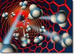
18 History of Nanotechnology Richard Feynman s seminal lecture There s Plenty of Room at the Bottom Norio Taniguchi of the Tokyo University of Science was the first to use the term "nano-technology" in a 1974 conference to describe material addition or removal processes such as thin film deposition and ion beam milling exhibiting characteristic control on the order of a nanometer K. Eric Drexler introduces idea of a molecular assembler, a hypothetical machine which would manufacture molecules and molecular devices atom-by-atom Invention of Scanning Tunneling Microscope (1986 Nobel Prize in Physics) Richard Smalley, Robert Curl and Harold Kroto discover C 60 molecule (1996 Nobel Prize in Chemistry), one of the first nanometer-sized molecules, and closely related to carbon nanotubes 18
. 2.")

19 History of Nanotechnology Feynman Prizes (1959) Richard Feynman offered $1000 to anyone who could: 1. Build a motor that would fit inside a 1/64 x1/64 x1/64 box (400mm). 2. Write a page of text with letters that are small enough for the Encyclopedia Britannica to be printed on a pin head. First Feynman Prize William McLellan made a small motor almost immediately using an optical microscope, toothpick, and watchmaker's lathe. 19
 used")

20 History of Nanotechnology Second Feynman Prize 1985: Tom Newman, Fabian Pease (Stanford University) used e-beam lithography to write part of A Tale of Two Cities at the length scale requested by Feynman. 25 nm linewidth 20

21 History of Nanotechnology Scanning Tunneling Microscopy (STM) 21
22 Two Paradigms for Synthesis of Nanomaterials and Devices Top-down Bottom-up Bulk Atomic or molecular precursors Lithography Nanosynthesis Nanostructures Nanostructures Domain of Engineering Domain of Chemistry 22
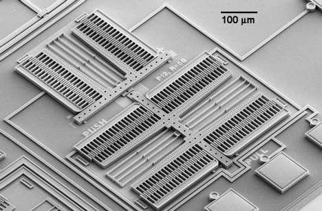
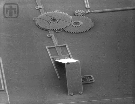
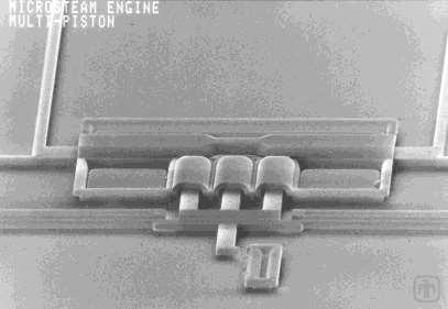
23 Top Down MicroElectroMechanical Systems (MEMS) comb drive hinged mirror steam engine tissue shredder 23


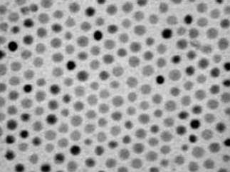
24 Bottom-Up Nanomaterials Dots Rods Tetrapods 50 nm Carbon Nanotubes Ordered Arrays of Nanowires Assembly of Nanospheres These nano-components could be the building blocks of useful nanomaterials and devices 24
 Scanning")

 Many other")

25 Imaging of Nanomaterials Optical Microscope (>100 nm) Scanning Electron Microscope (few nm) Transmission Electron Microscope (1/10 nm) Scanning Tunneling Microscope (1/100 nm) Many other types of characterization, too (chemical, crystallographic, electrical, etc.) 25
26 Tomorrow More on applications of nanotechnology More on project 26
27 Immediate Assignments Lecture Slides posted under Course Materials > Lecture Slides Reading Assignments posted under Course Materials > Reading Assignments HW 1 posted on mywpi under Assignments due in class Friday January 22 27
28 Waitlisted Students If you are a graduate student, please print and bring me an add/drop form (available from the registrar s website), and I will sign it for you to register for the class If you are an undergraduate student, fill out an index card: Name Major Undergrad year (fresh, soph, junior, senior) Reasons why you need to take this class THIS term I will you to let you know if you can or can t register If I you to say you can register, please print and bring me an add/drop form (available from the registrar s website), and I will sign it for you to register for the class You can access the course materials at nanoenergy.wpi.edu until you get access to the mywpi site 28
ME 4875/MTE C/18. Introduction to Nanomaterials and Nanotechnology. Lecture 1 - Introduction
 ME 4875/MTE 575 - C/18 Introduction to Nanomaterials and Nanotechnology Lecture 1 - Introduction 1 Course Information Syllabus uploaded to Canvas Schedule: Lectures MT-RF 10:00-10:50 pm in Olin Hall 223
PV Tutorial Allen Hermann, Ph. D. Professor of Physics Emeritus, and Professor of Music Adjunct, University of Colorado, Boulder, Colorado, USA and
 PV Tutorial Allen Hermann, Ph. D. Professor of Physics Emeritus, and Professor of Music Adjunct, University of Colorado, Boulder, Colorado, USA and Vice-president, NanoTech Inc. Lexington, Kentucky, USA
672 Advanced Solid State Physics. Scanning Tunneling Microscopy
 672 Advanced Solid State Physics Scanning Tunneling Microscopy Biao Hu Outline: 1. Introduction to STM 2. STM principle & working modes 3. STM application & extension 4. STM in our group 1. Introduction
Nanotechnology. Gavin Lawes Department of Physics and Astronomy
 Nanotechnology Gavin Lawes Department of Physics and Astronomy Earth-Moon distance 4x10 8 m (courtesy NASA) Length scales (Part I) Person 2m Magnetic nanoparticle 5x10⁻⁹ m 10 10 m 10 5 m 1 m 10-5 m 10-10
ME 4875/MTE C16. Introduction to Nanomaterials and Nanotechnology. Lecture 2 - Applications of Nanomaterials + Projects
 ME 4875/MTE 575 - C16 Introduction to Nanomaterials and Nanotechnology Lecture 2 - Applications of Nanomaterials + Projects 1 Project Teams of 4 students each Literature review of one application of nanotechnology
Nanotechnology Fabrication Methods.
 Nanotechnology Fabrication Methods. 10 / 05 / 2016 1 Summary: 1.Introduction to Nanotechnology:...3 2.Nanotechnology Fabrication Methods:...5 2.1.Top-down Methods:...7 2.2.Bottom-up Methods:...16 3.Conclusions:...19
29: Nanotechnology. What is Nanotechnology? Properties Control and Understanding. Nanomaterials
 29: Nanotechnology What is Nanotechnology? Properties Control and Understanding Nanomaterials Making nanomaterials Seeing at the nanoscale Quantum Dots Carbon Nanotubes Biology at the Nanoscale Some Applications
PHY313 - CEI544 The Mystery of Matter From Quarks to the Cosmos Fall 2005
 PHY313 - CEI544 The Mystery of Matter From Quarks to the Cosmos Fall 2005 Peter Paul Office Physics D-143 www.physics.sunysb.edu then click on PHY313 or CEI544 Peter Paul 09/1/05 PHY313-CEI544 Fall-05
Nanomaterials and their Optical Applications
 Nanomaterials and their Optical Applications Winter Semester 2013 Lecture 02 rachel.grange@uni-jena.de http://www.iap.uni-jena.de/multiphoton Lecture 2: outline 2 Introduction to Nanophotonics Theoretical
Nanotechnology. Yung Liou P601 Institute of Physics Academia Sinica
 Nanotechnology Yung Liou P601 yung@phys.sinica.edu.tw Institute of Physics Academia Sinica 1 1st week Definition of Nanotechnology The Interagency Subcommittee on Nanoscale Science, Engineering and Technology
Materials. Definitions of nanotechnology. The term nanotechnology was invented by Professor Norio Taniguchi at the University of Tokyo in 1971.
 Materials Definitions of nanotechnology The term nanotechnology was invented by Professor Norio Taniguchi at the University of Tokyo in 1971. The original definition, translated into English Nano-technology'
There s plenty of room at the bottom! - R.P. Feynman, Nanostructure: a piece of material with at least one dimension less than 100 nm in extent.
 Nanostructures and Nanotechnology There s plenty of room at the bottom! - R.P. Feynman, 1959 Materials behave differently when structured at the nm scale than they do in bulk. Technologies now exist that
CSCI 2570 Introduction to Nanocomputing
 CSCI 2570 Introduction to Nanocomputing The Emergence of Nanotechnology John E Savage Purpose of the Course The end of Moore s Law is in sight. Researchers are now exploring replacements for standard methods
26.542: COLLOIDAL NANOSCIENCE & NANOSCALE ENGINEERING Fall 2013
 26.542: COLLOIDAL NANOSCIENCE & NANOSCALE ENGINEERING Fall 2013 Classes: Thurs, 6-9 pm; Ball Hall Room 208 Professor: Dr. B. Budhlall Office: Ball Hall 203B, Phone: 978-934-3414 Email: Bridgette_Budhlall@uml.edu
In the name of Allah
 In the name of Allah Nano chemistry- 4 th stage Lecture No. 1 History of nanotechnology 16-10-2016 Assistance prof. Dr. Luma Majeed Ahmed lumamajeed2013@gmail.com, luma.ahmed@uokerbala.edu.iq Nano chemistry-4
CHEM 6342 Nanotechnology Fundamentals and Applications. Dieter Cremer, 325 FOSC, ext ,
 D. Cremer, CHEM 6342, Nanotechnology - Fundamentals and Applications 1 CHEM 6342 Nanotechnology Fundamentals and Applications Class location: Lectures, time and location: Lab times and location: Instructor:
Like space travel and the Internet before it, the possibilities of the nano world catches the imagination of school children and scientists alike.
 The Nano World Preface Nano is the cool thing and it s the buzzword Like space travel and the Internet before it, the possibilities of the nano world catches the imagination of school children and scientists
MRSEC. Refrigerator Magnet Activity Guide. Quick Reference Activity Guide. a) b) c) = north = south. Activity Materials
 b) c) = north = south. Activity Materials") MRSEC Refrigerator Magnet Activity Guide Quick Reference Activity Guide Activity Materials Refrigerator magnet with removable probe strip Magnetic field diagrams Starting Points One of the great breakthroughs
MRSEC Refrigerator Magnet Activity Guide Quick Reference Activity Guide Activity Materials Refrigerator magnet with removable probe strip Magnetic field diagrams Starting Points One of the great breakthroughs
Nanotubes and Nanowires - One-dimensional Materials
 NCLT July 13th, 2006 Nanotubes and Nanowires - One-dimensional Materials Tim Sands Materials Engineering and Electrical & Computer Engineering Birck Nanotechnology Center Purdue University 100 nm Si/SiGe
Lesson 4: Tools of the Nanosciences. Student Materials
 Lesson 4: Tools of the Nanosciences Student Materials Contents Black Box Lab Activity: Student Instructions and Worksheet Seeing and Building Small Things: Student Reading Seeing and Building Small Things:
Nanotechnology where size matters
 Nanotechnology where size matters J Emyr Macdonald Overview Ways of seeing very small things What is nanotechnology and why is it important? Building nanostructures What we can do with nanotechnology?
Welcome to Physics 161 Elements of Physics Fall 2018, Sept 4. Wim Kloet
 Welcome to Physics 161 Elements of Physics Fall 2018, Sept 4 Wim Kloet 1 Lecture 1 TOPICS Administration - course web page - contact details Course materials - text book - iclicker - syllabus Course Components
Nanotechnology. An Introduction
 Nanotechnology An Introduction Nanotechnology A new interdisciplinary field of science The study of systems at the nanoscale The use of tools at the nanoscale Building and applying structures that are
CH676 Physical Chemistry: Principles and Applications. CH676 Physical Chemistry: Principles and Applications
 CH676 Physical Chemistry: Principles and Applications History of Nanotechnology: Time Line Democritus in ancient Greece: concept of atom 1900 : Rutherford : discovery of atomic nucleus The first TEM was
STATISTICAL AND THERMAL PHYSICS
 Phys 362 Spring 2015 STATISTICAL AND THERMAL PHYSICS Phys 362 Spring 2015 Instructor: Office: Professor David Collins WS 228B Phone: 248-1787 email: Office Hours: dacollin@coloradomesa.edu M 9 10 am, 11
LECTURE 1 : INTRODUCTION TO NANOMECHANICS
 I LECTURE 1 : INTRODUCTION TO NANOMECHANICS Outline : NANOTECHNOLOGY / NANOMECHANICS DEFINITIONS... 2 WHY IS NANO INTERESTING?... 3 HISTORY OF NANOTECHNOLOGY/NANOMECHANICS : TIME LINE... 4 The First Talk
There's Plenty of Room at the Bottom
 There's Plenty of Room at the Bottom 12/29/1959 Feynman asked why not put the entire Encyclopedia Britannica (24 volumes) on a pin head (requires atomic scale recording). He proposed to use electron microscope
MCC026:Nanoscience. at the border between chemistry and physics. Samuel Lara-Avila
 MCC026:Nanoscience at the border between chemistry and physics Samuel Lara-Avila Quantum Device Physics Lab Department of Microtechnology and Nanoscience (MC2) November, 2016 Nanoscience Femto 10-15 Nano:
QUEENSBOROUGH COMMUNITY COLLEGE CHEMISTRY DEPARTMENT. LECTURE: 3 hours per week CREDITS: 3
 QUEENSBOROUGH COMMUNITY COLLEGE CHEMISTRY DEPARTMENT CH-5 H INTRODUCTION TO NANOSCIENCE LECTURE: hours per week CREDITS: TEXTBOOK: Introduction to Nanoscience & Nanotechnology. ISBN: 978-400-4779-0 By
SYLLABUS FINDING NANO Syllabus NanoSCI DISCOVERING NANOTECHNOLOGY AND CULTURE IN GERMANY
 1. Syllabus NanoSCI Course title: NanoSCI - Electronic Properties of Nanoengineered Materials Catalog description: Physics and technology of nanoengineered materials and devices. Semiconductor nanostructures.
Chapter 10. Nanometrology. Oxford University Press All rights reserved.
 Chapter 10 Nanometrology Oxford University Press 2013. All rights reserved. 1 Introduction Nanometrology is the science of measurement at the nanoscale level. Figure illustrates where nanoscale stands
There s still plenty of room at the bottom
 There s still plenty of room at the bottom Foundations of the nanotechnology revolution Ross Lockwood Department of Physics February 4, 2014 Richard Feynman Born May 11th, 1918, in Far Rockaway, New York
Chapter 12. Nanometrology. Oxford University Press All rights reserved.
 Chapter 12 Nanometrology Introduction Nanometrology is the science of measurement at the nanoscale level. Figure illustrates where nanoscale stands in relation to a meter and sub divisions of meter. Nanometrology
National Science and Technology Council (NSTC) Committee on Technology
 Committee on Technology") BY LYNN YARRIS "The emerging fields of nanoscience and nanoengineering are leading to unprecedented understanding and control over the fundamental building blocks of all physical things. This is likely
BY LYNN YARRIS "The emerging fields of nanoscience and nanoengineering are leading to unprecedented understanding and control over the fundamental building blocks of all physical things. This is likely
From nanophysics research labs to cell phones. Dr. András Halbritter Department of Physics associate professor
 From nanophysics research labs to cell phones Dr. András Halbritter Department of Physics associate professor Curriculum Vitae Birth: 1976. High-school graduation: 1994. Master degree: 1999. PhD: 2003.
CH676 Physical Chemistry: Principles and Applications. CH676 Physical Chemistry: Principles and Applications
 CH676 Physical Chemistry: Principles and Applications Contact Information Professor Chia-Kuang (Frank) Tsung Email: frank.tsung@bc.edu Office: Merkert 224; Phone: (617) 552-8927 Office Hours: Monday 5-6
V S I H S AK A HAPATNAM
 NANO MATERIALS K.SRIYOGI Assistant Professor Department of Industrial Production Engineering GITAM Institute Of Technology VISHAKHAPATNAM Nano technology-introduction: The emerging fields of nanoscience
Astronomy 1010: Survey of Astronomy. University of Toledo Department of Physics and Astronomy
 Astronomy 1010: Survey of Astronomy University of Toledo Department of Physics and Astronomy Information Kathy Shan Office: MH 4008 Phone: 530 2226 Email: kathy.shan@utoledo.edu Email is the best way to
Nanotechnology Nanofabrication of Functional Materials. Marin Alexe Max Planck Institute of Microstructure Physics, Halle - Germany
 Nanotechnology Nanofabrication of Functional Materials Marin Alexe Max Planck Institute of Microstructure Physics, Halle - Germany Contents Part I History and background to nanotechnology Nanoworld Nanoelectronics
Chapter 1 Introduction
 Chapter 1 Introduction A nanometer (nm) is one billionth (10-9 ) of a meter. Nanoscience can be defined as the science of objects and phenomena occurring at the scale of 1 to 100 nm. The range of 1 100
Nanoscale Surface Physics PHY 5XXX
 SYLLABUS Nanoscale Surface Physics PHY 5XXX Spring Semester, 2006 Instructor: Dr. Beatriz Roldán-Cuenya Time: Tuesday and Thursday 4:00 to 5:45 pm Location: Theory: MAP 306, Laboratory: MAP 148 Office
MSN551 LITHOGRAPHY II
 MSN551 Introduction to Micro and Nano Fabrication LITHOGRAPHY II E-Beam, Focused Ion Beam and Soft Lithography Why need electron beam lithography? Smaller features are required By electronics industry:
Nanotechnology? Source: National Science Foundation (NSF), USA
, USA") 2 2 Nanotechnology? Ability to work at the atomic, molecular and even sub-molecular levels in order to create and use material structures, devices and systems with new properties and functions Source:
2 2 Nanotechnology? Ability to work at the atomic, molecular and even sub-molecular levels in order to create and use material structures, devices and systems with new properties and functions Source:
Physics and Material Science of Semiconductor Nanostructures
 Physics and Material Science of Semiconductor Nanostructures PHYS 570P Prof. Oana Malis Email: omalis@purdue.edu Course website: http://www.physics.purdue.edu/academic_programs/courses/phys570p/ 1 Course
City University of Hong Kong. Course Syllabus. offered by Department of Physics and Materials Science with effect from Semester A 2016 / 17
 City University of Hong Kong offered by Department of Physics and Materials Science with effect from Semester A 2016 / 17 Part I Course Overview Course Title: Nanostructures and Nanotechnology Course Code:
Seminars in Nanosystems - I
 Seminars in Nanosystems - I Winter Semester 2011/2012 Dr. Emanuela Margapoti Emanuela.Margapoti@wsi.tum.de Dr. Gregor Koblmüller Gregor.Koblmueller@wsi.tum.de Seminar Room at ZNN 1 floor Topics of the
Welcome to NANO* 2000
 Lecture Zero Welcome to NANO* 2000 First - the "big picture" of the course and the course outline -grading scheme - exam schedule - review paper - lab (Jay) last revision September 4 2013: MDB 0-1 NANO*
1.1. Introduction to Nanoscience and Nanotechnology
 1.1. Introduction to Nanoscience and Nanotechnology 1.1.1. A Brief Historical Overview Before trying to understand and discuss about synthesis, characterization and application of nanomaterials, it is
RAJASTHAN TECHNICAL UNIVERSITY, KOTA
 RAJASTHAN TECHNICAL UNIVERSITY, KOTA (Electronics & Communication) Submitted By: LAKSHIKA SOMANI E&C II yr, IV sem. Session: 2007-08 Department of Electronics & Communication Geetanjali Institute of Technical
Chemistry 14C: Structure of Organic Molecules - Winter 2017 Version 56
 Chemistry 14C: Structure of Organic Molecules - Winter 2017 Version 56 Instructor: Dr. Steven A. Hardinger Office: Young Hall 3077C harding@chem.ucla.edu Office hours: Monday and Tuesday 2:00-2:50 PM Teaching
Home News Nano Databases Nano Business Nano Jobs Resources Introduction to Nanotechnology
 1 of 7 7/18/2013 2:54 PM Open menu Home News Nano Databases Nano Business Nano Jobs Resources Introduction to Nanotechnology The latest news from academia, regulators research labs and other things of
 http://www.physics.ucdavis.edu/condensed_matter.html A brief introduction to Condensed Matter Physics at Davis and an overview of the Condensed Matter Experiment Group The Past-- 30 Years of Nobel Prizes
DOWNLOAD OR READ : NANOSTRUCTURED MATERIALS PROCESSING PROPERTIES AND APPLICATIONS 2ND ENLARGED EDITION PDF EBOOK EPUB MOBI
 DOWNLOAD OR READ : NANOSTRUCTURED MATERIALS PROCESSING PROPERTIES AND APPLICATIONS 2ND ENLARGED EDITION PDF EBOOK EPUB MOBI Page 1 Page 2 nanostructured materials processing properties and applications
SPECIFIC USES OR APPLICATIONS OF NANOSTRUCTURES; MEASUREMENT OR ANALYSIS OF NANOSTRUCTURES; MANUFACTURE OR TREATMENT OF NANOSTRUCTURES
 CPC - B82Y - 2017.08 B82Y SPECIFIC USES OR APPLICATIONS OF NANOSTRUCTURES; MEASUREMENT OR ANALYSIS OF NANOSTRUCTURES; MANUFACTURE OR TREATMENT OF NANOSTRUCTURES Definition statement This place covers:
Special Topics in Semiconductor Nanotechnology ECE 598XL
 Special Topics in Semiconductor Nanotechnology ECE 598XL Fall 2009 ECE 598XL Syllabus Overview: size matters Formation Process Characterization SOA device applications and potentials Homework or quizzes
Chemistry 401: Modern Inorganic Chemistry (3 credits) Fall 2017
 Fall 2017") Chemistry 401: Modern Inorganic Chemistry (3 credits) Fall 2017 Monday, Wednesday, Friday 9:10-10:00 am in Troy G5 Syllabus Instructor: Professor Qiang Zhang Office: Troy 220 Phone: 509-335-1269 Email:
Chemistry 401: Modern Inorganic Chemistry (3 credits) Fall 2017 Monday, Wednesday, Friday 9:10-10:00 am in Troy G5 Syllabus Instructor: Professor Qiang Zhang Office: Troy 220 Phone: 509-335-1269 Email:
Welcome to Physics 211! General Physics I
 Welcome to Physics 211! General Physics I Physics 211 Fall 2015 Lecture 01-1 1 Physics 215 Honors & Majors Are you interested in becoming a physics major? Do you have a strong background in physics and
Bachelor of Science (BSc) and Master of Science (MSc) in Nanosciences Studies in Nanosciences at the University of Basel
 and Master of Science (MSc) in Nanosciences Studies in Nanosciences at the University of Basel") Bachelor of Science (BSc) and Master of Science (MSc) in Nanosciences Studies in Nanosciences at the University of Basel www.nanostudy.unibas.ch A field that is growing dynamically and is supposed in the
Bachelor of Science (BSc) and Master of Science (MSc) in Nanosciences Studies in Nanosciences at the University of Basel www.nanostudy.unibas.ch A field that is growing dynamically and is supposed in the
Nanomaterials. There is plenty of room at the bottom. Richard Feynman December 29th 1959
 Nanomaterials Chapter 1-1 There is plenty of room at the bottom Richard Feynman December 29th 1959 I would like to describe a field, in which little has been done, but in which an enormous amount can be
1-1. welcome to Chem 1A. this is Lec C I am Professor Penner
 1-1 welcome to Chem 1A this is Lec C - 40030 I am Professor Penner 1-2 in this lecture about Chem 1A about Chemistry atoms - the building block. who knew? (and how did we find out) you are a select group
Physics 273 (Fall 2013) (4 Credit Hours) Fundamentals of Physics II
 (4 Credit Hours) Fundamentals of Physics II") Physics 273 (Fall 2013) (4 Credit Hours) Fundamentals of Physics II Syllabus available on BlackBoard http://webcourses.niu.edu/ under Course information Name: Prof. Omar Chmaissem (sha- my- sim) Email:
Physics 273 (Fall 2013) (4 Credit Hours) Fundamentals of Physics II Syllabus available on BlackBoard http://webcourses.niu.edu/ under Course information Name: Prof. Omar Chmaissem (sha- my- sim) Email:
Size and Scale Learning about Measurement
 Size and Scale Learning about Measurement Purpose Students will visualize the order of numerical properties of objects from the nanoscale to visible scale using exponents and decimals. Students will make
Moore s Law Forever?
 NCN Nanotechnology 101 Series Moore s Law Forever? Mark Lundstrom Purdue University Network for Computational Nanotechnology West Lafayette, IN USA NCN 1) Background 2) Transistors 3) CMOS 4) Beyond CMOS
ELECTROMAGNETIC THEORY
 Phys 311 Fall 2014 ELECTROMAGNETIC THEORY Phys 311 Fall 2014 Instructor: Office: Professor David Collins WS 228B Phone: 248-1787 email: Office Hours: dacollin@coloradomesa.edu MT 9:00 9:50am, MWF 2:00
MEMS Metrology. Prof. Tianhong Cui ME 8254
 MEMS Metrology Prof. Tianhong Cui ME 8254 What is metrology? Metrology It is the science of weights and measures Refers primarily to the measurements of length, weight, time, etc. Mensuration- A branch
Is Nanoelectronics the Future?
 Is Nanoelectronics the Future? By Anurag Srivastava Semiconductor Physics Nano World Nano: From the Greek nanos - meaning "dwarf, this prefix is used in the metric system to mean 10-9 or 1/1,000,000,000.
Physics 2D Lecture Slides Lecture 1: Jan
 Physics 2D Lecture Slides Lecture 1: Jan 3 2005 Vivek Sharma UCSD Physics 1 Modern Physics (PHYS 2D) Exploration of physical ideas and phenomena related to High velocities and acceleration ( Einstein s
Subject Index. See https://pubs.acs.org/sharingguidelines for options on how to legitimately share published articles.
 Subject Index Downloaded via 148.251.232.83 on July 22, 2018 at 01:11:58 (UTC). See https://pubs.acs.org/sharingguidelines for options on how to legitimately share published articles. A American Chemical
NANOTECHNOLOGY. Students will gain an understanding of nanoscale dimensions and nanotechnology.
 NANOTECHNOLOGY By Anna M. Waldron and Carl A. Batt, Nanobiotechnology Center, Cornell University Subjects: Nanotechnology, Chemistry, Physics Time: Two class periods (approximately 90 minutes) Objective:
PHYS 172: Modern Mechanics
 PHYS 172: Modern Mechanics Spring 2012 Lecture 1: Matter & Interactions Read: Ch 1.1-1.5 To do AS SOON AS POSSIBLE: 1. Obtain the textbook (campus bookstores, used is OK, but you are responsible for material
Advanced Inorganic Chemistry Fall Text: Inorganic Chemistry, 4th Ed. by J.E. Huheey, E.A. Keiter, and R.L Keiter
 Advanced Inorganic Chemistry Fall 2014 Text: Inorganic Chemistry, 4th Ed. by J.E. Huheey, E.A. Keiter, and R.L Keiter Location: Lecture: Science 307, Pre-lab Science 374, Lab Science 414 Handouts: All
Scanning Tunneling Microscopy
 Scanning Tunneling Microscopy References: 1. G. Binnig, H. Rohrer, C. Gerber, and Weibel, Phys. Rev. Lett. 49, 57 (1982); and ibid 50, 120 (1983). 2. J. Chen, Introduction to Scanning Tunneling Microscopy,
CHEM 121: Chemical Biology
 Instructors Prof. Jane M. Liu (HS-212) jliu3@drew.edu x3303 Office Hours Anytime my office door is open CHEM 121: Chemical Biology Class MF 2:30-3:45 pm PRE-REQUISITES: CHEM 117 COURSE OVERVIEW This upper-level
A SURVEY OF ORGANIC CHEMISTRY CHEMISTRY 1315 TuTr 9:35-10:55 am, Boggs B6
 GEORGIA INSTITUTE OF TECHNOLOGY School of Chemistry and Biochemistry Spring 2004 A SURVEY OF ORGANIC CHEMISTRY CHEMISTRY 1315 TuTr 9:35-10:55 am, Boggs B6 Instructor: Marcus Weck Office: Boggs 3-85 Phone:
Size and Scale Learning about Measurement
 Size and Scale Learning about Measurement Purpose Students will visualize the order of numerical properties of objects from the nanoscale to visible scale using exponents and decimals. Students will make
SYLLABUS CHEM 634 SPRING SEMESTER 2016
 SYLLABUS CHEM 634 SPRING SEMESTER 2016 PHYSICAL METHODS IN INORGANIC CHEMISTRY INSTRUCTOR: PROF. KIM R. DUNBAR (office CHAN 2311) Dunbar Group Assistant: Haomiao Xie (office/lab CHAN 2312 and 2310) CLASS
Techniken der Oberflächenphysik (Technique of Surface Physics)
") Techniken der Oberflächenphysik (Technique of Surface Physics) Yong Lei & Fabian Grote Fachgebiet 3D-Nanostrukturierung, Institut für Physik Contact: yong.lei@tu-ilmenau.de; fabian.grote@tu-ilmenau.de
Techniken der Oberflächenphysik (Technique of Surface Physics) Yong Lei & Fabian Grote Fachgebiet 3D-Nanostrukturierung, Institut für Physik Contact: yong.lei@tu-ilmenau.de; fabian.grote@tu-ilmenau.de
ECE321 Electronics I
 ECE321 Electronics I Lecture 1: Introduction to Digital Electronics Payman Zarkesh-Ha Office: ECE Bldg. 230B Office hours: Tuesday 2:00-3:00PM or by appointment E-mail: payman@ece.unm.edu Slide: 1 Textbook
Physics 2D Lecture Slides Sep 26. Vivek Sharma UCSD Physics
 Physics 2D Lecture Slides Sep 26 Vivek Sharma UCSD Physics Modern Physics (PHYS 2D) Exploration of physical ideas and phenomena related to High velocities and acceleration ( Einstein s Theory of Relativity)
Investigating Nano-Space
 Name Partners Date Visual Quantum Mechanics The Next Generation Investigating Nano-Space Goal You will apply your knowledge of tunneling to understand the operation of the scanning tunneling microscope.
3/10/2013. Lecture #1. How small is Nano? (A movie) What is Nanotechnology? What is Nanoelectronics? What are Emerging Devices?
 What is Nanotechnology? What is Nanoelectronics? What are Emerging Devices?") EECS 498/598: Nanocircuits and Nanoarchitectures Lecture 1: Introduction to Nanotelectronic Devices (Sept. 5) Lectures 2: ITRS Nanoelectronics Road Map (Sept 7) Lecture 3: Nanodevices; Guest Lecture by
EECS 498/598: Nanocircuits and Nanoarchitectures Lecture 1: Introduction to Nanotelectronic Devices (Sept. 5) Lectures 2: ITRS Nanoelectronics Road Map (Sept 7) Lecture 3: Nanodevices; Guest Lecture by
Putting quantum dot lasers to practical use
 Enviroment Life Nanotechnology Information Science Reconstruction Others Science and and Technology andfrom Energy Communications andthe Materials for Great Society EastTechnology Japan Earthquake (FY2017
Physics 2D Lecture Slides Lecture 1: Jan
 Physics 2D Lecture Slides Lecture 1: Jan 5 2004 Vivek Sharma UCSD Physics Modern Physics (PHYS 2D) Exploration of physical ideas and phenomena related to High velocities and acceleration ( Einstein s Theory
Nanotechnology: Today and tomorrow
 Nanotechnology: Today and tomorrow Horst-Günter Rubahn NanoSYD Mads Clausen Instituttet Syddansk Universitet Alsion 2 6400 Sønderborg Agenda Alsion A bit about nano Nanoproducts Top down vs. bottom up
San Jose State University Department of Mechanical and Aerospace Engineering ME 211, Advanced Heat Transfer, Fall 2015
 San Jose State University Department of Mechanical and Aerospace Engineering ME 211, Advanced Heat Transfer, Fall 2015 Instructor: Office Location: Younes Shabany TBD Telephone: (408)313-8391 Email: Office
CHAPTER 11 Semiconductor Theory and Devices
 CHAPTER 11 Semiconductor Theory and Devices 11.1 Band Theory of Solids 11.2 Semiconductor Theory 11.3 Semiconductor Devices 11.4 Nanotechnology It is evident that many years of research by a great many
Report on 7th US-Japan Joint Seminar on Nanoscale Transport Phenomena Science and Engineering
 Report on 7th US-Japan Joint Seminar on Nanoscale Transport Phenomena Science and Engineering December 11-14, 2011, Shima, Japan co-chairs: Shigeo Maruyama, Kazuyoshi Fushinobu, Jennifer Lukes, Li Shi
IH2654 Nanoelectronics, 9hp autumn 2012, period 1 and ****** Nanoelectronics, PhD course
 IH2654 Nanoelectronics, 9hp autumn 2012, period 1 and ****** Nanoelectronics, PhD course For Master programs in Nanotechnology and E, F, ME and PhD students (Previously: 2B1234, 6p and 4H1716, 4p) https://www.kth.se/social/course/ih2654/
CURRICULUM VITAE. 1. To apply the knowledge which I learned theoretically in the practical setting.
 CURRICULUM VITAE II M,Sc. Nano Science and Technology, Coimbatore-641 046, Tamil Nadu. Mobile: +91-9843858762 E mail: maninano@gmail.com MANIVEL.P Objectives: 1. To apply the knowledge which I learned
Nanotechnology is an ever expanding field with improved growth every year.
 What is Nanotechnology? Nanotechnology is the ability to manipulate and modify material properties at the molecular or nanoscale. The ability to modify material properties at the molecular level allows
UNIVERSITY OF MACAU DEPARTMENT OF ELECTROMECHANICAL ENGINEERING CHEM101 - Chemistry Syllabus 1 st Semester 2010/2011 Part A Course Outline
 UNIVERSITY OF MACAU DEPARTMENT OF ELECTROMECHANICAL ENGINEERING CHEM101 - Chemistry Syllabus 1 st Semester 2010/2011 Part A Course Outline Compulsory course in Electromechanical Engineering Course description:
Physics 106 Dr. LeClair
 Physics 106 Dr. LeClair official things Dr. Patrick LeClair - pleclair@ua.edu please include ph106 in subject - offices: 228 Bevill, 110 Gallalee - lab: 180 Bevill - 857-891-4267 (cell) Office hours: -
Nanotechnology. Nano From the Greek word for dwarf and means 10-9, or one-billionth. Here it refers to one-billionth of a meter, or 1 nanometer (nm).
.") Nanotechnology Nanotube transistor giga- billion mega- million kilo- thousand milli- one-thousandth micro- one-millionth nano- one-billionth Nano From the Greek word for dwarf and means 10-9, or one-billionth.
Nanotechnology Nanotube transistor giga- billion mega- million kilo- thousand milli- one-thousandth micro- one-millionth nano- one-billionth Nano From the Greek word for dwarf and means 10-9, or one-billionth.
Top down and bottom up fabrication
 Lecture 24 Top down and bottom up fabrication Lithography ( lithos stone / graphein to write) City of words lithograph h (Vito Acconci, 1999) 1930 s lithography press Photolithography d 2( NA) NA=numerical
Lesson 1: Introduction to Nanoscience. Teacher Materials
 Lesson 1: Introduction to Nanoscience Teacher Materials Contents Introduction to Nanoscience: Teacher Lesson Plan Introduction to Nanoscience: PowerPoint with Teacher Notes Introduction to Nanoscience
ECE 4800 Fall 2011: Electromagnetic Fields and Waves. Credits: 4 Office Hours: M 6-7:30PM, Th 2-3:30, and by appointment
 ECE 4800 Fall 2011: Electromagnetic Fields and Waves Instructor: Amar S. Basu Office: 3133 Engineering Email: abasu@eng.wayne.edu Phone: 313-577-3990 Lecture Times: M W 7:30PM - 9:20PM, Class Dates: 9/7/11
Fabrication at the nanoscale for nanophotonics
 Fabrication at the nanoscale for nanophotonics Ilya Sychugov, KTH Materials Physics, Kista silicon nanocrystal by electron beam induced deposition lithography Outline of basic nanofabrication methods Devices
GEO 448 Plate Tectonics Fall 2014 Syllabus
 GEO 448 Plate Tectonics Fall 2014 Syllabus TH 4:00-8:10pm, Gillet Hall 324 Plate Tectonics as a unifying theory: the driving mechanisms of crustal deformation. Evidence supporting sea-floor spreading and
Image courtesy of Dr James Bendall, University of Cambridge, UK. Discover the secrets h of the Nanoworld
 Image courtesy of Dr James Bendall, University of Cambridge, UK. Discover the secrets h of the Nanoworld Nano has become a buzz word in popular culture to just mean small. To understand nanotechnology
GEOLOGY 100 Planet Earth Spring Semester, 2007
 GEOLOGY 100 Planet Earth Spring Semester, 2007 Instructor: Michael A. Stewart, 250 Natural History Building Phone: 244-5025 Email: stewart1@uiuc.edu Office hours: Friday 1:00-2:30 pm by appointment Discussion