OPTI510R: Photonics. Khanh Kieu College of Optical Sciences, University of Arizona Meinel building R.626
|
|
|
- Frank Fowler
- 6 years ago
- Views:
Transcription
1 OPTI510R: Photonics Khanh Kieu College of Optical Sciences, University of Arizona Meinel building R.626
2 Announcements Homework #6 is assigned, due May 1 st Final exam May 8, 10:30-12:30pm

3 Photodetectors p-n photodiode Response time p-i-n photodiode APD photodiode Noise Wiring Arrayed detector (Home Reading)

4 p-n photodetector Photons are absorbed and e-h are generated everywhere, but only e-h in presence of E field is transported. A p-n junction supports an E field in the depletion layer. Region 1: e-h generated in depletion region quickly move in opposite directions under E. External current is in reverse direction from n to p direction. Each carrier pair generates a pulse of area e. Region 2: e-h generated outside the depletion layer have a finite probability in moving into the layer by random diffusion. An electron in the p side and a hole in the n side will be transported to the external circuit. Diffusion is usually slow. Region 3: e-h generated cannot be transported, wandered randomly, are annihilated by recombination. No signal to external circuit.
5 p-n photodetector Schematic diagram of a reverse biased p-n junction photodiode Photocurrent is dependent on number of EHP and drift velocity. The electrodes do not inject carriers but allow excess carriers in the sample to leave and be collected by the battery. Net space charge across the diode in the depletion region. N d and N a are the donor and acceptor concentrations in the p and n sides. The field in the depletion region.
6 Response time 1) Finite diffusion time: carriers take nanosecond or longer to diffuse a distance of ~ 1 µm. 2) Junction capacitance puts a limit on the intensity modulation frequency 1 RC 3) Finite transit time of carriers across depletion layer Illustration of the response of a p- n photodiode to an optical pulse when both drift and diffusion contribute to the detector current:
7 Response time w w d d / v Transit time of electron across depletion layer / v e h Transit time of hole across depletion layer In photodiodes (compared with photoconductor), there is longer time because of diffusion. The transit time should not be greater than the lifetime of the carrier. Nevertheless photodiodes are usually faster because of large E field which induces a larger drift velocity.
8 Response time The bandwidth of a photodetector is determined by the speed with which it responds to variations in the incident optical power. The speed of a detector is ultimately limited to how long it takes for the carriers to be collected. It also depends on the response time of the electronic circuits to process the photocurrent. If W is the width of the depletion region and v d is the drift velocity, the collection time of the detector is: t W / v. d Typically W ~ 10 µm and v d ~ 10 5 m/s, so t ~ 100 ps. Both W and v d can be optimized to minimize t. The depletion layer width depends on the donor and acceptor concentrations and the drift velocity on the applied voltage. The drift velocity, however, attains a saturation value, which depends on the material used. To maximize the speed the capacitance of the junction needs to be minimized. This can be achieved by reducing the detector area (commercial high speed detectors have diameters on the order of 20 µm that is compatible with fibers), and by increasing W (contradicts with the requirement to reduce the collection time). The modern p-n photodiodes are capable of operating at bit rates up to 40 Gbit/s.

9 Response time Experimental data showing the saturation of drift velocity of holes in germanium at high electric fields. Credit: S. Pau

10 i-v characteristics i ev i exp 1 kt s i p -i p, photocurrent is proportional to photon flux
11 Modes of operation Modes of photodiode operations: (1) open circuit (photovoltaic), (2) short circuit and (3) reverse biased (photoconductive) Light generated e-h pair. E field and voltage increase with carrier. Responsivity of photovoltaic cell is measured in V/W. Short circuit operation. Responsivity is typically measured in A/W.
12 Photodiode and Photovoltaic Unbiased photodiode operates in photovoltaic mode. Photodiodes are small to minimize junction capacitance. Solar cell are big. Important parameter of photodiode is quantum efficiency, response time. Important parameter of photovoltaic is power conversion efficiency. By properly choosing a load, close to 80% of I sc V oc can be extracted.
13 Reversed bias mode Photodiodes are operated in strongly reversed bias mode because 1) Strong E fields give large drift velocity, reducing transit time 2) Strong bias increases depletion width, reducing capacitance 3) Increase depletion layer leads to more light collection Reversed biased operation of a photodiode without a load resistor. Reversed biased operation of a photodiode with a series load resistor.


14 Example-silicon photodiode Planar diffused silicon photodiode Equivalent circuit C j : junction capacitance R sh : shunt resistance R s : series resistance R L : load resistance

15 Examples of photodiode
16 pin photodiode The pn junction photodiode has two drawbacks: Depletion layer (DL) capacitance is not sufficiently small to allow photodetection at high modulation frequencies (RC time constant limitation). Narrow DL (at most a few microns) long wavelengths incident photons are absorbed outside DL low QE The pin photodiode can significantly reduce these problems. Intrinsic layer has less doping and wider region (5 50 μm). SiO 2 Electrode p + (a) net en d (b) en a E(x) (c) i-si n + Electrode x x E o
17 pin photodiode A reverse biased pin photodiode is illuminated with a short wavelength photon that is absorbed very near the surface. The photogenerated electron has to diffuse to the depletion region where it is swept into the i- layer and drifted across. h > E g p+ i-si Diffusion e E h+ Drift l W V r Advantages over pin junction photodiode 1) Larger light collection area 2) Reduce junction capacitance and RC time constant. Transit time also increases 3) Reducing ratio between diffusion length and drift length leads to greater proportion of current carried by faster drift process

18 pin photodiode Junction capacitance of pin C dep 0 r A W Small capacitance: High modulation frequency RC dep time constant is 50 psec. Electric field of biased pin Response time E E 0 Vr W Vr W t drift W v vd d d E The speed of pin photodiodes are invariably limited by the transit time of photogenerated carriers across the i-si layer. For i-si layer of width 10 m, the drift time is about is about 0.1 nsec.
19 Photodiode Materials Absorption coefficient α is a material property. Most of the photon absorption (63%) occurs over a distance 1/α (it is called penetration depth δ)

20 Photodiode Materials A table below lists operating characteristics of common p-i-n photodiodes. In the parameters the dark current is the current generated in a photodiode in the absence of any optical signal. The parameter rise time is defined as the time over which the current builds up from 10 to 90% of its final value when the incident optical power is abruptly changed. For Si and Ge, W typically has to be in the range of µm to ensure a reasonable quantum efficiency. The bandwidth is thus limited by a relatively long collection time. In contrast, W can be as small as 3 50 µm for InGaAs photodiodes resulting in higher bandwidths.
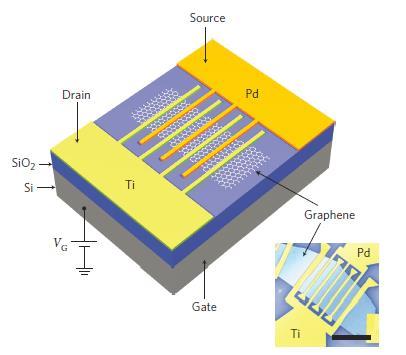
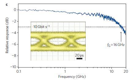
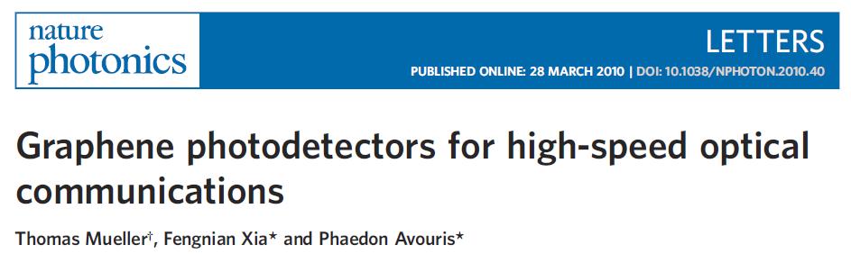
21 Photodiode based on graphene
22 Very high speed p-i-n photodiodes In optical communications systems operating at bit rates 10 Gbit/s or more, the photodiodes need to have very high bandwidths as well. Bandwidths of up to 70 GHz were demonstrated as early as 1986 using a very thin absorption layer (< 1 µm) and reducing the capacitance with a small size. This approach works but with the expense of lower responsivity and quantum efficiency. Since early 1990s several new approaches have been investigated for high-speed detectors. One example is illustrated in a figure below. The approach uses a channel waveguide-type configuration. Since the absorption takes place along the length of the waveguide (~ 10 µm), the quantum efficiency can be nearly 100%. From bandwidth point of view, the device can be optimized having an ultra-thin absorption layer resulting in very short collection time. a) Schematic cross section of a waveguide-photodiode and b) its measured frequency response:
23 Double heterostructure photodiodes As with semiconductor laser diodes, the performance of a p-i-n photodiode can be significantly improved by using a double-heterostructure design (sketched in figure below). The i-region is made of ternary compound In 0.53 Ga 0.47 As (lattice matched to InP) and is sandwiched between n- and p-type InP epitaxial layers. InP has a bandgap of ~ 1.35 ev, so it is transparent at wavelengths above ~ 0.92 µm. The middle InGaAs layer has a bandgap of ~ 0.75 ev, so it absorbs strongly within a wavelength range of about µm. Key features: The diffusive current component completely eliminated, since all the absorption occurs within the i-region. Quantum efficiency nearly 100% with 4-5 µm thick InGaAs layer. Sketch of an InGaAs photodiode based on double-heterostructure design: E g ( InP) E ( InGaAs) g

24 Schottky-Barrier Photodiodes Instead of a p layer, a thin semitransparent metallic film is used. Below shows (a) the structure and (b) energy band diagram of a Schottky barrier photodiodes. Minimum photon energy is W c, difference between the work function and the electron affinity. Examples of metal are Au on n-type Si and PtSi on p type silicon. Advantages 1) Not all semiconductors can be made in n and p type form. 2) MS junction has depletion layer at surface, with low surface recombination. 3) Majority carrier device with fast response and bandwidth ~ 100GHz. Low R and low RC because of metal.
25 Avalanche Photodiode Avalanche photodiodes (APDs) are preferred when the amount of optical power that can be spared for the receiver is limited. Their responsivity can significantly exceed 1 due to built in gain. The physical phenomenon behind the gain is known as impact ionization. Under certain conditions an accelerating electron can acquire sufficient energy to generate a new electron-hole pair. The net result is that a single primary electron creates many secondary electrons and holes, all of which contribute to the current. The generation rate is governed by two parameters, α e and α h, the impact-ionization coefficients for electrons and holes, respectively. Their numerical values depend on the semiconductor material and on the electric field that accelerates electrons and holes. Figure below shows the coefficients for several semiconductors. The values for α e and α h ~ 1x10⁻⁴ cm -1 are obtained for electric fields in the range of 2 4 x 10 5 V/m. Such high fields are obtained by applying a high voltage of ( ~ 100 V) to the APD. These values decreases with increasing temperature.
26 Avalanche Photodiodes Impact ionization processes resulting avalanche multiplication Electrode SiO 2 I photo R E h + e h > E g n+ p e h+ p+ E Electrode n + p Avalanche region e - E c x h + E v E(x) Impact of an energetic electron's kinetic energy excites VB electron to the CV. Absorption region Avalanche region x

27 Avalanche Photodiodes 1/ ae average distances between consecutive ionizations of electron 1/ a h average distances between consecutive ionizations of hole An important parameter for APD is the ionization ratio, k = a h /a e. For k << 1, most ionization is cause by electrons and avalanching occurs from left to right. For k ~ 1, we have holes to left generating electrons to right, creating a circulating path. This is not good because (1) of long time for carrier to stabilize, (2) of increase random and noise and (3) of increase chance of instability and breakdown. Ideal case is k=0 or k=infinity, where there is only one type of carrier to impact ionize. Multiplication factor M: M R APD I I APD ph MR 0 Responsivity R APD (A/W) for common APDs: Si: Ge: 3 30 InGaAs: 5 20

28 Response time Response time of APD is determined by the usual transit, diffusion and RC effects. In addition, APD has an avalanche buildup time, t m. w w d d t t m ve vh t m is in general a random statistical variable. For large gain G and for electron injection with 0 < k < 1, t m w v m ~ Gk e w v m h
29 Response time Avalanche buildup time in a silicon APD APD parameters w w v v e h d m 50 m 0.5 m G 100 k 0.1 cm / s 6 cm / s Antireflection coating Guard ring Avalanche breakdown n n + p p + Substrate Electrode Electrode SiO 2 n t wd wd wm wm Gk 1065 ps v v v v e h e h
30 Photodetector Noise Shot noise: Shot noise is related to the statistical fluctuation in both the photocurrent and the dark current. The magnitude of the shot noise is expressed as the root mean square (rms) noise current: q is charge of electron, 1.6*10-19 C Thermal or Johnson noise: The shunt resistance in a photodetector has a Johnson noise associated with it. This is due to the thermal generation of carriers. The magnitude of this generated current noise is: k B is Boltzmann Constant k B = 1.38 *10-23 J/K f is the operating bandwidth
31 Photodetector Noise Total Noise The total noise current generated in a photodetector is determined by: Noise Equivalent Power (NEP) Noise Equivalent Power is the amount of incident light power on a photodetector, which generates a photocurrent equal to the noise current. NEP is defined as:


32 APD example


33 Electrical wiring Reverse biased photodetector
34 Electrical wiring Amplified photodetector
35 Questions for thoughts Can we detect a single photon? Can you come up with a new kind of detector that is faster, more sensitive, and have less noise?
LEC E T C U T R U E R E 17 -Photodetectors
 LECTURE 17 -Photodetectors Topics to be covered Photodetectors PIN photodiode Avalanche Photodiode Photodetectors Principle of the p-n junction Photodiode A generic photodiode. Photodetectors Principle
Lecture 12. Semiconductor Detectors - Photodetectors
 Lecture 12 Semiconductor Detectors - Photodetectors Principle of the pn junction photodiode Absorption coefficient and photodiode materials Properties of semiconductor detectors The pin photodiodes Avalanche
Chapter 4. Photodetectors
 Chapter 4 Photodetectors Types of photodetectors: Photoconductos Photovoltaic Photodiodes Avalanche photodiodes (APDs) Resonant-cavity photodiodes MSM detectors In telecom we mainly use PINs and APDs.
Photosynthesis & Solar Power Harvesting
 Lecture 23 Semiconductor Detectors - Photodetectors Principle of the pn junction photodiode Absorption coefficient and photodiode materials Properties of semiconductor detectors The pin photodiodes Avalanche
Lect. 10: Photodetectors
 Photodetection: Absorption => Current Generation h Currents Materials for photodetection: E g < h Various methods for generating currents with photo-generated carriers: photoconductors, photodiodes, avalanche
Photodetector. Prof. Woo-Young Choi. Silicon Photonics (2012/2) Photodetection: Absorption => Current Generation. Currents
 Photodetection: Absorption => Current Generation. Currents") Photodetection: Absorption => Current Generation h Currents Materials for photodetection: E g < h Various methods for generating currents with photo-generated carriers: photoconductors, photodiodes, avalanche
Photodetection: Absorption => Current Generation h Currents Materials for photodetection: E g < h Various methods for generating currents with photo-generated carriers: photoconductors, photodiodes, avalanche
Photodetectors Read: Kasip, Chapter 5 Yariv, Chapter 11 Class Handout. ECE 162C Lecture #13 Prof. John Bowers
 Photodetectors Read: Kasip, Chapter 5 Yariv, Chapter 11 Class Handout ECE 162C Lecture #13 Prof. John Bowers Definitions Quantum efficiency η: Ratio of the number of electrons collected to the number of
Photodetector Basics
 Photodetection: Absorption => Current Generation hυ Currents Materials for photodetection: t ti E g
Single Photon detectors
 Single Photon detectors Outline Motivation for single photon detection Semiconductor; general knowledge and important background Photon detectors: internal and external photoeffect Properties of semiconductor
1 Name: Student number: DEPARTMENT OF PHYSICS AND PHYSICAL OCEANOGRAPHY MEMORIAL UNIVERSITY OF NEWFOUNDLAND. Fall :00-11:00
 1 Name: DEPARTMENT OF PHYSICS AND PHYSICAL OCEANOGRAPHY MEMORIAL UNIVERSITY OF NEWFOUNDLAND Final Exam Physics 3000 December 11, 2012 Fall 2012 9:00-11:00 INSTRUCTIONS: 1. Answer all seven (7) questions.
EE 5344 Introduction to MEMS CHAPTER 5 Radiation Sensors
 EE 5344 Introduction to MEMS CHAPTER 5 Radiation Sensors 5. Radiation Microsensors Radiation µ-sensors convert incident radiant signals into standard electrical out put signals. Radiant Signals Classification
Photonic Communications Engineering Lecture. Dr. Demetris Geddis Department of Engineering Norfolk State University
 Photonic Communications Engineering Lecture Dr. Demetris Geddis Department of Engineering Norfolk State University Light Detectors How does this detector work? Image from visionweb.com Responds to range
ECEN 5645 Introduc0on to Optoelectronics Class Mee0ng 25. Non- PIN Solid State Detectors
 ECEN 5645 Introduc0on to Optoelectronics Class Mee0ng 25 Non- PIN Solid State Detectors Today s Topics Avalanche Photodiodes Problem 5.6 APD Numerics and Examples Heterojunc0on Detectors Problem 5.10 Quantum
Photodiodes and other semiconductor devices
 Photodiodes and other semiconductor devices Chem 243 Winter 2017 What is a semiconductor? no e - Empty e levels Conduction Band a few e - Empty e levels Filled e levels Filled e levels lots of e - Empty
Electrons are shared in covalent bonds between atoms of Si. A bound electron has the lowest energy state.
 Photovoltaics Basic Steps the generation of light-generated carriers; the collection of the light-generated carriers to generate a current; the generation of a large voltage across the solar cell; and
EE 6313 Homework Assignments
 EE 6313 Homework Assignments 1. Homework I: Chapter 1: 1.2, 1.5, 1.7, 1.10, 1.12 [Lattice constant only] (Due Sept. 1, 2009). 2. Homework II: Chapter 1, 2: 1.17, 2.1 (a, c) (k = π/a at zone edge), 2.3
Purpose: To convert the received optical signal into an electrical lsignal.
 OPTICAL DETECTORS Optical Detectors Purpose: To convert the received optical signal into an electrical lsignal. Requirements For Detector HIGH SENSITIVITY (at operating wave lengths) at normal op. temp
Electron Energy, E E = 0. Free electron. 3s Band 2p Band Overlapping energy bands. 3p 3s 2p 2s. 2s Band. Electrons. 1s ATOM SOLID.
 Electron Energy, E Free electron Vacuum level 3p 3s 2p 2s 2s Band 3s Band 2p Band Overlapping energy bands Electrons E = 0 1s ATOM 1s SOLID In a metal the various energy bands overlap to give a single
Chemistry Instrumental Analysis Lecture 8. Chem 4631
 Chemistry 4631 Instrumental Analysis Lecture 8 UV to IR Components of Optical Basic components of spectroscopic instruments: stable source of radiant energy transparent container to hold sample device
Auxiliaire d enseignement Nicolas Ayotte
 2012-02-15 GEL 4203 / GEL 7041 OPTOÉLECTRONIQUE Auxiliaire d enseignement Nicolas Ayotte GEL 4203 / GEL 7041 Optoélectronique VI PN JUNCTION The density of charge sign Fixed charge density remaining 2
FYS3410 Condensed matter physics
 FYS3410 Condensed matter physics Lecture 23 and 24: pn-junctions and electrooptics Randi Haakenaasen UniK/UiO Forsvarets forskningsinstitutt 11.05.2016 and 18.05.2016 Outline Why pn-junctions are important
Solar cells operation
 Solar cells operation photovoltaic effect light and dark V characteristics effect of intensity effect of temperature efficiency efficency losses reflection recombination carrier collection and quantum
Lecture 5 Junction characterisation
 Lecture 5 Junction characterisation Jon Major October 2018 The PV research cycle Make cells Measure cells Despair Repeat 40 1.1% 4.9% Data Current density (ma/cm 2 ) 20 0-20 -1.0-0.5 0.0 0.5 1.0 Voltage
Comparison of Ge, InGaAs p-n junction solar cell
 ournal of Physics: Conference Series PAPER OPEN ACCESS Comparison of Ge, InGaAs p-n junction solar cell To cite this article: M. Korun and T. S. Navruz 16. Phys.: Conf. Ser. 77 135 View the article online
Thermionic Current Modeling and Equivalent Circuit of a III-V MQW P-I-N Photovoltaic Heterostructure
 Thermionic Current Modeling and Equivalent Circuit of a III-V MQW P-I-N Photovoltaic Heterostructure ARGYRIOS C. VARONIDES Physics and Electrical Engineering Department University of Scranton 800 Linden
OPTI510R: Photonics. Khanh Kieu College of Optical Sciences, University of Arizona Meinel building R.626
 OPTI510R: Photonics Khanh Kieu College of Optical Sciences, University of Arizona kkieu@optics.arizona.edu Meinel building R.626 Announcements HW#3 is assigned due Feb. 20 st Mid-term exam Feb 27, 2PM
n N D n p = n i p N A
 Summary of electron and hole concentration in semiconductors Intrinsic semiconductor: E G n kt i = pi = N e 2 0 Donor-doped semiconductor: n N D where N D is the concentration of donor impurity Acceptor-doped
Energetic particles and their detection in situ (particle detectors) Part II. George Gloeckler
 Part II. George Gloeckler") Energetic particles and their detection in situ (particle detectors) Part II George Gloeckler University of Michigan, Ann Arbor, MI University of Maryland, College Park, MD Simple particle detectors Gas-filled
Energetic particles and their detection in situ (particle detectors) Part II George Gloeckler University of Michigan, Ann Arbor, MI University of Maryland, College Park, MD Simple particle detectors Gas-filled
COURSE OUTLINE. Introduction Signals and Noise Filtering Sensors: PD5 Avalanche PhotoDiodes. Sensors, Signals and Noise 1
 Sensors, Signals and Noise 1 COURSE OUTLINE Introduction Signals and Noise Filtering Sensors: PD5 Avalanche PhotoDiodes Avalanche Photo-Diodes (APD) 2 Impact ionization in semiconductors Linear amplification
Current mechanisms Exam January 27, 2012
 Current mechanisms Exam January 27, 2012 There are four mechanisms that typically cause currents to flow: thermionic emission, diffusion, drift, and tunneling. Explain briefly which kind of current mechanisms
PN Junctions. Lecture 7
 Lecture 7 PN Junctions Kathy Aidala Applied Physics, G2 Harvard University 10 October, 2002 Wei 1 Active Circuit Elements Why are they desirable? Much greater flexibility in circuit applications. What
Spring Semester 2012 Final Exam
 Spring Semester 2012 Final Exam Note: Show your work, underline results, and always show units. Official exam time: 2.0 hours; an extension of at least 1.0 hour will be granted to anyone. Materials parameters
ECE 340 Lecture 27 : Junction Capacitance Class Outline:
 ECE 340 Lecture 27 : Junction Capacitance Class Outline: Breakdown Review Junction Capacitance Things you should know when you leave M.J. Gilbert ECE 340 Lecture 27 10/24/11 Key Questions What types of
PHOTODETECTORS AND SILICON PHOTO MULTIPLIER
 ESE seminar Photodetectors - Sipm, P. Jarron - F. Powolny 1 PHOTODETECTORS AND SILICON PHOTO MULTIPLIER ESE seminar Pierre Jarron, Francois Powolny OUTLINE 2 Brief history and overview of photodetectors
PHOTOVOLTAICS Fundamentals
 PHOTOVOLTAICS Fundamentals PV FUNDAMENTALS Semiconductor basics pn junction Solar cell operation Design of silicon solar cell SEMICONDUCTOR BASICS Allowed energy bands Valence and conduction band Fermi
Schottky Rectifiers Zheng Yang (ERF 3017,
 ECE442 Power Semiconductor Devices and Integrated Circuits Schottky Rectifiers Zheng Yang (ERF 3017, email: yangzhen@uic.edu) Power Schottky Rectifier Structure 2 Metal-Semiconductor Contact The work function
An Overview of the analysis of two dimensional back illuminated GaAs MESFET
 An Overview of the analysis of two dimensional back illuminated GaAs MESFET Prof. Lochan Jolly*, Ms. Sonia Thalavoor** *(A.P- Department of Electronics & Telecommunication, TCET, Mumbai Email: lochan.jolly@thakureducation.org)
8 Photo detectors. 8.1 Detector characteristics Responsivity R
 A photo detector is a device that converts the incident optical energy in a measurable signal, e.g., a voltage signal or an electric current. Photo detectors can be subdivided into two main classes: Photon
5. Semiconductors and P-N junction
 5. Semiconductors and P-N junction Thomas Zimmer, University of Bordeaux, France Summary Learning Outcomes... 2 Physical background of semiconductors... 2 The silicon crystal... 2 The energy bands... 3
Chapter 7. Solar Cell
 Chapter 7 Solar Cell 7.0 Introduction Solar cells are useful for both space and terrestrial application. Solar cells furnish the long duration power supply for satellites. It converts sunlight directly
Consider a uniformly doped PN junction, in which one region of the semiconductor is uniformly doped with acceptor atoms and the adjacent region is
 CHAPTER 7 The PN Junction Consider a uniformly doped PN junction, in which one region of the semiconductor is uniformly doped with acceptor atoms and the adjacent region is uniformly doped with donor atoms.
Chapter 7. The pn Junction
 Chapter 7 The pn Junction Chapter 7 PN Junction PN junction can be fabricated by implanting or diffusing donors into a P-type substrate such that a layer of semiconductor is converted into N type. Converting
MTLE-6120: Advanced Electronic Properties of Materials. Semiconductor p-n junction diodes. Reading: Kasap ,
 MTLE-6120: Advanced Electronic Properties of Materials 1 Semiconductor p-n junction diodes Reading: Kasap 6.1-6.5, 6.9-6.12 Metal-semiconductor contact potential 2 p-type n-type p-type n-type Same semiconductor
3.1 Absorption and Transparency
 3.1 Absorption and Transparency 3.1.1 Optical Devices (definitions) 3.1.2 Photon and Semiconductor Interactions 3.1.3 Photon Intensity 3.1.4 Absorption 3.1 Absorption and Transparency Objective 1: Recall
The photovoltaic effect occurs in semiconductors where there are distinct valence and
 How a Photovoltaic Cell Works The photovoltaic effect occurs in semiconductors where there are distinct valence and conduction bands. (There are energies at which electrons can not exist within the solid)
Carriers Concentration and Current in Semiconductors
 Carriers Concentration and Current in Semiconductors Carrier Transport Two driving forces for carrier transport: electric field and spatial variation of the carrier concentration. Both driving forces lead
Chapter 5. Semiconductor Laser
 Chapter 5 Semiconductor Laser 5.0 Introduction Laser is an acronym for light amplification by stimulated emission of radiation. Albert Einstein in 1917 showed that the process of stimulated emission must
Lecture 2. Introduction to semiconductors Structures and characteristics in semiconductors
 Lecture 2 Introduction to semiconductors Structures and characteristics in semiconductors Semiconductor p-n junction Metal Oxide Silicon structure Semiconductor contact Literature Glen F. Knoll, Radiation
Misan University College of Engineering Electrical Engineering Department. Exam: Final semester Date: 17/6/2017
 Misan University College of Engineering Electrical Engineering Department Subject: Electronic I Class: 1 st stage Exam: Final semester Date: 17/6/2017 Examiner: Dr. Baqer. O. TH. Time: 3 hr. Note: Answer
Peak Electric Field. Junction breakdown occurs when the peak electric field in the PN junction reaches a critical value. For the N + P junction,
 Peak Electric Field Junction breakdown occurs when the peak electric field in the P junction reaches a critical value. For the + P junction, qa E ( x) ( xp x), s W dep 2 s ( bi Vr ) 2 s potential barrier
Semiconductor Physics fall 2012 problems
 Semiconductor Physics fall 2012 problems 1. An n-type sample of silicon has a uniform density N D = 10 16 atoms cm -3 of arsenic, and a p-type silicon sample has N A = 10 15 atoms cm -3 of boron. For each
For the following statements, mark ( ) for true statement and (X) for wrong statement and correct it.
 for true statement and (X) for wrong statement and correct it.") Benha University Faculty of Engineering Shoubra Electrical Engineering Department First Year communications. Answer all the following questions Illustrate your answers with sketches when necessary. The
Benha University Faculty of Engineering Shoubra Electrical Engineering Department First Year communications. Answer all the following questions Illustrate your answers with sketches when necessary. The
Supplementary material for High responsivity mid-infrared graphene detectors with antenna-enhanced photo-carrier generation and collection
 Supplementary material for High responsivity mid-infrared graphene detectors with antenna-enhanced photo-carrier generation and collection Yu Yao 1, Raji Shankar 1, Patrick Rauter 1, Yi Song 2, Jing Kong
R. Ludwig and G. Bogdanov RF Circuit Design: Theory and Applications 2 nd edition. Figures for Chapter 6
 R. Ludwig and G. Bogdanov RF Circuit Design: Theory and Applications 2 nd edition Figures for Chapter 6 Free electron Conduction band Hole W g W C Forbidden Band or Bandgap W V Electron energy Hole Valence
February 1, 2011 The University of Toledo, Department of Physics and Astronomy SSARE, PVIC
 FUNDAMENTAL PROPERTIES OF SOLAR CELLS February 1, 2011 The University of Toledo, Department of Physics and Astronomy SSARE, PVIC Principles and Varieties of Solar Energy (PHYS 4400) and Fundamentals of
Appendix 1: List of symbols
 Appendix 1: List of symbols Symbol Description MKS Units a Acceleration m/s 2 a 0 Bohr radius m A Area m 2 A* Richardson constant m/s A C Collector area m 2 A E Emitter area m 2 b Bimolecular recombination
Fundamentals of Photovoltaics: C1 Problems. R.Treharne, K. Durose, J. Major, T. Veal, V.
 Fundamentals of Photovoltaics: C1 Problems R.Treharne, K. Durose, J. Major, T. Veal, V. Dhanak @cdtpv November 3, 2015 These problems will be highly relevant to the exam that you will sit very shortly.
PHYSICAL ELECTRONICS(ECE3540) CHAPTER 9 METAL SEMICONDUCTOR AND SEMICONDUCTOR HETERO-JUNCTIONS
 CHAPTER 9 METAL SEMICONDUCTOR AND SEMICONDUCTOR HETERO-JUNCTIONS") PHYSICAL ELECTRONICS(ECE3540) CHAPTER 9 METAL SEMICONDUCTOR AND SEMICONDUCTOR HETERO-JUNCTIONS Tennessee Technological University Wednesday, October 30, 013 1 Introduction Chapter 4: we considered the
PHYSICAL ELECTRONICS(ECE3540) CHAPTER 9 METAL SEMICONDUCTOR AND SEMICONDUCTOR HETERO-JUNCTIONS Tennessee Technological University Wednesday, October 30, 013 1 Introduction Chapter 4: we considered the
Classification of Solids
 Classification of Solids Classification by conductivity, which is related to the band structure: (Filled bands are shown dark; D(E) = Density of states) Class Electron Density Density of States D(E) Examples
Engineering 2000 Chapter 8 Semiconductors. ENG2000: R.I. Hornsey Semi: 1
 Engineering 2000 Chapter 8 Semiconductors ENG2000: R.I. Hornsey Semi: 1 Overview We need to know the electrical properties of Si To do this, we must also draw on some of the physical properties and we
EE 446/646 Photovoltaic Devices I. Y. Baghzouz
 EE 446/646 Photovoltaic Devices I Y. Baghzouz What is Photovoltaics? First used in about 1890, the word has two parts: photo, derived from the Greek word for light, volt, relating to electricity pioneer
Effective masses in semiconductors
 Effective masses in semiconductors The effective mass is defined as: In a solid, the electron (hole) effective mass represents how electrons move in an applied field. The effective mass reflects the inverse
Semiconductor Detectors
 Semiconductor Detectors Summary of Last Lecture Band structure in Solids: Conduction band Conduction band thermal conductivity: E g > 5 ev Valence band Insulator Charge carrier in conductor: e - Charge
3.1 Introduction to Semiconductors. Y. Baghzouz ECE Department UNLV
 3.1 Introduction to Semiconductors Y. Baghzouz ECE Department UNLV Introduction In this lecture, we will cover the basic aspects of semiconductor materials, and the physical mechanisms which are at the
Lecture 2. Introduction to semiconductors Structures and characteristics in semiconductors. Fabrication of semiconductor sensor
 Lecture 2 Introduction to semiconductors Structures and characteristics in semiconductors Semiconductor p-n junction Metal Oxide Silicon structure Semiconductor contact Fabrication of semiconductor sensor
Performance Analysis of an InGaAs Based p-i-n Photodetector
 Performance Analysis of an InGaAs Based p-i-n Photodetector Diponkar Kundu 1, Dilip Kumar Sarker 2, Md. Galib Hasan 3, Pallab Kanti Podder 4, Md. Masudur Rahman 5 Abstract an InGaAs based p-i-n photodetector
Session 6: Solid State Physics. Diode
 Session 6: Solid State Physics Diode 1 Outline A B C D E F G H I J 2 Definitions / Assumptions Homojunction: the junction is between two regions of the same material Heterojunction: the junction is between
UNIT - IV SEMICONDUCTORS AND MAGNETIC MATERIALS
 1. What is intrinsic If a semiconductor is sufficiently pure, then it is known as intrinsic semiconductor. ex:: pure Ge, pure Si 2. Mention the expression for intrinsic carrier concentration of intrinsic
Sensor Technology. Summer School: Advanced Microsystems Technologies for Sensor Applications
 Sensor Technology Summer School: Universidade Federal do Rio Grande do Sul (UFRGS) Porto Alegre, Brazil July 12 th 31 st, 2009 1 Outline of the Lecture: Philosophy of Sensing Instrumentation and Systems
p-n junction biasing, p-n I-V characteristics, p-n currents Norlaili Mohd. Noh EEE /09
 CLASS 6&7 p-n junction biasing, p-n I-V characteristics, p-n currents 1 p-n junction biasing Unbiased p-n junction: the potential barrier is 0.7 V for Si and 0.3 V for Ge. Nett current across the p-n junction
FYS 3028/8028 Solar Energy and Energy Storage. Calculator with empty memory Language dictionaries
 Faculty of Science and Technology Exam in: FYS 3028/8028 Solar Energy and Energy Storage Date: 11.05.2016 Time: 9-13 Place: Åsgårdvegen 9 Approved aids: Type of sheets (sqares/lines): Number of pages incl.
PHYSICAL ELECTRONICS(ECE3540) CHAPTER 9 METAL SEMICONDUCTOR AND SEMICONDUCTOR HETERO-JUNCTIONS
 CHAPTER 9 METAL SEMICONDUCTOR AND SEMICONDUCTOR HETERO-JUNCTIONS") PHYSICAL ELECTRONICS(ECE3540) CHAPTER 9 METAL SEMICONDUCTOR AND SEMICONDUCTOR HETERO-JUNCTIONS Tennessee Technological University Monday, November 11, 013 1 Introduction Chapter 4: we considered the semiconductor
PHYSICAL ELECTRONICS(ECE3540) CHAPTER 9 METAL SEMICONDUCTOR AND SEMICONDUCTOR HETERO-JUNCTIONS Tennessee Technological University Monday, November 11, 013 1 Introduction Chapter 4: we considered the semiconductor
Semiconductor Optoelectronics Prof. M. R. Shenoy Department of Physics Indian Institute of Technology, Delhi
 Semiconductor Optoelectronics Prof. M. R. Shenoy Department of Physics Indian Institute of Technology, Delhi Lecture - 1 Context and Scope of the Course (Refer Slide Time: 00:44) Welcome to this course
Sample Exam # 2 ECEN 3320 Fall 2013 Semiconductor Devices October 28, 2013 Due November 4, 2013
 Sample Exam # 2 ECEN 3320 Fall 203 Semiconductor Devices October 28, 203 Due November 4, 203. Below is the capacitance-voltage curve measured from a Schottky contact made on GaAs at T 300 K. Figure : Capacitance
collisions of electrons. In semiconductor, in certain temperature ranges the conductivity increases rapidly by increasing temperature
 1.9. Temperature Dependence of Semiconductor Conductivity Such dependence is one most important in semiconductor. In metals, Conductivity decreases by increasing temperature due to greater frequency of
Unit IV Semiconductors Engineering Physics
 Introduction A semiconductor is a material that has a resistivity lies between that of a conductor and an insulator. The conductivity of a semiconductor material can be varied under an external electrical
Lab #5 Current/Voltage Curves, Efficiency Measurements and Quantum Efficiency
 Lab #5 Current/Voltage Curves, Efficiency Measurements and Quantum Efficiency R.J. Ellingson and M.J. Heben November 4, 2014 PHYS 4580, 6280, and 7280 Simple solar cell structure The Diode Equation Ideal
Semiconductor Physical Electronics
 Semiconductor Physical Electronics Sheng S. Li Department of Electrical Engineering University of Florida Gainesville, Florida Plenum Press New York and London Contents CHAPTER 1. Classification of Solids
Lecture 15: Optoelectronic devices: Introduction
 Lecture 15: Optoelectronic devices: Introduction Contents 1 Optical absorption 1 1.1 Absorption coefficient....................... 2 2 Optical recombination 5 3 Recombination and carrier lifetime 6 3.1
UNIVERSITY OF CALIFORNIA College of Engineering Department of Electrical Engineering and Computer Sciences. EECS 130 Professor Ali Javey Fall 2006
 UNIVERSITY OF CALIFORNIA College of Engineering Department of Electrical Engineering and Computer Sciences EECS 130 Professor Ali Javey Fall 2006 Midterm 2 Name: SID: Closed book. Two sheets of notes are
EE 5611 Introduction to Microelectronic Technologies Fall Tuesday, September 23, 2014 Lecture 07
 EE 5611 Introduction to Microelectronic Technologies Fall 2014 Tuesday, September 23, 2014 Lecture 07 1 Introduction to Solar Cells Topics to be covered: Solar cells and sun light Review on semiconductor
Fundamentals of Semiconductor Physics
 Fall 2007 Fundamentals of Semiconductor Physics 万 歆 Zhejiang Institute of Modern Physics xinwan@zimp.zju.edu.cn http://zimp.zju.edu.cn/~xinwan/ Transistor technology evokes new physics The objective of
Lecture 8. Equations of State, Equilibrium and Einstein Relationships and Generation/Recombination
 Lecture 8 Equations of State, Equilibrium and Einstein Relationships and Generation/Recombination Reading: (Cont d) Notes and Anderson 2 sections 3.4-3.11 Energy Equilibrium Concept Consider a non-uniformly
Schottky Diodes (M-S Contacts)
") Schottky Diodes (M-S Contacts) Three MITs of the Day Band diagrams for ohmic and rectifying Schottky contacts Similarity to and difference from bipolar junctions on electrostatic and IV characteristics.
Schottky Diodes (M-S Contacts) Three MITs of the Day Band diagrams for ohmic and rectifying Schottky contacts Similarity to and difference from bipolar junctions on electrostatic and IV characteristics.
OPTI510R: Photonics. Khanh Kieu College of Optical Sciences, University of Arizona Meinel building R.626
 OPTI510R: Photonics Khanh Kieu College of Optical Sciences, University of Arizona kkieu@optics.arizona.edu Meinel building R.626 Announcements HW #6 is assigned, due April 23 rd Final exam May 2 Semiconductor
Course overview. Me: Dr Luke Wilson. The course: Physics and applications of semiconductors. Office: E17 open door policy
 Course overview Me: Dr Luke Wilson Office: E17 open door policy email: luke.wilson@sheffield.ac.uk The course: Physics and applications of semiconductors 10 lectures aim is to allow time for at least one
Electronics The basics of semiconductor physics
 Electronics The basics of semiconductor physics Prof. Márta Rencz, Gergely Nagy BME DED September 16, 2013 The basic properties of semiconductors Semiconductors conductance is between that of conductors
Lecture 2. Introduction to semiconductors Structures and characteristics in semiconductors
 Lecture 2 Introduction to semiconductors Structures and characteristics in semiconductors Semiconductor p-n junction Metal Oxide Silicon structure Semiconductor contact Literature Glen F. Knoll, Radiation
e - Galvanic Cell 1. Voltage Sources 1.1 Polymer Electrolyte Membrane (PEM) Fuel Cell
 Fuel Cell") Galvanic cells convert different forms of energy (chemical fuel, sunlight, mechanical pressure, etc.) into electrical energy and heat. In this lecture, we are interested in some examples of galvanic cells.
Galvanic cells convert different forms of energy (chemical fuel, sunlight, mechanical pressure, etc.) into electrical energy and heat. In this lecture, we are interested in some examples of galvanic cells.
ECE-342 Test 2 Solutions, Nov 4, :00-8:00pm, Closed Book (one page of notes allowed)
") ECE-342 Test 2 Solutions, Nov 4, 2008 6:00-8:00pm, Closed Book (one page of notes allowed) Please use the following physical constants in your calculations: Boltzmann s Constant: Electron Charge: Free
ECE-342 Test 2 Solutions, Nov 4, 2008 6:00-8:00pm, Closed Book (one page of notes allowed) Please use the following physical constants in your calculations: Boltzmann s Constant: Electron Charge: Free
Solid State Electronics. Final Examination
 The University of Toledo EECS:4400/5400/7400 Solid State Electronic Section elssf08fs.fm - 1 Solid State Electronics Final Examination Problems Points 1. 1. 14 3. 14 Total 40 Was the exam fair? yes no
Supplementary Figure 1. Supplementary Figure 1 Characterization of another locally gated PN junction based on boron
 Supplementary Figure 1 Supplementary Figure 1 Characterization of another locally gated PN junction based on boron nitride and few-layer black phosphorus (device S1). (a) Optical micrograph of device S1.
Introduction to Semiconductor Physics. Prof.P. Ravindran, Department of Physics, Central University of Tamil Nadu, India
 Introduction to Semiconductor Physics 1 Prof.P. Ravindran, Department of Physics, Central University of Tamil Nadu, India http://folk.uio.no/ravi/cmp2013 Review of Semiconductor Physics Semiconductor fundamentals
Chapter 3 The InAs-Based nbn Photodetector and Dark Current
 68 Chapter 3 The InAs-Based nbn Photodetector and Dark Current The InAs-based nbn photodetector, which possesses a design that suppresses surface leakage current, is compared with both a commercially available
16EC401 BASIC ELECTRONIC DEVICES UNIT I PN JUNCTION DIODE. Energy Band Diagram of Conductor, Insulator and Semiconductor:
 16EC401 BASIC ELECTRONIC DEVICES UNIT I PN JUNCTION DIODE Energy bands in Intrinsic and Extrinsic silicon: Energy Band Diagram of Conductor, Insulator and Semiconductor: 1 2 Carrier transport: Any motion
PN Junction
 P Junction 2017-05-04 Definition Power Electronics = semiconductor switches are used Analogue amplifier = high power loss 250 200 u x 150 100 u Udc i 50 0 0 50 100 150 200 250 300 350 400 i,u dc i,u u
This is the 15th lecture of this course in which we begin a new topic, Excess Carriers. This topic will be covered in two lectures.
 Solid State Devices Dr. S. Karmalkar Department of Electronics and Communication Engineering Indian Institute of Technology, Madras Lecture - 15 Excess Carriers This is the 15th lecture of this course
Graphene photodetectors with ultra-broadband and high responsivity at room temperature
 SUPPLEMENTARY INFORMATION DOI: 10.1038/NNANO.2014.31 Graphene photodetectors with ultra-broadband and high responsivity at room temperature Chang-Hua Liu 1, You-Chia Chang 2, Ted Norris 1.2* and Zhaohui
EECS130 Integrated Circuit Devices
 EECS130 Integrated Circuit Devices Professor Ali Javey 9/18/2007 P Junctions Lecture 1 Reading: Chapter 5 Announcements For THIS WEEK OLY, Prof. Javey's office hours will be held on Tuesday, Sept 18 3:30-4:30
Semiconductor Physics fall 2012 problems
 Semiconductor Physics fall 2012 problems 1. An n-type sample of silicon has a uniform density N D = 10 16 atoms cm -3 of arsenic, and a p-type silicon sample has N A = 10 15 atoms cm -3 of boron. For each