Lab #5 Current/Voltage Curves, Efficiency Measurements and Quantum Efficiency
|
|
|
- Corey McKinney
- 5 years ago
- Views:
Transcription
1 Lab #5 Current/Voltage Curves, Efficiency Measurements and Quantum Efficiency R.J. Ellingson and M.J. Heben November 4, 2014 PHYS 4580, 6280, and 7280

2 Simple solar cell structure
. I 0 is a property of the junction interfaces and recombination in the device. http://en.wikipedia.")
3 The Diode Equation Ideal Diode Law I = net current; I 0 = "dark saturation current", aka diode leakage current, aka reverse saturation current; V = applied voltage across the terminals of the diode; q = electron charge; k = Boltzmann's constant; T = absolute temperature (K). I 0 is a property of the junction interfaces and recombination in the device.
4 Light Generated Current is Opposite Direction of Forward Dark Current hν + J Light - J Forward Principle of Superposition I qv I0 exp 1 nkt I L Where n is the diode quality factor, reflects type of recombination in the device
5 Homojunction solar cell (e.g., Silicon) p-type emitter (window) n-type base (absorber) n-type emitter (window) p-type base (absorber) + - Before contact - + V bi At equilibrium J L hν J L Typical Si device configuration +J +J under forward bias +J under forward bias J L +V + - J/V? - + J/V? J L Light Generated Current is Opposite Direction of Forward Dark Current
6 IV Curve The IV curve of a solar cell is the superposition of the IV curve in the dark with a constant light-generated current (I L ). The light current shift the J/V curve down so V OC occurs near the turn-on knee in the diode curve. I L = light generated current. I qv I0 exp 1 nkt I L Go to Animation Lindholm, F. A., J. G. Fossum, and E. L. Burgess, "Application of the superposition principle to solar-cell analysis", IEEE Transactions on Electron Devices, vol. 26, no. 3, pp , 1979.

7 Short circuit photocurrent The short-circuit current (I SC ) is the current through the solar cell when the voltage across the solar cell is zero (i.e., when the solar cell is short circuited). Usually written as I SC, the short-circuit current is shown on the IV curve below. I SC is due to the generation and collection of light-generated carriers. For an ideal PV cell with moderate resistive loss, I SC and the light-generated current are identical (I SC is the largest current which may be drawn from the solar cell).
8 Short circuit (photo)current (I SC ) or current density (J SC ) I SC (or J SC ) is the current (or current density) when the device leads are shorted (i.e., connected electrically to one another) I SC depends on a number of factors, as follows : the area of the solar cell. To remove the dependence of the solar cell area, it is more common to list the short-circuit current density (J sc in ma/cm 2 ) rather than the short-circuit current; the number of photons (i.e., the power of the incident light source). Isc from a solar cell is directly dependant on the light intensity; the spectrum of the incident light. For most solar cell measurement, the spectrum is standardised to the AM1.5 spectrum; the optical properties (absorption and reflection) of the solar cell (discussed in Optical Losses); and the collection probability of the solar cell, which depends chiefly on the surface passivation and the minority carrier lifetime in the absorber.
9 Open circuit photovoltage (V OC ) The open-circuit voltage, V oc, is the maximum voltage available from a solar cell, and this occurs at zero current. I qv I0 exp 1 nkt I L V OC nkt I L ln 1 q Io An equation for V oc is found by setting the total current (I) to zero in the expression for the ideal solar cell.
 is an important parameter for determining the maximum power from a solar cell. The FF is the ratio of the maximum power from the solar cell to the product of V oc and I sc.")
10 Solar cell fill factor (FF) and Max Power Point (mpp) At I SC and V OC, the power from the solar cell is zero. The "fill factor (FF) is an important parameter for determining the maximum power from a solar cell. The FF is the ratio of the maximum power from the solar cell to the product of V oc and I sc. Graphically, the FF is a measure of the area of the largest rectangle which will fit in the IV curve. P out = I * V dp/dv = 0
11 Solar cell efficiency The efficiency of a solar cell (sometimes known as the power conversion efficiency, or PCE, and also often abbreviated η) represents the ratio where the output electrical power at the maximum power point on the IV curve is divided by the incident light power typically using a standard AM1.5G simulated solar spectrum. The efficiency of a solar cell is determined as the fraction of incident power which is converted to electricity and is defined as: P max V OC I SC FF where V oc is the open-circuit voltage; where I sc is the short-circuit current; and where FF is the fill factor where η is the efficiency. V Power in AM1.5G spectrum is 1kW/m 2, or 100 mw/cm 2 For a 10 x 10 cm 2 cell, the input power (AM1.5G) is 100 mw/cm 2 x 100 cm 2 = 10 W. OC I P SC inc FF

 Diode equation with R")
12 Current density (ma/cm 2 ) Impact of Electrical Loss Due to High Series Resistance (R S ) PV cells R SH = 10,000 Volts (V) Diode equation with R S and R SH :
13
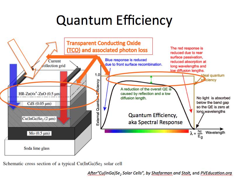
14 Quantum Efficiency (also known as the Spectral Response) Determined as a function of wavelength Is the ratio of incident # of photons to the numbers of electron-hole pairs that flow in the external circuit. There are two versions of QE; External QE (EQE) - considers all photons incident on the device. Internal QE (IQE) considers only photons that are absorbed in the active region of the device Clearly, it is much more straightforward to measure EQE than IQE The QE cannot never exceed 1 (or 100%) QE measurements are generally done at short circuit where the electric field within the device is large, but can also be done at any bias voltage and can reveal information about recombination in the PV device.
February 1, 2011 The University of Toledo, Department of Physics and Astronomy SSARE, PVIC
 FUNDAMENTAL PROPERTIES OF SOLAR CELLS February 1, 2011 The University of Toledo, Department of Physics and Astronomy SSARE, PVIC Principles and Varieties of Solar Energy (PHYS 4400) and Fundamentals of
EE 5611 Introduction to Microelectronic Technologies Fall Tuesday, September 23, 2014 Lecture 07
 EE 5611 Introduction to Microelectronic Technologies Fall 2014 Tuesday, September 23, 2014 Lecture 07 1 Introduction to Solar Cells Topics to be covered: Solar cells and sun light Review on semiconductor
PHOTOVOLTAICS Fundamentals
 PHOTOVOLTAICS Fundamentals PV FUNDAMENTALS Semiconductor basics pn junction Solar cell operation Design of silicon solar cell SEMICONDUCTOR BASICS Allowed energy bands Valence and conduction band Fermi
Fundamentals of Photovoltaics: C1 Problems. R.Treharne, K. Durose, J. Major, T. Veal, V.
 Fundamentals of Photovoltaics: C1 Problems R.Treharne, K. Durose, J. Major, T. Veal, V. Dhanak @cdtpv November 3, 2015 These problems will be highly relevant to the exam that you will sit very shortly.
Solar cells operation
 Solar cells operation photovoltaic effect light and dark V characteristics effect of intensity effect of temperature efficiency efficency losses reflection recombination carrier collection and quantum
Electronic Supplementary Information. Recombination kinetics in silicon solar cell under low-concentration: Electroanalytical
 Electronic Supplementary Material (ESI) for Physical Chemistry Chemical Physics. This journal is the Owner Societies 2014 Electronic Supplementary Information Recombination kinetics in silicon solar cell
Lecture 5 Junction characterisation
 Lecture 5 Junction characterisation Jon Major October 2018 The PV research cycle Make cells Measure cells Despair Repeat 40 1.1% 4.9% Data Current density (ma/cm 2 ) 20 0-20 -1.0-0.5 0.0 0.5 1.0 Voltage
ET3034TUx External parameters of an ideal solar cell. How can we determine the performance of a solar cell?
 ET3034TUx - 3.2.1 - External parameters of an ideal solar cell How can we determine the performance of a solar cell? In the previous block we have introduced the J- V curve of an ideal solar cell and its
Toward a 1D Device Model Part 1: Device Fundamentals
 Toward a 1D Device Model Part 1: Device Fundamentals Lecture 7 9/29/2011 MIT Fundamentals of Photovoltaics 2.626/2.627 Fall 2011 Prof. Tonio Buonassisi 1 Learning Objectives: Toward a 1D Device Model 1.
Electrons are shared in covalent bonds between atoms of Si. A bound electron has the lowest energy state.
 Photovoltaics Basic Steps the generation of light-generated carriers; the collection of the light-generated carriers to generate a current; the generation of a large voltage across the solar cell; and
Chapter 7. Solar Cell
 Chapter 7 Solar Cell 7.0 Introduction Solar cells are useful for both space and terrestrial application. Solar cells furnish the long duration power supply for satellites. It converts sunlight directly
Organic Electronic Devices
 Organic Electronic Devices Week 4: Organic Photovoltaic Devices Lecture 4.2: Characterizing Device Parameters in OPVs Bryan W. Boudouris Chemical Engineering Purdue University 1 Lecture Overview and Learning
Ideal Diode Equation II + Intro to Solar Cells
 ECE-35: Spring 15 Ideal Diode Equation II + Intro to Solar Cells Professor Mark Lundstrom Electrical and Computer Engineering Purdue University, West Lafayette, IN USA lundstro@purdue.edu Pierret, Semiconductor
Comparison of Ge, InGaAs p-n junction solar cell
 ournal of Physics: Conference Series PAPER OPEN ACCESS Comparison of Ge, InGaAs p-n junction solar cell To cite this article: M. Korun and T. S. Navruz 16. Phys.: Conf. Ser. 77 135 View the article online
ρ ρ LED access resistances d A W d s n s p p p W the output window size p-layer d p series access resistance d n n-layer series access resistance
 LED access resistances W the output window size p-layer series access resistance d p n-layer series access resistance d n The n-layer series access resistance R = ρ s n where the resistivity of the n-layer
Lab #6 Measuring the Spectral Response of a PV Cell
 Lab #6 Measuring the Spectral Response of a PV Cell R.J. Ellingson and M.J. Heben November 5, 2013 PHYS 4580, 6/7280 Pop Quiz Note: quiz does not count toward grade In which spectral region do most solar
Thermionic Current Modeling and Equivalent Circuit of a III-V MQW P-I-N Photovoltaic Heterostructure
 Thermionic Current Modeling and Equivalent Circuit of a III-V MQW P-I-N Photovoltaic Heterostructure ARGYRIOS C. VARONIDES Physics and Electrical Engineering Department University of Scranton 800 Linden
Analyze the effect of window layer (AlAs) for increasing the efficiency of GaAs based solar cell
 for increasing the efficiency of GaAs based solar cell") American Journal of Engineering Research (AJER) e-issn: 2320-0847 p-issn : 2320-0936 Volume-4, Issue-7, pp-304-315 www.ajer.org Research Paper Open Access Analyze the effect of window layer (AlAs) for
American Journal of Engineering Research (AJER) e-issn: 2320-0847 p-issn : 2320-0936 Volume-4, Issue-7, pp-304-315 www.ajer.org Research Paper Open Access Analyze the effect of window layer (AlAs) for
Explanation of Light/Dark Superposition Failure in CIGS Solar Cells
 Mat. Res. Soc. Symp. Proc. Vol. 763 23 Materials Research Society B5.2.1 Explanation of / Superposition Failure in CIGS Solar Cells Markus Gloeckler, Caroline R. Jenkins, and James R. Sites Physics Department,
Lecture 2. Photon in, Electron out: Basic Principle of PV
 Lecture 2 Photon in, Electron out: Basic Principle of PV References: 1. Physics of Solar Cells. Jenny Nelson. Imperial College Press, 2003. 2. Third Generation Photovoltaics: Advanced Solar Energy Conversion.
Photovoltaic cell and module physics and technology. Vitezslav Benda, Prof Czech Technical University in Prague
 Photovoltaic cell and module physics and technology Vitezslav Benda, Prof Czech Technical University in Prague benda@fel.cvut.cz www.fel.cvut.cz 1 Outlines Photovoltaic Effect Photovoltaic cell structure
Solar Photovoltaics & Energy Systems
 Solar Photovoltaics & Energy Systems Lecture 4. Crystalline Semiconductor Based Solar Cells ChE-600 Wolfgang Tress, May 2016 1 Photovoltaic Solar Energy Conversion 2 Semiconductor vs. Heat Engine spectral
Lab 2. Characterization of Solar Cells
 Lab 2. Characterization of Solar Cells Physics Enhancement Programme Department of Physics, Hong Kong Baptist University 1. OBJECTIVES To familiarize with the principles of commercial solar cells To characterize
Chapter 6 Solar Cells (Supplementary)
") 1 Chapter 6 olar Cells (upplementary) Chapter 6... 1 olar Cells... 1 6.1.1... 6.1.... 6.1.3... 6.1.4 Effect of Minority Electron Lifetime on Efficiency... 6.1.5 Effect of Minority hole Lifetime on Efficiency...
1 Chapter 6 olar Cells (upplementary) Chapter 6... 1 olar Cells... 1 6.1.1... 6.1.... 6.1.3... 6.1.4 Effect of Minority Electron Lifetime on Efficiency... 6.1.5 Effect of Minority hole Lifetime on Efficiency...
Semiconductor Junctions
 8 Semiconductor Junctions Almost all solar cells contain junctions between different materials of different doping. Since these junctions are crucial to the operation of the solar cell, we will discuss
3.003 Principles of Engineering Practice
 3.003 Principles of Engineering Practice One Month Review Solar Cells The Sun Semiconductors pn junctions Electricity 1 Engineering Practice 1. Problem Definition 2. Constraints 3. Options 4. Analysis
Solar Photovoltaics & Energy Systems
 Solar Photovoltaics & Energy Systems Lecture 3. Crystalline Semiconductor Based Solar Cells ChE-600 Wolfgang Tress, March 2018 1 Photovoltaic Solar Energy Conversion 2 Outline Recap: Thermodynamics of
n N D n p = n i p N A
 Summary of electron and hole concentration in semiconductors Intrinsic semiconductor: E G n kt i = pi = N e 2 0 Donor-doped semiconductor: n N D where N D is the concentration of donor impurity Acceptor-doped
Photovoltaic cell and module physics and technology
 Photovoltaic cell and module physics and technology Vitezslav Benda, Prof Czech Technical University in Prague benda@fel.cvut.cz www.fel.cvut.cz 6/21/2012 1 Outlines Photovoltaic Effect Photovoltaic cell
The Role of doping in the window layer on Performance of a InP Solar Cells USING AMPS-1D
 IOSR Journal of Engineering (IOSRJEN) ISSN: 2250-3021 Volume 2, Issue 8(August 2012), PP 42-46 The Role of doping in the window layer on Performance of a InP Solar Cells USING AMPS-1D Dennai Benmoussa
ET3034TUx Utilization of band gap energy
 ET3034TUx - 3.3.1 - Utilization of band gap energy In the last two weeks we have discussed the working principle of a solar cell and the external parameters that define the performance of a solar cell.
OPTI510R: Photonics. Khanh Kieu College of Optical Sciences, University of Arizona Meinel building R.626
 OPTI510R: Photonics Khanh Kieu College of Optical Sciences, University of Arizona kkieu@optics.arizona.edu Meinel building R.626 Announcements Homework #6 is assigned, due May 1 st Final exam May 8, 10:30-12:30pm
FYS 3028/8028 Solar Energy and Energy Storage. Calculator with empty memory Language dictionaries
 Faculty of Science and Technology Exam in: FYS 3028/8028 Solar Energy and Energy Storage Date: 11.05.2016 Time: 9-13 Place: Åsgårdvegen 9 Approved aids: Type of sheets (sqares/lines): Number of pages incl.
Lecture 35 - Bipolar Junction Transistor (cont.) November 27, Current-voltage characteristics of ideal BJT (cont.)
 November 27, Current-voltage characteristics of ideal BJT (cont.)") 6.720J/3.43J - Integrated Microelectronic Devices - Fall 2002 Lecture 35-1 Lecture 35 - Bipolar Junction Transistor (cont.) November 27, 2002 Contents: 1. Current-voltage characteristics of ideal BJT (cont.)
6.720J/3.43J - Integrated Microelectronic Devices - Fall 2002 Lecture 35-1 Lecture 35 - Bipolar Junction Transistor (cont.) November 27, 2002 Contents: 1. Current-voltage characteristics of ideal BJT (cont.)
Fundamental Limitations of Solar Cells
 2018 Lecture 2 Fundamental Limitations of Solar Cells Dr Kieran Cheetham MPhys (hons) CPhys MInstP MIET L3 Key Question Why can't a solar cell have a 100% efficiency? (Or even close to 100%?) Can you answer
MODELING THE FUNDAMENTAL LIMIT ON CONVERSION EFFICIENCY OF QD SOLAR CELLS
 MODELING THE FUNDAMENTAL LIMIT ON CONVERSION EFFICIENCY OF QD SOLAR CELLS Ա.Մ.Կեչիյանց Ara Kechiantz Institute of Radiophysics and Electronics (IRPhE), National Academy of Sciences (Yerevan, Armenia) Marseille
Supplementary Information
 Supplementary Information Supplementary Figures Supplementary Figure S1. Change in open circuit potential ( OCP) of 1% W-doped BiVO 4 photoanode upon illumination with different light intensities. Above
1 Name: Student number: DEPARTMENT OF PHYSICS AND PHYSICAL OCEANOGRAPHY MEMORIAL UNIVERSITY OF NEWFOUNDLAND. Fall :00-11:00
 1 Name: DEPARTMENT OF PHYSICS AND PHYSICAL OCEANOGRAPHY MEMORIAL UNIVERSITY OF NEWFOUNDLAND Final Exam Physics 3000 December 11, 2012 Fall 2012 9:00-11:00 INSTRUCTIONS: 1. Answer all seven (7) questions.
Paper Review. Special Topics in Optical Engineering II (15/1) Minkyu Kim. IEEE Journal of Quantum Electronics, Feb 1985
 Minkyu Kim. IEEE Journal of Quantum Electronics, Feb 1985") Paper Review IEEE Journal of Quantum Electronics, Feb 1985 Contents Semiconductor laser review High speed semiconductor laser Parasitic elements limitations Intermodulation products Intensity noise Large
Paper Review IEEE Journal of Quantum Electronics, Feb 1985 Contents Semiconductor laser review High speed semiconductor laser Parasitic elements limitations Intermodulation products Intensity noise Large
Photovoltaic Energy Conversion. Frank Zimmermann
 Photovoltaic Energy Conversion Frank Zimmermann Solar Electricity Generation Consumes no fuel No pollution No greenhouse gases No moving parts, little or no maintenance Sunlight is plentiful & inexhaustible
3.1 Absorption and Transparency
 3.1 Absorption and Transparency 3.1.1 Optical Devices (definitions) 3.1.2 Photon and Semiconductor Interactions 3.1.3 Photon Intensity 3.1.4 Absorption 3.1 Absorption and Transparency Objective 1: Recall
Photodiodes and other semiconductor devices
 Photodiodes and other semiconductor devices Chem 243 Winter 2017 What is a semiconductor? no e - Empty e levels Conduction Band a few e - Empty e levels Filled e levels Filled e levels lots of e - Empty
Chapter 3 Modeling and Simulation of Dye-Sensitized Solar Cell
 Chapter 3 Modeling and Simulation of Dye-Sensitized Solar Cell 3.1. Introduction In recent years, dye-sensitized solar cells (DSSCs) based on nanocrystalline mesoporous TiO 2 films have attracted much
Photon Extraction: the key physics for approaching solar cell efficiency limits
 Photon Extraction: the key physics for approaching solar cell efficiency limits Owen Miller*: Post-doc, MIT Math Eli Yablonovitch: UC Berkeley, LBNL Slides/Codes/Relevant Papers: math.mit.edu/~odmiller/publications
5. Semiconductors and P-N junction
 5. Semiconductors and P-N junction Thomas Zimmer, University of Bordeaux, France Summary Learning Outcomes... 2 Physical background of semiconductors... 2 The silicon crystal... 2 The energy bands... 3
Supplementary Figures
 Supplementary Figures Supplementary Figure 1. AFM profiles of the charge transport and perovskite layers. AFM Image showing the thickness (y axis) of the layer with respect to the horizontal position of
Supplementary Figure 1. Supplementary Figure 1 Characterization of another locally gated PN junction based on boron
 Supplementary Figure 1 Supplementary Figure 1 Characterization of another locally gated PN junction based on boron nitride and few-layer black phosphorus (device S1). (a) Optical micrograph of device S1.
Planar Organic Photovoltaic Device. Saiful I. Khondaker
 Planar Organic Photovoltaic Device Saiful I. Khondaker Nanoscience Technology Center and Department of Physics University of Central Florida http://www.physics.ucf.edu/~khondaker W Metal 1 L ch Metal 2
The Opto-Electronic Physics That Just Broke the Efficiency Record in Solar Cells
 The Opto-Electronic Physics That Just Broke the Efficiency Record in Solar Cells Solar Energy Mini-Series Jen-Hsun Huang Engineering Center Stanford, California Sept. 26, 2011 Owen D. Miller & Eli Yablonovitch
Organic Electronic Devices
 Organic Electronic Devices Week 4: Organic Photovoltaic Devices Lecture 4.1: Overview of Organic Photovoltaic Devices Bryan W. Boudouris Chemical Engineering Purdue University 1 Lecture Overview and Learning
Semiconductor Physics and Devices
 The pn Junction 1) Charge carriers crossing the junction. 3) Barrier potential Semiconductor Physics and Devices Chapter 8. The pn Junction Diode 2) Formation of positive and negative ions. 4) Formation
The temperature dependence of the spectral and e ciency behavior of Si solar cell under low concentrated solar radiation
 Renewable Energy 21 (2000) 445±458 www.elsevier.com/locate/renene The temperature dependence of the spectral and e ciency behavior of Si solar cell under low concentrated solar radiation M.A. Mosalam Shaltout
Lecture 17. The Bipolar Junction Transistor (II) Regimes of Operation. Outline
 Regimes of Operation. Outline") Lecture 17 The Bipolar Junction Transistor (II) Regimes of Operation Outline Regimes of operation Large-signal equivalent circuit model Output characteristics Reading Assignment: Howe and Sodini; Chapter
Lecture 17 The Bipolar Junction Transistor (II) Regimes of Operation Outline Regimes of operation Large-signal equivalent circuit model Output characteristics Reading Assignment: Howe and Sodini; Chapter
Thermally Stable Silver Nanowires-embedding. Metal Oxide for Schottky Junction Solar Cells
 Supporting Information Thermally Stable Silver Nanowires-embedding Metal Oxide for Schottky Junction Solar Cells Hong-Sik Kim, 1 Malkeshkumar Patel, 1 Hyeong-Ho Park, Abhijit Ray, Chaehwan Jeong, # and
Solar Cell Physics: recombination and generation
 NCN Summer School: July 2011 Solar Cell Physics: recombination and generation Prof. Mark Lundstrom lundstro@purdue.edu Electrical and Computer Engineering Purdue University West Lafayette, Indiana USA
Lecture 15 - The pn Junction Diode (I) I-V Characteristics. November 1, 2005
 I-V Characteristics. November 1, 2005") 6.012 - Microelectronic Devices and Circuits - Fall 2005 Lecture 15-1 Lecture 15 - The pn Junction Diode (I) I-V Characteristics November 1, 2005 Contents: 1. pn junction under bias 2. I-V characteristics
6.012 - Microelectronic Devices and Circuits - Fall 2005 Lecture 15-1 Lecture 15 - The pn Junction Diode (I) I-V Characteristics November 1, 2005 Contents: 1. pn junction under bias 2. I-V characteristics
Semiconductor Physics fall 2012 problems
 Semiconductor Physics fall 2012 problems 1. An n-type sample of silicon has a uniform density N D = 10 16 atoms cm -3 of arsenic, and a p-type silicon sample has N A = 10 15 atoms cm -3 of boron. For each
2.626 / 2.627: Fundamentals of Photovoltaics Problem Set #3 Prof. Tonio Buonassisi
 2.626 / 2.627: Fundamentals of Photovoltaics Problem Set #3 Prof. Tonio Buonassisi Please note: Excel spreadsheets or Matlab code may be used to calculate the answers to many of the problems below, but
Introduction. Katarzyna Skorupska. Silicon will be used as the model material however presented knowledge applies to other semiconducting materials
 Introduction Katarzyna Skorupska Silicon will be used as the model material however presented knowledge applies to other semiconducting materials 2 June 26 Intrinsic and Doped Semiconductors 3 July 3 Optical
Semiconductor Physics fall 2012 problems
 Semiconductor Physics fall 2012 problems 1. An n-type sample of silicon has a uniform density N D = 10 16 atoms cm -3 of arsenic, and a p-type silicon sample has N A = 10 15 atoms cm -3 of boron. For each
Schottky Rectifiers Zheng Yang (ERF 3017,
 ECE442 Power Semiconductor Devices and Integrated Circuits Schottky Rectifiers Zheng Yang (ERF 3017, email: yangzhen@uic.edu) Power Schottky Rectifier Structure 2 Metal-Semiconductor Contact The work function
FIBER OPTICS. Prof. R.K. Shevgaonkar. Department of Electrical Engineering. Indian Institute of Technology, Bombay. Lecture: 14.
 FIBER OPTICS Prof. R.K. Shevgaonkar Department of Electrical Engineering Indian Institute of Technology, Bombay Lecture: 14 Optical Sources Fiber Optics, Prof. R.K. Shevgaonkar, Dept. of Electrical Engineering,
Lab #3 Transparent Conductors
 Lab #3 Transparent Conductors R.J. Ellingson and M.J. Heben Sept. 23, 2014 PHYS 4580, 6/7280 Today at 4:30 pm, R1 Room 1010 Impact of Optical Loss in Window Layer in PV Cells O Quantum Efficiency, aka
DEVICE CHARACTERIZATION OF (AgCu)(InGa)Se 2 SOLAR CELLS
(InGa)Se 2 SOLAR CELLS") DEVICE CHARACTERIZATION OF (AgCu)(InGa)Se 2 SOLAR CELLS William Shafarman 1, Christopher Thompson 1, Jonathan Boyle 1, Gregory Hanket 1, Peter Erslev 2, J. David Cohen 2 1 Institute of Energy Conversion,
DEVICE CHARACTERIZATION OF (AgCu)(InGa)Se 2 SOLAR CELLS William Shafarman 1, Christopher Thompson 1, Jonathan Boyle 1, Gregory Hanket 1, Peter Erslev 2, J. David Cohen 2 1 Institute of Energy Conversion,
MTLE-6120: Advanced Electronic Properties of Materials. Semiconductor p-n junction diodes. Reading: Kasap ,
 MTLE-6120: Advanced Electronic Properties of Materials 1 Semiconductor p-n junction diodes Reading: Kasap 6.1-6.5, 6.9-6.12 Metal-semiconductor contact potential 2 p-type n-type p-type n-type Same semiconductor
FYS3410 Condensed matter physics
 FYS3410 Condensed matter physics Lecture 23 and 24: pn-junctions and electrooptics Randi Haakenaasen UniK/UiO Forsvarets forskningsinstitutt 11.05.2016 and 18.05.2016 Outline Why pn-junctions are important
( )! N D ( x) ) and equilibrium
! N D ( x) ) and equilibrium") ECE 66: SOLUTIONS: ECE 66 Homework Week 8 Mark Lundstrom March 7, 13 1) The doping profile for an n- type silicon wafer ( N D = 1 15 cm - 3 ) with a heavily doped thin layer at the surface (surface concentration,
ECE 66: SOLUTIONS: ECE 66 Homework Week 8 Mark Lundstrom March 7, 13 1) The doping profile for an n- type silicon wafer ( N D = 1 15 cm - 3 ) with a heavily doped thin layer at the surface (surface concentration,
Lecture 18 - The Bipolar Junction Transistor (II) Regimes of Operation. November 10, 2005
 Regimes of Operation. November 10, 2005") 6.012 - Microelectronic Devices and ircuits - Fall 2005 Lecture 18-1 Lecture 18 - The ipolar Junction Transistor (II) ontents: 1. Regimes of operation. Regimes of Operation November 10, 2005 2. Large-signal
6.012 - Microelectronic Devices and ircuits - Fall 2005 Lecture 18-1 Lecture 18 - The ipolar Junction Transistor (II) ontents: 1. Regimes of operation. Regimes of Operation November 10, 2005 2. Large-signal
EE 6313 Homework Assignments
 EE 6313 Homework Assignments 1. Homework I: Chapter 1: 1.2, 1.5, 1.7, 1.10, 1.12 [Lattice constant only] (Due Sept. 1, 2009). 2. Homework II: Chapter 1, 2: 1.17, 2.1 (a, c) (k = π/a at zone edge), 2.3
The Opto-Electronic Physics Which Just Broke the Efficiency Record in Solar Cells. Green Photonics Symposium at Technion Haifa, Israel, April 23, 2014
 The Opto-Electronic Physics Which Just Broke the Efficiency Record in Solar Cells Green Photonics Symposium at Technion Haifa, Israel, April 23, 2014 Eli Yablonovitch UC Berkeley Electrical Engineering
Physics of the thermal behavior of photovoltaic cells
 Physics of the thermal behavior of photovoltaic cells O. Dupré *,2, Ph.D. candidate R. Vaillon, M. Green 2, advisors Université de Lyon, CNRS, INSA-Lyon, UCBL, CETHIL, UMR58, F-6962 Villeurbanne, France
Nanomaterials for Photovoltaics (v11) 14. Intermediate-Band Solar Cells
 14. Intermediate-Band Solar Cells") 1 14. Intermediate-Band Solar Cells Intermediate (impurity) band solar cells (IBSCs) (I) Concept first proposed by A. Luque and A. Martí in 1997. Establish an additional electronic band within the band
1 14. Intermediate-Band Solar Cells Intermediate (impurity) band solar cells (IBSCs) (I) Concept first proposed by A. Luque and A. Martí in 1997. Establish an additional electronic band within the band
Electronic Supporting Information
 Characterization of Planar Lead Halide Perovskite Solar Cells by Impedance Spectroscopy, Open Circuit Photovoltage Decay and Intensity-Modulated Photovoltage/Photocurrent Spectroscopy Adam Pockett 1, Giles
External (differential) quantum efficiency Number of additional photons emitted / number of additional electrons injected
 quantum efficiency Number of additional photons emitted / number of additional electrons injected") Semiconductor Lasers Comparison with LEDs The light emitted by a laser is generally more directional, more intense and has a narrower frequency distribution than light from an LED. The external efficiency
Semiconductor Lasers Comparison with LEDs The light emitted by a laser is generally more directional, more intense and has a narrower frequency distribution than light from an LED. The external efficiency
Supplementary Information of. The Role of Fullerenes in Environmental Stability of Polymer:Fullerene Solar Cells
 Electronic Supplementary Material (ESI) for Energy & Environmental Science. This journal is The Royal Society of Chemistry 2018 Supplementary Information of The Role of Fullerenes in Environmental Stability
Semiconductor Physics Problems 2015
 Semiconductor Physics Problems 2015 Page and figure numbers refer to Semiconductor Devices Physics and Technology, 3rd edition, by SM Sze and M-K Lee 1. The purest semiconductor crystals it is possible
6.012 Electronic Devices and Circuits
 Page 1 of 12 YOUR NAME Department of Electrical Engineering and Computer Science Massachusetts Institute of Technology 6.012 Electronic Devices and Circuits FINAL EXAMINATION Open book. Notes: 1. Unless
Solar Cell Materials and Device Characterization
 Solar Cell Materials and Device Characterization April 3, 2012 The University of Toledo, Department of Physics and Astronomy SSARE, PVIC Principles and Varieties of Solar Energy (PHYS 4400) and Fundamentals
Appendix 1: List of symbols
 Appendix 1: List of symbols Symbol Description MKS Units a Acceleration m/s 2 a 0 Bohr radius m A Area m 2 A* Richardson constant m/s A C Collector area m 2 A E Emitter area m 2 b Bimolecular recombination
Metal Semiconductor Contacts
 Metal Semiconductor Contacts The investigation of rectification in metal-semiconductor contacts was first described by Braun [33-35], who discovered in 1874 the asymmetric nature of electrical conduction
Application Note 0902 Revised November 16, 2009 Analytical Model for C1MJ and C3MJ CDO-100 Solar Cells and CCAs
 CP Solar Cell Products 5 Gladstone Avenue Sylmar, CA 93-5373 USA www.spectrolab.com info@spectrolab.com 9 Revised November, 9 Analytical Model for CMJ and C3MJ CDO- Solar Cells and CCAs ntroduction The
Graded SiO x N y layers as antireflection coatings for solar cells application
 Materials Science-Poland, Vol. 24, No. 4, 2006 Graded SiO x N y layers as antireflection coatings for solar cells application M. LIPIŃSKI 1*, S. KLUSKA 2, H. CZTERNASTEK 2, P. ZIĘBA 1 1 Institute of Metallurgy
ECE-305: Spring 2018 Exam 2 Review
 ECE-305: Spring 018 Exam Review Pierret, Semiconductor Device Fundamentals (SDF) Chapter 3 (pp. 75-138) Chapter 5 (pp. 195-6) Professor Peter Bermel Electrical and Computer Engineering Purdue University,
Lecture 18 - The Bipolar Junction Transistor (II) Regimes of Operation April 19, 2001
 Regimes of Operation April 19, 2001") 6.012 - Microelectronic Devices and ircuits - Spring 2001 Lecture 18-1 Lecture 18 - The ipolar Junction Transistor (II) Regimes of Operation April 19, 2001 ontents: 1. Regimes of operation. 2. Large-signal
6.012 - Microelectronic Devices and ircuits - Spring 2001 Lecture 18-1 Lecture 18 - The ipolar Junction Transistor (II) Regimes of Operation April 19, 2001 ontents: 1. Regimes of operation. 2. Large-signal
Photocurrent and Photovoltaic of Photodetector based on Porous Silicon
 Available online at www.worldscientificnews.com WSN 77(2) (217) 314-325 EISSN 2392-2192 Photocurrent and Photovoltaic of Photodetector based on Porous Silicon ABSTRACT Hasan A. Hadi Department of Physics,
High Power Diode Lasers
 Lecture 10/1 High Power Diode Lasers Low Power Lasers (below tenth of mw) - Laser as a telecom transmitter; - Laser as a spectroscopic sensor; - Laser as a medical diagnostic tool; - Laser as a write-read
26% PK/silicon tandem solar cell with 1 cm 2 area H2020-LCE
 H2020-LCE-205- CHEOPS Production Technology to Achieve Low Cost and Highly Efficient Photovoltaic Perovskite Solar Cells Deliverable WP4 PK/c-Si SHJ tandem device development Author: Arnaud Walter (CSEM)
Fabrication and Characteristics Study Ni-nSiC Schottky Photodiode Detector
 Fabrication and Characteristics Study Ni-nSiC Schottky Photodiode Detector Muhanad A. Ahamed Department of Electrical, Institution of Technology, Baghdad-Iraq. Abstract In the present work, schottky photodiode
Current mechanisms Exam January 27, 2012
 Current mechanisms Exam January 27, 2012 There are four mechanisms that typically cause currents to flow: thermionic emission, diffusion, drift, and tunneling. Explain briefly which kind of current mechanisms
PHYSICAL ELECTRONICS(ECE3540) CHAPTER 9 METAL SEMICONDUCTOR AND SEMICONDUCTOR HETERO-JUNCTIONS
 CHAPTER 9 METAL SEMICONDUCTOR AND SEMICONDUCTOR HETERO-JUNCTIONS") PHYSICAL ELECTRONICS(ECE3540) CHAPTER 9 METAL SEMICONDUCTOR AND SEMICONDUCTOR HETERO-JUNCTIONS Tennessee Technological University Monday, November 11, 013 1 Introduction Chapter 4: we considered the semiconductor
PHYSICAL ELECTRONICS(ECE3540) CHAPTER 9 METAL SEMICONDUCTOR AND SEMICONDUCTOR HETERO-JUNCTIONS Tennessee Technological University Monday, November 11, 013 1 Introduction Chapter 4: we considered the semiconductor
Impact of the Geometry Profil of the Bandgap of the CIGS Absorber Layer on the Electrical Performance of the Thin-film Photocell
 American Journal of Energy Research, 2018, Vol. 6, No. 1, 23-29 Available online at http://pubs.sciepub.com/ajer/6/1/4 Science and Education Publishing DOI:10.12691/ajer-6-1-4 Impact of the Geometry Profil
Quantum and Non-local Transport Models in Crosslight Device Simulators. Copyright 2008 Crosslight Software Inc.
 Quantum and Non-local Transport Models in Crosslight Device Simulators Copyright 2008 Crosslight Software Inc. 1 Introduction Quantization effects Content Self-consistent charge-potential profile. Space
p-n junction biasing, p-n I-V characteristics, p-n currents Norlaili Mohd. Noh EEE /09
 CLASS 6&7 p-n junction biasing, p-n I-V characteristics, p-n currents 1 p-n junction biasing Unbiased p-n junction: the potential barrier is 0.7 V for Si and 0.3 V for Ge. Nett current across the p-n junction
Silicon Concentrator Solar Cells: Fabrication, Characterization and Development of Innovative Designs.
 University of Trento Department of Physics Doctoral School in Physics, XXV cycle Phd Thesis Silicon Concentrator Solar Cells: Fabrication, Characterization and Development of Innovative Designs. Candidate:
Origin and Whereabouts of Recombination in. Perovskite Solar Cells Supporting Information
 Origin and Whereabouts of Recombination in Perovskite Solar Cells Supporting Information Lidia Contreras-Bernal a, Manuel Salado a,b, Anna Todinova a, Laura Calio b, Shahzada Ahmad b, Jesús Idígoras a,
6.012 Electronic Devices and Circuits
 Page 1 of 1 YOUR NAME Department of Electrical Engineering and Computer Science Massachusetts Institute of Technology 6.12 Electronic Devices and Circuits Exam No. 1 Wednesday, October 7, 29 7:3 to 9:3
Available online at ScienceDirect. Energy Procedia 92 (2016 ) 24 28
 24 28") Available online at www.sciencedirect.com ScienceDirect Energy Procedia 92 (2016 ) 24 28 6th International Conference on Silicon Photovoltaics, SiliconPV 2016 Laplacian PL image evaluation implying correction
Available online at www.sciencedirect.com ScienceDirect Energy Procedia 92 (2016 ) 24 28 6th International Conference on Silicon Photovoltaics, SiliconPV 2016 Laplacian PL image evaluation implying correction
Modeling and Simulation of III-Nitride-Based Solar Cells using Nextnano
 University of Arkansas, Fayetteville ScholarWorks@UARK Theses and Dissertations 12-2017 Modeling and Simulation of III-Nitride-Based Solar Cells using Nextnano Malak Refaei University of Arkansas, Fayetteville
Comparison of the device physics principles of planar and radial p-n junction nanorod solar cells
 JOURNAL OF APPLIED PHYSICS 97, 11430 005 Comparison of the device physics principles of planar and radial p-n junction nanorod solar cells Brendan M. Kayes and Harry A. Atwater a Thomas J. Watson, Sr.
Single Photon detectors
 Single Photon detectors Outline Motivation for single photon detection Semiconductor; general knowledge and important background Photon detectors: internal and external photoeffect Properties of semiconductor