(Suppression of) Dephasing in a Field-Effect Black Phosphorus Transistor. Guillaume Gervais (Physics) and Thomas Szkopek (Electrical Eng.
|
|
|
- Octavia Palmer
- 5 years ago
- Views:
Transcription
 and Thomas Szkopek (Electrical Eng.")
1 (Suppression of) Dephasing in a Field-Effect Black Phosphorus Transistor Guillaume Gervais (Physics) and Thomas Szkopek (Electrical Eng.) July 28, 2016


2 This talk contains no quantum Hall effect at all
 Scuola Normale Pisa: Dr. Heun, + F. Telesio, S.Xiang, S.")
3 Due Credit for Black Phosphorus FETs The Device-maker boss: Engineering Prof. Thomas Szkopek, McGill Electr. CNR-Florence, Italy: M. Caporali, A. Ienco, M. Serrano-Ruiz, M. Perruzin (material synthesis) Scuola Normale Pisa: Dr. Heun, + F. Telesio, S.Xiang, S. Roddaro (weak localization) a little army of McGill Vahid Tayari Nick Hemsworth Ibrahim Fakih

4 Introduction


")


5 Layered Materials I C (graphite) BN (white graphite) P (black-p) MoS 2 (transition metal dichalcogenide) Bi 2 Se 3 (sesquichalcogenide) MgB 2 GaSe (group III monochalcogenide) (mica) YBa 2 Cu 3 O 7-x (high-t c cuprate) HgI 2 (transition metal halide)


 MoS 2")


6 Layered Materials II C (graphite) BN (white graphite) P (black-p) MoS 2 (transition metal dichalcogenide) Bi 2 Se 3 (sesquichalcogenid e) MgB 2 GaSe (group III monochalcogenide) (mica) YBa 2 Cu 3 O 7-x (high-t c cuprate) HgI 2 (transition metal

7 Black Phosphorus Only the second elemental allotrope that can be mechanically exfoliated down to the single atomic layer limit.
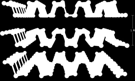
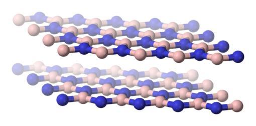
8 Black Phosphorus (bp) 1914: Bridgman produces first bp 1953: Keyes studies bp as a semiconductor 1968: Berman & Brandt; Witting & Mattias observe superconductivity at high pressure 1970 s s: burst of activity in Japan on electronic properties, Raman, cyclotron resonance 2014: ultra-thin bp FETs reported by Peide Ye (Purdue), Yuanbo Zhang (Fudan) and Jeanie Lau (UC Riverside) Puckered honeycomb layers Bulk band gap = 0.3 ev Monolayer band gap ~ 1.2 A. Morita, Semiconducting ev Black Phosphorus, Appl. Phys. A39, 227 (1986).
9 Black Phosphorus (bp) A. Morita, Semiconducting Black Phosphorus, Appl. Phys. A39, 227 (1986).
10 Black Phosphorus (bp) McGill University E E E p p p Schrödinger strain, electric field Dirac Xiang et al., Phys. Rev. Lett. 115, (2015)

11 bp Photo-oxidation: 20s of Ambient Air and Light Before After Rapid bp photo-oxidation with combination of O 2, H 2 O and light. A. Favron R. Martel, Photo-oxidation and quantum confinement effects in exfoliated black phosphorus, Nature Materials (2015).

12 Device Fabrication and Measurements


13 bp FET Fabrication : Top Approach Prof. Yuanbo Zhang, Fudan
 exfoliation & processing in glove box O 2, H")

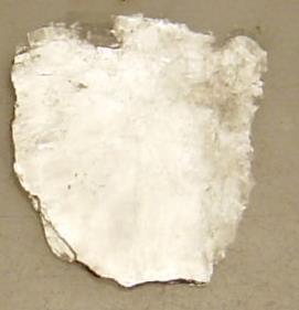
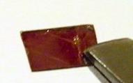
14 bp FET Fabrication : a Poor Man s Approach bulk bp source: 99.98% purity (Smart Elements) exfoliation & processing in glove box O 2, H 2 O < 1ppm 10μm 10μm e-beam lithography & Ti/Au contacts encapsulation with MMA/PMMA avoid simultaneous O 2, H 2 O, and Our best mobility: light ~1000 cm 2 /V.s
 V g =-27 V -37.5 180-80 -40 0 40 80 V g (V) -60-30 0 30 60 V g (V) 25 30 35 82±4 layers 1 7 6 5 4 0 5-50 -62.5-75 -87.5-100 V. Tayari, G. Gervais, R. Martel, T.")
15 R xx (k ) R (M ) R 2P (k ) (e) 90±2 layers (b) (c) Shubnikov de Haas Oscillations Source (d) (f) Drain (a) (c) PMMA 5 MMA 4 SiO 2 Si V g =-37.5 V T(K) B (T) V g =-27 V V g (V) V g (V) ±4 layers V. Tayari, G. Gervais, R. Martel, T. Szkopek Nature Communications ( B (T)
16 R xx ( ) R xx ( ) ) 50 0 Temperature -50 Dependence of SdH /B (T -1 ) T (K) (e) 60 B (T) Lifshitz- Kosevich: Damping: /B (T -1 ) T (K) m*=0.36 +/ m 0 V. Tayari, G. Gervais, R. Martel, T. Szkopek Nature Communications (2015

17 Independent Findings
18 Independent work regarding SdH Jeanie UC Riverside: N. Gillgren et al., Gate tuneable quantum oscillations in air-stable and high-mobility few-layer phosphorene heterostructures, 2D Materials Yuanbo Fudan: L. Li et al., Quantum oscillations in black phosphorus two-dimensional electron gas, Nature Nanotechnology Ning HKUST: X. Chen et al., High quality sandwiched black phosphorus heterostructure and its quantum oscillations, Nature Communications McGill + UdeM team: V. Tayari et al., Two dimensional magnetotransport in a naked black phosphorus quantum well, Nature Communications 2015.

19 New Developments in Bp: Device Engineering


20 Dual Gated Velocity Modulator (Engineering) V. Tayari, G. Gervais, T. Szkopek Phys. Rev. Applied 5, (2015)
21 See Talk by Prof. ICPS Monday 14h: 2D Materials beyond graphene (Mo-E3)

22 New Developments in Bp: Dephasing
23 Recent Work on Weak Localization in bp (Purdue)
24 Weak Localization in bp (McGill/Pisa)
25 Weak Localization in bp (McGill-Pisa)
26 Hikami-Larkin-Nagaoka (HLN) Theory WL correction to conductivity in 2D: with field parameters given by: where B 0 describes the elastic and Bf the inelastic (dephasing) scattering.
27 HLN Lengthscale and Timescales Scattering length L i associated with a field B i : and correspondingly the dephasing time t n is: where D is the elastic coefficient diffusion.
28 HLN Fits (at 0.26K)
29 HLN Fits (at 10K)
30 Temperature Dependence of Dephasing Length Lf
31 L f (nm) Dephasing in 2D Electron-electron scattering in the presence of elastic scattering in Graphene - A Graphene - B T -1/ T (K)
32 Temperature Dependence of Dephasing Length Lf

33 So, to conclude


34 Some Thoughts A Puckered Graphene experiment. Dephasing length/time more robust than what is expected in 2D. Anisotropy? 1D-like chain?

35 どうもありがとうございます Doumo arigatou gozaimasu
36 Temperature Dependence of Dephasing Length
37 Temperature Dependence of Dephasing Length

38 Temperature Dependence of Dephasing Length

39 Zero-field Transport 12.5±1 nm 24±2 layers 47±1 nm 90±2 layers
40 LL Index, N (b) Landau 1/B (TLevel -1 ) Fan Diagram Analysis b Hall bar V g = -50V V g = -100V Berry phase: F B =0 (c) /B (T -1 ) 0.06 two-terminal Hall bar holes = Schrödinger fermions V g (V) V. Tayari, G. Gervais, R. Martel, T. Szkopek Nature Communications (2015
41 bp FET Fabrication : a Much Better Approach Prof. Yuanbo Zhang Prof. Yuanbo Zhang best mobility: ~6000 cm 2 /V.s
42 More Temperature Dependence of SdH Prof. Yuanbo Zhang m*=0.34 m 0 F B =0 Nature Nanotechnology (2015)
 (b) (c) 4μm 8μm 8μm")


43 Atomic Force Microscopy (a) (b) (c) 4μm 8μm 8μm 6±1 nm 12.5±1 nm 47±1 nm 11±2 layers 24±2 layers 90±2 layers AFM performed after electrical transport measurements
44 2D Character from Angle-Resolved Data Prof. Yuanbo Zhang Nature Nanotechnology (2015)
 model: 3D (Fermi sphere)")
45 Fermi Surface and Carrier Density 2D (Fermi disc) model: 3D (Fermi sphere) model:
46 Schrödinger-Poisson Simulation Self-consistent Schrödinger-Poisson simulation: 2D hole accumulation layer rms width 2.7nm 5-6 layers E 1 - E 2 = 28 mev sub-band confinement energy V. Tayari, G. Gervais, R. Martel, T. Szkopek Nature Communications (2015
Black Phosphorus Field Effect Transistors: Passivation By Oxidation, and the Role of Anisotropy in Magnetotransport
 Black Phosphorus Field Effect Transistors: Passivation By Oxidation, and the Role of Anisotropy in Magnetotransport Tomasz Szkopek Electrical and Computer Engineering, Physics 231 st ECS Meeting, 1 June
Supplementary Information
 Supplementary Information Supplementary Figure 1 AFM and Raman characterization of WS 2 crystals. (a) Optical and AFM images of a representative WS 2 flake. Color scale of the AFM image represents 0-20
(a) (b) Supplementary Figure 1. (a) (b) (a) Supplementary Figure 2. (a) (b) (c) (d) (e)
 (b) Supplementary Figure 1. (a) (b) (a) Supplementary Figure 2. (a) (b) (c) (d) (e)") (a) (b) Supplementary Figure 1. (a) An AFM image of the device after the formation of the contact electrodes and the top gate dielectric Al 2 O 3. (b) A line scan performed along the white dashed line
(a) (b) Supplementary Figure 1. (a) An AFM image of the device after the formation of the contact electrodes and the top gate dielectric Al 2 O 3. (b) A line scan performed along the white dashed line
Dirac fermions in Graphite:
 Igor Lukyanchuk Amiens University, France, Yakov Kopelevich University of Campinas, Brazil Dirac fermions in Graphite: I. Lukyanchuk, Y. Kopelevich et al. - Phys. Rev. Lett. 93, 166402 (2004) - Phys. Rev.
A BIT OF MATERIALS SCIENCE THEN PHYSICS
 GRAPHENE AND OTHER D ATOMIC CRYSTALS Andre Geim with many thanks to K. Novoselov, S. Morozov, D. Jiang, F. Schedin, I. Grigorieva, J. Meyer, M. Katsnelson A BIT OF MATERIALS SCIENCE THEN PHYSICS CARBON
Supplementary Figure S1. AFM images of GraNRs grown with standard growth process. Each of these pictures show GraNRs prepared independently,
 Supplementary Figure S1. AFM images of GraNRs grown with standard growth process. Each of these pictures show GraNRs prepared independently, suggesting that the results is reproducible. Supplementary Figure
Bridging the Gap: Black Phosphorus for Electronics and Photonics
 IBM Thomas J. Watson Research Center Bridging the Gap: Black Phosphorus for Electronics and Photonics Fengnian Xia Department of Electrical Engineering Yale University, New Haven CT 06511 Email: fengnian.ia@yale.edu
1. Nanotechnology & nanomaterials -- Functional nanomaterials enabled by nanotechnologies.
 Novel Nano-Engineered Semiconductors for Possible Photon Sources and Detectors NAI-CHANG YEH Department of Physics, California Institute of Technology 1. Nanotechnology & nanomaterials -- Functional nanomaterials
Black phosphorus: A new bandgap tuning knob
 Black phosphorus: A new bandgap tuning knob Rafael Roldán and Andres Castellanos-Gomez Modern electronics rely on devices whose functionality can be adjusted by the end-user with an external knob. A new
2D Materials Research Activities at the NEST lab in Pisa, Italy. Stefan Heun NEST, Istituto Nanoscienze-CNR and Scuola Normale Superiore, Pisa, Italy
 2D Materials Research Activities at the NEST lab in Pisa, Italy Stefan Heun NEST, Istituto Nanoscienze-CNR and Scuola Normale Superiore, Pisa, Italy 2D Materials Research Activities at the NEST lab in
The BTE with a High B-field
 ECE 656: Electronic Transport in Semiconductors Fall 2017 The BTE with a High B-field Mark Lundstrom Electrical and Computer Engineering Purdue University West Lafayette, IN USA 10/11/17 Outline 1) Introduction
Carbon based Nanoscale Electronics
 Carbon based Nanoscale Electronics 09 02 200802 2008 ME class Outline driving force for the carbon nanomaterial electronic properties of fullerene exploration of electronic carbon nanotube gold rush of
Black phosphorus field-effect transistors
 SUPPLEMENTARY INFORMATION DOI: 10.1038/NNANO.2014.35 Black phosphorus field-effect transistors Likai Li, Yijun Yu, Guo Jun Ye, Qingqin Ge, Xuedong Ou, Hua Wu, Donglai Feng, Xian Hui Chen and Yuanbo Zhang
Electrostatics of Nanowire Transistors
 Electrostatics of Nanowire Transistors Jing Guo, Jing Wang, Eric Polizzi, Supriyo Datta and Mark Lundstrom School of Electrical and Computer Engineering Purdue University, West Lafayette, IN, 47907 ABSTRACTS
Chun Ning Lau (Jeanie) Quantum Transport! in! 2D Atomic Membranes!
 Quantum Transport! in! 2D Atomic Membranes!") Chun Ning Lau (Jeanie) Quantum Transport! in! 2D Atomic Membranes! 2D Materials and Heterostructures! hbn MoS 2 WSe 2 Fluorographene Geim, Nature 2013. Conductors, e.g. graphene, few-layer graphene Semiconductors,
Chun Ning Lau (Jeanie) Quantum Transport! in! 2D Atomic Membranes! 2D Materials and Heterostructures! hbn MoS 2 WSe 2 Fluorographene Geim, Nature 2013. Conductors, e.g. graphene, few-layer graphene Semiconductors,
Classification of Solids
 Classification of Solids Classification by conductivity, which is related to the band structure: (Filled bands are shown dark; D(E) = Density of states) Class Electron Density Density of States D(E) Examples
Graphene. Tianyu Ye November 30th, 2011
 Graphene Tianyu Ye November 30th, 2011 Outline What is graphene? How to make graphene? (Exfoliation, Epitaxial, CVD) Is it graphene? (Identification methods) Transport properties; Other properties; Applications;
GRAPHENE the first 2D crystal lattice
 GRAPHENE the first 2D crystal lattice dimensionality of carbon diamond, graphite GRAPHENE realized in 2004 (Novoselov, Science 306, 2004) carbon nanotubes fullerenes, buckyballs what s so special about
Optimizing Graphene Morphology on SiC(0001)
") Optimizing Graphene Morphology on SiC(0001) James B. Hannon Rudolf M. Tromp Graphene sheets Graphene sheets can be formed into 0D,1D, 2D, and 3D structures Chemically inert Intrinsically high carrier mobility
Optimizing Graphene Morphology on SiC(0001) James B. Hannon Rudolf M. Tromp Graphene sheets Graphene sheets can be formed into 0D,1D, 2D, and 3D structures Chemically inert Intrinsically high carrier mobility
Ferromagnetism and Anomalous Hall Effect in Graphene
 Ferromagnetism and Anomalous Hall Effect in Graphene Jing Shi Department of Physics & Astronomy, University of California, Riverside Graphene/YIG Introduction Outline Proximity induced ferromagnetism Quantized
2D-BLACK PHOSPHORUS FUNCTIONALIZED WITH METAL NANOPARTICLES: FULL CHARACTERIZATION AND CATALYTIC ACTIVITY ON HYDROGENATION REACTIONS
 2D-BLACK PHOSPHORUS FUNCTIONALIZED WITH METAL NANOPARTICLES: FULL CHARACTERIZATION AND CATALYTIC ACTIVITY ON HYDROGENATION REACTIONS EWPC-13 Freie Universität Berlin Salvatore Interlandi CNR-ICCOM Sesto
vapour deposition. Raman peaks of the monolayer sample grown by chemical vapour
 Supplementary Figure 1 Raman spectrum of monolayer MoS 2 grown by chemical vapour deposition. Raman peaks of the monolayer sample grown by chemical vapour deposition (S-CVD) are peak which is at 385 cm
Supporting Information
 Electronic Supplementary Material (ESI) for Nanoscale. This journal is The Royal Society of Chemistry 2015 Supporting Information Single Layer Lead Iodide: Computational Exploration of Structural, Electronic
Transport through Andreev Bound States in a Superconductor-Quantum Dot-Graphene System
 Transport through Andreev Bound States in a Superconductor-Quantum Dot-Graphene System Nadya Mason Travis Dirk, Yung-Fu Chen, Cesar Chialvo Taylor Hughes, Siddhartha Lal, Bruno Uchoa Paul Goldbart University
Graphene: Plane and Simple Electrical Metrology?
 Graphene: Plane and Simple Electrical Metrology? R. E. Elmquist, F. L. Hernandez-Marquez, M. Real, T. Shen, D. B. Newell, C. J. Jacob, and G. R. Jones, Jr. National Institute of Standards and Technology,
V bg
 SUPPLEMENTARY INFORMATION a b µ (1 6 cm V -1 s -1 ) 1..8.4-3 - -1 1 3 mfp (µm) 1 8 4-3 - -1 1 3 Supplementary Figure 1: Mobility and mean-free path. a) Drude mobility calculated from four-terminal resistance
Physics in two dimensions in the lab
 Physics in two dimensions in the lab Nanodevice Physics Lab David Cobden PAB 308 Collaborators at UW Oscar Vilches (Low Temperature Lab) Xiaodong Xu (Nanoscale Optoelectronics Lab) Jiun Haw Chu (Quantum
A. Optimizing the growth conditions of large-scale graphene films
 1 A. Optimizing the growth conditions of large-scale graphene films Figure S1. Optical microscope images of graphene films transferred on 300 nm SiO 2 /Si substrates. a, Images of the graphene films grown
SUPPLEMENTARY INFORMATION
 SUPPLEMENTARY INFORMATION SUPPLEMENTARY INFORMATION Trilayer graphene is a semimetal with a gate-tuneable band overlap M. F. Craciun, S. Russo, M. Yamamoto, J. B. Oostinga, A. F. Morpurgo and S. Tarucha
Graphite, graphene and relativistic electrons
 Graphite, graphene and relativistic electrons Introduction Physics of E. graphene Y. Andrei Experiments Rutgers University Transport electric field effect Quantum Hall Effect chiral fermions STM Dirac
Transport Experiments on 3D Topological insulators
 TheoryWinter School, NHMFL, Jan 2014 Transport Experiments on 3D Topological insulators Part I N. P. Ong, Princeton Univ. 1. Transport in non-metallic Bi2Se3 and Bi2Te3 2. A TI with very large bulk ρ Bi2Te2Se
High quality sandwiched black phosphorus heterostructure and its quantum oscillations
 High quality sandwiched black phosphorus heterostructure and its quantum oscillations Xiaolong Chen 1,, Yingying Wu 1,, Zefei Wu 1, Shuigang Xu 1, Lin Wang 2, Yu Han 1, Weiguang Ye 1, Tianyi Han 1, Yuheng
Monolayer Semiconductors
 Monolayer Semiconductors Gilbert Arias California State University San Bernardino University of Washington INT REU, 2013 Advisor: Xiaodong Xu (Dated: August 24, 2013) Abstract Silicon may be unable to
Anisotropic spin splitting in InGaAs wire structures
 Available online at www.sciencedirect.com Physics Physics Procedia Procedia 3 (010) 00 (009) 155 159 000 000 14 th International Conference on Narrow Gap Semiconductors and Systems Anisotropic spin splitting
Universal low-temperature Ohmic contacts for quantum transport in transition metal dichalcogenides
 2D Materials LETTER OPEN ACCESS Universal low-temperature Ohmic contacts for quantum transport in transition metal dichalcogenides To cite this article: Shuigang Xu et al 2016 2D Mater. 3 021007 View the
Supplementary Materials for
 advances.sciencemag.org/cgi/content/full/4/9/eaat8355/dc1 Supplementary Materials for Electronic structures and unusually robust bandgap in an ultrahigh-mobility layered oxide semiconductor, Bi 2 O 2 Se
Surfaces, Interfaces, and Layered Devices
 Surfaces, Interfaces, and Layered Devices Building blocks for nanodevices! W. Pauli: God made solids, but surfaces were the work of Devil. Surfaces and Interfaces 1 Interface between a crystal and vacuum
Supporting Information
 Supporting Information Monolithically Integrated Flexible Black Phosphorus Complementary Inverter Circuits Yuanda Liu, and Kah-Wee Ang* Department of Electrical and Computer Engineering National University
SUPPLEMENTARY INFORMATION
 DOI: 1.138/NNANO.211.214 Control over topological insulator photocurrents with light polarization J.W. McIver*, D. Hsieh*, H. Steinberg, P. Jarillo-Herrero and N. Gedik SI I. Materials and device fabrication
Graphene Novel Material for Nanoelectronics
 Graphene Novel Material for Nanoelectronics Shintaro Sato Naoki Harada Daiyu Kondo Mari Ohfuchi (Manuscript received May 12, 2009) Graphene is a flat monolayer of carbon atoms with a two-dimensional honeycomb
TRANSVERSE SPIN TRANSPORT IN GRAPHENE
 International Journal of Modern Physics B Vol. 23, Nos. 12 & 13 (2009) 2641 2646 World Scientific Publishing Company TRANSVERSE SPIN TRANSPORT IN GRAPHENE TARIQ M. G. MOHIUDDIN, A. A. ZHUKOV, D. C. ELIAS,
SUPPLEMENTARY INFORMATION
 Dirac electron states formed at the heterointerface between a topological insulator and a conventional semiconductor 1. Surface morphology of InP substrate and the device Figure S1(a) shows a 10-μm-square
Overview. Carbon in all its forms. Background & Discovery Fabrication. Important properties. Summary & References. Overview of current research
 Graphene Prepared for Solid State Physics II Pr Dagotto Spring 2009 Laurene Tetard 03/23/09 Overview Carbon in all its forms Background & Discovery Fabrication Important properties Overview of current
Supplementary Figure 1 Dark-field optical images of as prepared PMMA-assisted transferred CVD graphene films on silicon substrates (a) and the one
 and the one") Supplementary Figure 1 Dark-field optical images of as prepared PMMA-assisted transferred CVD graphene films on silicon substrates (a) and the one after PBASE monolayer growth (b). 1 Supplementary Figure
Supplementary Figure 1 Dark-field optical images of as prepared PMMA-assisted transferred CVD graphene films on silicon substrates (a) and the one after PBASE monolayer growth (b). 1 Supplementary Figure
2D MBE Activities in Sheffield. I. Farrer, J. Heffernan Electronic and Electrical Engineering The University of Sheffield
 2D MBE Activities in Sheffield I. Farrer, J. Heffernan Electronic and Electrical Engineering The University of Sheffield Outline Motivation Van der Waals crystals The Transition Metal Di-Chalcogenides
SUPPLEMENTARY INFORMATION
 DOI: 1.138/NMAT3449 Topological crystalline insulator states in Pb 1 x Sn x Se Content S1 Crystal growth, structural and chemical characterization. S2 Angle-resolved photoemission measurements at various
Valley Hall effect in electrically spatial inversion symmetry broken bilayer graphene
 NPSMP2015 Symposium 2015/6/11 Valley Hall effect in electrically spatial inversion symmetry broken bilayer graphene Yuya Shimazaki 1, Michihisa Yamamoto 1, 2, Ivan V. Borzenets 1, Kenji Watanabe 3, Takashi
Observation of topological surface state quantum Hall effect in an intrinsic three-dimensional topological insulator
 Observation of topological surface state quantum Hall effect in an intrinsic three-dimensional topological insulator Authors: Yang Xu 1,2, Ireneusz Miotkowski 1, Chang Liu 3,4, Jifa Tian 1,2, Hyoungdo
Quantum Confinement in Graphene
 Quantum Confinement in Graphene from quasi-localization to chaotic billards MMM dominikus kölbl 13.10.08 1 / 27 Outline some facts about graphene quasibound states in graphene numerical calculation of
Hybrid Graphene Quantum Dot Devices and Their Applications
 Hybrid Graphene Quantum Dot Devices and Their Applications Eric Law Department of Electrical and Computer Engineering University of California, Davis Davis, CA 95616 Term Paper for EEC 247: Advanced Semiconductors
Supplementary Figure 1 Magneto-transmission spectra of graphene/h-bn sample 2 and Landau level transition energies of three other samples.
 Supplementary Figure 1 Magneto-transmission spectra of graphene/h-bn sample 2 and Landau level transition energies of three other samples. (a,b) Magneto-transmission ratio spectra T(B)/T(B 0 ) of graphene/h-bn
Identifying the crystal orientation of the black phosphorus
 Identifying the crystal orientation of the black phosphorus Yu ZHANG I. Introduction Black phosphorus is a new member of 2D materials family. It has several noticeable properties, for instance, the direct
Self-assembled SiGe single hole transistors
 Self-assembled SiGe single hole transistors G. Katsaros 1, P. Spathis 1, M. Stoffel 2, F. Fournel 3, M. Mongillo 1, V. Bouchiat 4, F. Lefloch 1, A. Rastelli 2, O. G. Schmidt 2 and S. De Franceschi 1 1
SUPPLEMENTARY INFORMATION
 Dirac cones reshaped by interaction effects in suspended graphene D. C. Elias et al #1. Experimental devices Graphene monolayers were obtained by micromechanical cleavage of graphite on top of an oxidized
NONLINEAR TRANSPORT IN BALLISTIC SEMICONDUCTOR DIODES WITH NEGATIVE EFFECTIVE MASS CARRIERS
 NONLINEAR TRANSPORT IN BALLISTIC SEMICONDUCTOR DIODES WITH NEGATIVE EFFECTIVE MASS CARRIERS B. R. Perkins, Jun Liu, and A. Zaslavsky, Div. of Engineering Brown University Providence, RI 02912, U.S.A.,
Spin Orbit Coupling (SOC) in Graphene
 in Graphene") Spin Orbit Coupling (SOC) in Graphene MMM, Mirko Rehmann, 12.10.2015 Motivation Weak intrinsic SOC in graphene: [84]: Phys. Rev. B 80, 235431 (2009) [85]: Phys. Rev. B 82, 125424 (2010) [86]: Phys. Rev.
Spin Orbit Coupling (SOC) in Graphene MMM, Mirko Rehmann, 12.10.2015 Motivation Weak intrinsic SOC in graphene: [84]: Phys. Rev. B 80, 235431 (2009) [85]: Phys. Rev. B 82, 125424 (2010) [86]: Phys. Rev.
Surface atoms/molecules of a material act as an interface to its surrounding environment;
 1 Chapter 1 Thesis Overview Surface atoms/molecules of a material act as an interface to its surrounding environment; their properties are often complicated by external adsorbates/species on the surface
Rectification in a Black Phosphorus/WS2 van der. Waals Heterojunction Diode
 Supporting Information Temperature-Dependent and Gate-Tunable Rectification in a Black Phosphorus/WS2 van der Waals Heterojunction Diode Ghulam Dastgeer 1, Muhammad Farooq Khan 1, Ghazanfar Nazir 1, Amir
Supplementary information for Tunneling Spectroscopy of Graphene-Boron Nitride Heterostructures
 Supplementary information for Tunneling Spectroscopy of Graphene-Boron Nitride Heterostructures F. Amet, 1 J. R. Williams, 2 A. G. F. Garcia, 2 M. Yankowitz, 2 K.Watanabe, 3 T.Taniguchi, 3 and D. Goldhaber-Gordon
Supplementary Figures
 Supplementary Figures Supplementary Figure 1. Crystal structure of 1T -MoTe 2. (a) HAADF-STEM image of 1T -MoTe 2, looking down the [001] zone (scale bar, 0.5 nm). The area indicated by the red rectangle
Tuning Rashba Spin-Orbit Coupling in Gated Multi-layer InSe
 Supporting Information Tuning Rashba Spin-Orbit Coupling in Gated Multi-layer InSe Kasun Premasiri, Santosh Kumar Radha, Sukrit Sucharitakul, U. Rajesh Kumar, Raman Sankar,, Fang-Cheng Chou, Yit-Tsong
Intrinsic Electronic Transport Properties of High. Information
 Intrinsic Electronic Transport Properties of High Quality and MoS 2 : Supporting Information Britton W. H. Baugher, Hugh O. H. Churchill, Yafang Yang, and Pablo Jarillo-Herrero Department of Physics, Massachusetts
Interference of magnetointersubband and phonon-induced resistance oscillations in single GaAs quantum wells with two populated subbands
 Interference of magnetointersubband and phonon-induced resistance oscillations in single GaAs quantum wells with two populated subbands A.A.Bykov and A.V.Goran Institute of Semiconductor Physics, Russian
Hybrid Surface-Phonon-Plasmon Polariton Modes in Graphene /
 Supplementary Information: Hybrid Surface-Phonon-Plasmon Polariton Modes in Graphene / Monolayer h-bn stacks Victor W. Brar 1,2, Min Seok Jang 3,, Michelle Sherrott 1, Seyoon Kim 1, Josue J. Lopez 1, Laura
POLARIZATION INDUCED EFFECTS IN AlGaN/GaN HETEROSTRUCTURES
 Vol. 98 (2000) ACTA PHYSICA POLONICA A No. 3 Proceedings of the XXIX International School of Semiconducting Compounds, Jaszowiec 2000 POLARIZATION INDUCED EFFECTS IN AlGaN/GaN HETEROSTRUCTURES O. AMBACHER
Electronic structure and properties of a few-layer black phosphorus Mikhail Katsnelson
 Electronic structure and properties of a few-layer black phosphorus Mikhail Katsnelson Main collaborators: Sasha Rudenko Shengjun Yuan Rafa Roldan Milton Pereira Sergey Brener Motivation Plenty of 2D materials
SUPPLEMENTARY INFORMATION
 doi:10.1038/nature13734 1. Gate dependence of the negatively charged trion in WS 2 monolayer. We test the trion with both transport and optical measurements. The trion in our system is negatively charged,
Supporting Information. by Hexagonal Boron Nitride
 Supporting Information High Velocity Saturation in Graphene Encapsulated by Hexagonal Boron Nitride Megan A. Yamoah 1,2,, Wenmin Yang 1,3, Eric Pop 4,5,6, David Goldhaber-Gordon 1 * 1 Department of Physics,
Quantum Condensed Matter Physics Lecture 17
 Quantum Condensed Matter Physics Lecture 17 David Ritchie http://www.sp.phy.cam.ac.uk/drp/home 17.1 QCMP Course Contents 1. Classical models for electrons in solids. Sommerfeld theory 3. From atoms to
Fermi polaron-polaritons in MoSe 2
 Fermi polaron-polaritons in MoSe 2 Meinrad Sidler, Patrick Back, Ovidiu Cotlet, Ajit Srivastava, Thomas Fink, Martin Kroner, Eugene Demler, Atac Imamoglu Quantum impurity problem Nonperturbative interaction
Supplementary Information for
 Supplementary Information for Highly Stable, Dual-Gated MoS 2 Transistors Encapsulated by Hexagonal Boron Nitride with Gate-Controllable Contact Resistance and Threshold Voltage Gwan-Hyoung Lee, Xu Cui,
arxiv: v2 [cond-mat.mtrl-sci] 4 Dec 2015
![arxiv: v2 [cond-mat.mtrl-sci] 4 Dec 2015](/thumbs/90/102189380.jpg "arxiv: v2 [cond-mat.mtrl-sci] 4 Dec 2015") Pressure-Induced Electronic Transition in Black Phosphorus arxiv:1.1v [cond-mat.mtrl-sci] Dec 1 Z. J. Xiang 1, G. J. Ye 1, C. Shang 1, B. Lei 1, N. Z. Wang 1, K. S. Yang, D. Y. Liu, F. B. Meng 1, X. G.
Pressure-Induced Electronic Transition in Black Phosphorus arxiv:1.1v [cond-mat.mtrl-sci] Dec 1 Z. J. Xiang 1, G. J. Ye 1, C. Shang 1, B. Lei 1, N. Z. Wang 1, K. S. Yang, D. Y. Liu, F. B. Meng 1, X. G.
SiC Graphene Suitable For Quantum Hall Resistance Metrology.
 SiC Graphene Suitable For Quantum Hall Resistance Metrology. Samuel Lara-Avila 1, Alexei Kalaboukhov 1, Sara Paolillo, Mikael Syväjärvi 3, Rositza Yakimova 3, Vladimir Fal'ko 4, Alexander Tzalenchuk 5,
Fermi Level Pinning at Electrical Metal Contacts. of Monolayer Molybdenum Dichalcogenides
 Supporting information Fermi Level Pinning at Electrical Metal Contacts of Monolayer Molybdenum Dichalcogenides Changsik Kim 1,, Inyong Moon 1,, Daeyeong Lee 1, Min Sup Choi 1, Faisal Ahmed 1,2, Seunggeol
GRAPHENE ON THE Si-FACE OF SILICON CARBIDE USER MANUAL
 GRAPHENE ON THE Si-FACE OF SILICON CARBIDE USER MANUAL 1. INTRODUCTION Silicon Carbide (SiC) is a wide band gap semiconductor that exists in different polytypes. The substrate used for the fabrication
Magneto-plasmonic effects in epitaxial graphene
 Magneto-plasmonic effects in epitaxial graphene Alexey Kuzmenko University of Geneva Graphene Nanophotonics Benasque, 4 March 13 Collaborators I. Crassee, N. Ubrig, I. Nedoliuk, J. Levallois, D. van der
Wafer-scale fabrication of graphene
 Wafer-scale fabrication of graphene Sten Vollebregt, MSc Delft University of Technology, Delft Institute of Mircosystems and Nanotechnology Delft University of Technology Challenge the future Delft University
Electrical Contacts to Carbon Nanotubes Down to 1nm in Diameter
 1 Electrical Contacts to Carbon Nanotubes Down to 1nm in Diameter Woong Kim, Ali Javey, Ryan Tu, Jien Cao, Qian Wang, and Hongjie Dai* Department of Chemistry and Laboratory for Advanced Materials, Stanford
SUPPLEMENTARY INFORMATION
 SUPPLEMENTARY INFORMATION DOI: 10.1038/NNANO.2011.138 Graphene Nanoribbons with Smooth Edges as Quantum Wires Xinran Wang, Yijian Ouyang, Liying Jiao, Hailiang Wang, Liming Xie, Justin Wu, Jing Guo, and
Graphene devices and integration: A primer on challenges
 Graphene devices and integration: A primer on challenges Archana Venugopal (TI) 8 Nov 2016 Acknowledgments: Luigi Colombo (TI) UT Dallas and UT Austin 1 Outline Where we are Issues o Contact resistance
Organic Electronic Devices
 Organic Electronic Devices Week 5: Organic Light-Emitting Devices and Emerging Technologies Lecture 5.5: Course Review and Summary Bryan W. Boudouris Chemical Engineering Purdue University 1 Understanding
2D Materials for Gas Sensing
 2D Materials for Gas Sensing S. Guo, A. Rani, and M.E. Zaghloul Department of Electrical and Computer Engineering The George Washington University, Washington DC 20052 Outline Background Structures of
Ferroelectric Field Effect Transistor Based on Modulation Doped CdTe/CdMgTe Quantum Wells
 Vol. 114 (2008) ACTA PHYSICA POLONICA A No. 5 Proc. XXXVII International School of Semiconducting Compounds, Jaszowiec 2008 Ferroelectric Field Effect Transistor Based on Modulation Doped CdTe/CdMgTe Quantum
NiCl2 Solution concentration. Etching Duration. Aspect ratio. Experiment Atmosphere Temperature. Length(µm) Width (nm) Ar:H2=9:1, 150Pa
 Width (nm) Ar:H2=9:1, 150Pa") Experiment Atmosphere Temperature #1 # 2 # 3 # 4 # 5 # 6 # 7 # 8 # 9 # 10 Ar:H2=9:1, 150Pa Ar:H2=9:1, 150Pa Ar:H2=9:1, 150Pa Ar:H2=9:1, 150Pa Ar:H2=9:1, 150Pa Ar:H2=9:1, 150Pa Ar:H2=9:1, 150Pa Ar:H2=9:1,
Experiment Atmosphere Temperature #1 # 2 # 3 # 4 # 5 # 6 # 7 # 8 # 9 # 10 Ar:H2=9:1, 150Pa Ar:H2=9:1, 150Pa Ar:H2=9:1, 150Pa Ar:H2=9:1, 150Pa Ar:H2=9:1, 150Pa Ar:H2=9:1, 150Pa Ar:H2=9:1, 150Pa Ar:H2=9:1,
Strong light matter coupling in two-dimensional atomic crystals
 SUPPLEMENTARY INFORMATION DOI: 10.1038/NPHOTON.2014.304 Strong light matter coupling in two-dimensional atomic crystals Xiaoze Liu 1, 2, Tal Galfsky 1, 2, Zheng Sun 1, 2, Fengnian Xia 3, Erh-chen Lin 4,
Tutorial T5 Will Carbon Replace Silicon? The future of graphitic electronics.
 Tutorial T5 Will Carbon Replace Silicon? The future of graphitic electronics. 1:30-2:20 Jim Meindl Nanoelectronics in Retrospect and Prospect 2:20-3:10 Millie Dresselhaus From Graphene to Graphite to Nanotubes
Lithography-Free Fabrication of High Quality Substrate- Supported and Freestanding Graphene Devices
 98 DOI 10.1007/s12274-010-1013-5 Research Article Lithography-Free Fabrication of High Quality Substrate- Supported and Freestanding Graphene Devices Wenzhong Bao 1, Gang Liu 1, Zeng Zhao 1, Hang Zhang
STM and graphene. W. W. Larry Pai ( 白偉武 ) Center for condensed matter sciences, National Taiwan University NTHU, 2013/05/23
 Center for condensed matter sciences, National Taiwan University NTHU, 2013/05/23") STM and graphene W. W. Larry Pai ( 白偉武 ) Center for condensed matter sciences, National Taiwan University NTHU, 2013/05/23 Why graphene is important: It is a new form of material (two dimensional, single
STM and graphene W. W. Larry Pai ( 白偉武 ) Center for condensed matter sciences, National Taiwan University NTHU, 2013/05/23 Why graphene is important: It is a new form of material (two dimensional, single
Supplementary Figures
 Supplementary Figures 1500 Heating Annealing Growing Cooling 20 Temperature ( o C) 1000 500 Ar:H 2 = 5:1 Ar:H 2 = 5:1 15 10 5 Pressure(Pa) 0 Ar(SiH 4 (5%)):C 2 H 2 = 1:2 120 mins 5 mins 5 40 mins ~120
SIMULATION OF A Si/SiGe MODULATION-DOPED FET USING QUANTUM HYDRODYNAMIC EQUATIONS*
 SIMULATION OF A Si/SiGe MODULATION-DOPED FET USING QUANTUM HYDRODYNAMIC EQUATIONS* J.-R. Zhou, T. Yamada, H. Miyata +, and D. K. Ferry Center for Solid State Electronics Research Arizona State University,
Ambipolar bistable switching effect of graphene
 Ambipolar bistable switching effect of graphene Young Jun Shin, 1,2 Jae Hyun Kwon, 1,2 Gopinadhan Kalon, 1,2 Kai-Tak Lam, 1 Charanjit S. Bhatia, 1 Gengchiau Liang, 1 and Hyunsoo Yang 1,2,a) 1 Department
SUPPLEMENTARY INFORMATION
 SUPPLEMENTARY INFORMATION DOI: 10.1038/NNANO.2011.123 Ultra-strong Adhesion of Graphene Membranes Steven P. Koenig, Narasimha G. Boddeti, Martin L. Dunn, and J. Scott Bunch* Department of Mechanical Engineering,
Quantum Oscillations in Graphene in the Presence of Disorder
 WDS'9 Proceedings of Contributed Papers, Part III, 97, 9. ISBN 978-8-778-- MATFYZPRESS Quantum Oscillations in Graphene in the Presence of Disorder D. Iablonskyi Taras Shevchenko National University of
Magneto-transport in MoS2: Phase Coherence, Spin-Orbit Scattering, and the Hall Factor
 Purdue University Purdue e-pubs Birck and NCN Publications Birck Nanotechnology Center 8-2013 Magneto-transport in MoS2: Phase Coherence, Spin-Orbit Scattering, and the Hall Factor Adam T. Neal Birck Nanotechnology
Magneto-transport Study of 3D Topological Insulator Bi2Te3 And GaAs/AlGaAs 2D Electron System
 Georgia State University ScholarWorks @ Georgia State University Physics and Astronomy Dissertations Department of Physics and Astronomy 8-8-2017 Magneto-transport Study of 3D Topological Insulator Bi2Te3
Supporting Information
 Electronic Supplementary Material (ESI) for ChemComm. This journal is The Royal Society of Chemistry 2014 Supporting Information Controllable Atmospheric Pressure Growth of Mono-layer, Bi-layer and Tri-layer
Oliver Portugall Laboratoire National des Champs Magnétiques Intenses (LNCMI) Toulouse & Grenoble, France
 Toulouse & Grenoble, France") Oliver Portugall Laboratoire National des Champs Magnétiques Intenses (LNCMI) Toulouse & Grenoble, France 1 Building & Infrastructure 2 3 Industrial building (steel panel construction) 6 explosion proof
Oliver Portugall Laboratoire National des Champs Magnétiques Intenses (LNCMI) Toulouse & Grenoble, France 1 Building & Infrastructure 2 3 Industrial building (steel panel construction) 6 explosion proof
Graphene A One-Atom-Thick Material for Microwave Devices
 ROMANIAN JOURNAL OF INFORMATION SCIENCE AND TECHNOLOGY Volume 11, Number 1, 2008, 29 35 Graphene A One-Atom-Thick Material for Microwave Devices D. DRAGOMAN 1, M. DRAGOMAN 2, A. A. MÜLLER3 1 University
Detection of Ionizing Radiations with Graphene Field Effect Transistors (GFET) Yong P. Chen Purdue University
 Yong P. Chen Purdue University") Detection of Ionizing Radiations with Graphene Field Effect Transistors (GFET) Yong P. Chen (yongchen@purdue.edu), Purdue University IEEE NSS 10/26/2009 Team Members: Isaac Childres, Mike Foxe, Gabriel
Detection of Ionizing Radiations with Graphene Field Effect Transistors (GFET) Yong P. Chen (yongchen@purdue.edu), Purdue University IEEE NSS 10/26/2009 Team Members: Isaac Childres, Mike Foxe, Gabriel
Topological 1T -phases patterned onto few-layer semiconducting-phase MoS2 by laser beam irradiation
 Topological 1T -phases patterned onto few-layer semiconducting-phase MoS2 by laser beam irradiation H. Mine 1, A. Kobayashi 1, T. Nakamura 2, T. Inoue 3, J. J. Palacios 4, E. Z. Marin 4, S. Maruyama 3,