Single Electron Transistor
|
|
|
- Godwin Fitzgerald
- 5 years ago
- Views:
Transcription
1 Single-Electron Transistors u Reference book: Single Charge Tunneling Coulomb Blockade Phenomena in Nanostructures By Hermann Grabertand Michel H. Devoret, 1992 u Referred Journal Review Papers: Correlated discrete transfer of single electrons in ultrasmalltunnel juntions By K. K. Likharev, IBM J. Res. Develop. Vol.32, p.144, 1989 Single-Electron Devices and Their Applications By K. K. Likharev, Proceedings of the IEEE, vol.87, p.606, 1999 Single-Electron Memory for Gita-to Tera Bit Storage By K. Yano et al., Proceedings of the IEEE, vol.87, p.633,
2 Contents u Single Electron Phenomena: A General Introduction u u Fabrication and Analysis u Applications 2
3 Single Electron Phenomena: A General Introduction u.scaling prospects for various bit-addressable memories. DRAM is expected to be bottlenecked at the generation of 64 Gbitintegration (70 nm technology) due to the problems with the storage capacitor scaling. Nonvolatile memory is going to be the mainstream for 64Gbit-16Tbit memory. SET/FET would be feasible starting from ~ 3 nm minimum feature sizes. 3
4 SET Evolution u The manipulation of single electrons was demonstrated in the seminal experiments by Millikanat the very beginning of 20 century. u Single Electron Device: in which the addition or substractionof a small number of electrons to/from an electrode can be controlled with one-electron precision using the charging effect. They are not interesting not only as new physical phenomena in nanostructures but also because they offer new operating principles for future ICs. Application: Memory, switch, Thermal meter u Advantages: Good stability: is the strong incentive to explore the possibility of the devices. atomic scale physical dimension ULSI possible Ultralowpower operation: simply because they use very small number of electrons to accomplish basic operation. Fast operation: only a few electrons (<100) are transferred, therefore, the charge/discharge process might be faster than those of conventional devices. (100,000 electrons) 4

5 Schematic of Single Electron Devices u A quantum dot is weakly coupled by tunnel barriers to two electron reserviors. Oxide 5
6 A General Introduction u Recall that the motion of electrons in an infinite potential well is in a standing waveform. That means that the energy of the particle in the infinite potential well is quantized. That is, the energy of the particle can only have particular discrete values h n π E = E n = 2 2ma where n is a positive integer 6
7 Charging Energy u Let a small conductor (island) be initially electroneutral, i.e., have exactly as many (m) electrons as it has protons in its crystal lattice. In this state the island does not generate any appreciable electric field beyond its borders, and a weak external force may bring in an additional electron from outside. Now the net charge of the island is (-e), and the resulting E field repulses the following electrons which might be added. 7
8 Charging Energy u The charging energy of the island is E C, where C is the capacitance of the island: 2 E e C = C u When the size of the island becomes comparable with the de Broglie wavelength of the electron inside the island energy quantization E ( n π h ) h k = + N 2 2 mw 2 m u The energy scale of the charging effects is given by a more general notion, the electron addition energy (E a ). In most cases of interest, E a could be approximated by E = E + E a C Here E k is the quantum kinetic energy of the addition electron; for a degenerate electron gas E k = 1/g(ε F )V, where V is the island volume and g(ε F ) is the density of states on the Fermi surface. k 8
9 Electron Transfer in an quantum dot u The transport of electrons through the quantum dots is an interplay of resonant tunneling and Coulomb blockade effects. u In the absence of charging effect, a conductance peak due to resonant tunneling occurs when the Fermi energy E F in the source lines up with one of the energy levels in the dot. E F = E n 2 2 h n π = 2 2 ma 2, where E is the bare energy level u However, this condition is modified by the charging effect. The energy level is renormalized by the charging effect 2 * 1 e E N E n + N, where E n is the bare level 2 C 2 e u That is, the renormalized level spacing E = E + C is enhanced above the bare level spacing by the charging energy. n 9
10 Single-electron tunneling through a quantum dot Bare Energy level Normalized Energy level E * = E + e 2 C The energy levels, E N, are modified by the charging effect. That is the charging energy regulates the level spacing. The spin degeneracy is lifted by the charging energy. 10
, with N referring to the lowest unoccupied level in E N e 2 = E 2 C")
11 Single-electron tunneling through a quantum dot (a) (b) E N 2 + e = E + e ( N 2 C F φ the dot. An electron has tunneled into the dot, 1 ), with N referring to the lowest unoccupied level in E N e 2 = E 2 C F + e φ ( N ) 11
12 Addition Energy, Kinetic Energy u For 100-nm-scale devices, E a is dominated by the charging energy E c and is of the order of 1 mev (~10 K). Since the thermal fluctuations suppress most single-electron effects unless E a 10kBT these device have to be operated in the sub-1-k range. Unpractical! u If the island size is below ~ 10 nm, E a approaches 100 mev, and some single electron effects become visible at RT. u However, digital SE devices require even higher values of E a to avoid thermally induced random tunneling events, so that minimum feature size of SET has to be smaller than ~ 1nm. RT operation E a = E C + E 12
13 u The resulting SET device is reminiscent of a usual MOSFET, but with a small conducting island embedded between two tunnel barriers, instead of the usual inversion channel. V g u The expression of the electrostatic energy W of this SET is W [ n C + n C ] C const 2 = ( ne Q e ) / 2 C total ev / total + n 1 and n 2 are the number of electrons passed through the tunnel barriers one and two, respectively, so that n = n 1 - n 2, while the total island capacitance C total is now a sum of C 0, C 1, C 2, and whatever stray capacitance the island may have. The external charge Q e = C 0 V g is just a convenient way to present the effect of the gate voltage V g. 13
14 (SET) u Operation principle: 14

15 I d -V d Characteristics u I d -V d is a function of V g. u Coulomb Blockade Threshold Voltage V th. Coulomb gap 15

16 Coulomb Gap u Large bias (V ds ) I d -V ds measurements generally probe the excitation spectrum of the dot. The conductance peaks are associated with the excited electron states in the QD, appearing whenever such an excitation is aligned with the Fermi level of one of the S/D leads. u The Coulomb-blockade gap is manifested by the flat region of the I d - V ds curve spanning V ds ~ 0V. At the edge of the gap, the large peak in differential conductance on either side marks the threshold voltage above which electrons can tunnel into the dot. Coulomb gap = V ds = ( C + C ) d e s 16
17 Coulomb Staircase u Unlike the Coulomb suppression of current in the neighborhood of V ds = 0 V (Coulomb gap), the staircase is not a universal feature of the Coulomb blockade. Rather, it is a special result of having very different tunneling rates through the two tunneling barriers. Coulomb staircase 17

18 Coulomb Staircase u Increasing V ds, the quasi-fermi level on Source lead is raised by the bias potential; initially no current flows because electrons at the quasi-fermilevel do not yet have enough energy to overcome the charging energy of the QD. u Eventually, V ds reaches the point at which an electron can tunnel from the Source lead onto the QD. current flow and a peak in G is observed. 18
19 Physics of Coulomb Staircase u Increasing gate voltage V g attracts more and more electrons to the island. The discreteness of electron transfer through low-transparency barriers necessarily makes this increase step like. u When one tunnel barrier is significantly more transmitting than the other tunnel barrier, the I-V behavior of the dot can exhibit the namely Coulomb staircase behavior, that is a stepwise curve. u What is surprising is that even such a simple device allows a reliable addition/subtraction of single electrons to/from an island with an enormous (and unknown) number of background electrons, of the order of one million in typical low-temperature experiments with 100-nm-scale aluminum islands. 19

20 I d -V g Characteristics u Coulomb-Blockade Oscillation in I d -V g and conductance-v g, where conductance I G = V d d 20
21 Conductance Positions u The gate-voltage position of the conductance peaks, corresponding to chargedegeneracy points, are determined at very low temperatures by the conditions E(N) = E(N+1), which leads to eϕ N+1 = (N+1/2)e 2 /C + ε N+1. (Recall that, where ε i represents the energy of the i th eigenstaterelative to the Fermi level in the QD and the summation is over the set of occupied states.) a u The spacing between conductance peaks V g = = +, where E a is the single-electron addition energy, e α C dot E is the Coulomb charging energy and is the quantized level separation. The gate-voltage position of the conductance peaks contains information about the single-particle energies. (addition energy, charging energy, and quantized level separation) E ( N ) = ( Ne) 2 C 2 ϕ Ne + ε 21 N i E α e e α C dot E α e

22 Conductance Positions u In principle, unless the single-particle levels ε I are equally spaced, the conductance peaks are not exactly periodic in V g. This is true as long as kt << E, for which peaks are narrow enough to resolve the contribution of. u However, as long as the charging energy is larger than the levelspacing, as is often the case in the planar QDs that are a few hundred nm in size, the deviations from periodicity are relatively small. 22 g
23 Temperature Behavior of Conductance Peaks u At low temperatures, the heights of successive peaks in V g vary non-monotonically and adjacent peaks are separated by broad minima. when kt << E, the conductance of any particular peak is entirely determined by the tunneling rates Γ i l and Γ i r of a specific single particle state i. Large-amplitude peaks are associated with states that are more strongly coupled to the source or drain leads; low-amplitude peaks with weakly coupled states. u As the temperature is increased, all thepeaks are broaden; their amplitudes decrease in some cases and increase in other cases; in certain cases (the peak shown furthest to the right), the amplitude first decreases then increases as the temperature is raised. As temperature is increased and kt ~ E, each conductance peak is influenced by contributions of tunneling through several discrete energy states, although still within the constraint of one electron at a time. The monotonic increase in peak amplitudes at high temperatures simply reflects the trend towards more strongly coupled levels at higher V g. The coefficient α can be determined from the temperature dependence of the peak s full width at halfmaximum: FWHM = 3.5kT/(αe) 2. u Eventually, at the highest temperature, peak overlap significantly and the amplitude of successive peaks in V g increases monotonically. 23
/C g G < 0 Fine structure 24")
24 Rhombus Shapes in the Contour Plot of differential conductance S 1 V g / V d =C d /C g S 2 V g / V d =(C s +C g )/C g G < 0 Fine structure 24
25 Device Parameters Extracted from the Rhombus Shapes u The electronic structure in the QD could be extracted from the contour plot of the differential conductance as a function of V g and V d. u The ratio of the gate-dot (C g ), drain-dot (C d ), and source-dot (C s ) capacitances can be calculated from the slope S 1 and S 2. C g : C d : C s = 1: S 1 : S 2 u Then the gain modulation α C g /C total, C total = C g + C d + C s u The addition energy E a = α V g. 25
26 Electronic Structure extracted from I-V u Addition Energy u Charging Energy u Energy level spacing u Dot diameter 26
27 Minimum tunneling resistance for single-electron charging u Implicit in the formulation of the Coulomb-blockade model is the condition that the number of electrons localized in the dot island, N, is a well-defined integer. This is to say, well defined in the classical sense, as opposed to a quantum definition which describes N in terms of an average value <N>, which is not necessarily an integer, and time-averaged fluctuations <δn 2 >. u The Coulomb-blockade model requires that <δn 2 > << 1. Clearly, if the tunnel barriers are not present, or are insufficiently opaque, nothing will constrain a quantized electronic charge to be confined within a certain volume. A general view is that there is a minimum resistance which the barriers must exceed in order to have <δn 2 > << 1, and this resistance is of the order of the quantum resistance R K = h/e 2 = 25,813 Ω. u The condition <δn 2 > << 1 requires that the time that an electron resides on the dot, τ, be much greater than δτ, the quantum uncertainty in this time. The current I cannot exceed e/τ since no more than one extra electron resides on the dot at any instant. The energy uncertainty of the electron, δe, is no larger than the applied voltage, hence the condition that δτ << τ translates into macroscopic variables using I e/τ, δτδe h and δe < ev ds. Doing so gives the minimum tunneling resistance condition, R K = V ds /I h/e 2. 27
28 Co-tunneling u Even if the minimum resistance criterion is met and single-electron charging effects are manifested, small quantum fluctuations, or uncertainties, in N are not entirely ruled out. In the classical Coulomb-blockade model there is then a fixed number of electrons N on the QD and at T= 0 the charge on the QD does not fluctuate. u However, the fact that very small quantum fluctuation in N may be present corresponds to electrons momentarily tunneling onto the QD, with an energy deficit on the scale of the classical Coulomb charging energy. u Essentially, the tunneling electron resides on the QD in a virtual charge state for a sufficiently brief interval such that the energy uncertainty of this state is larger than its classical energy deficit, subsequently tunneling out. This process has been referred to as co-tunneling or macroscopic quantum tunneling of charge. u The rational behind is that the total charge of the system (a macroscopic variable) undergoes a transition through a classically forbiddenintermediate state, in apparent violation of the Coulomb blockade. 28
29 Elastic co-tunneling u The tunneling of an electron into a certain energy state and the tunneling of an electron from the same state out of the dot. The end result of the two tunneling events is that the state of the QD is unchanged, and as such, this is referred to as elastic co-tunneling, which contributes a linear term to the I-V curve. I el = h σ σ 8 π e 1 E E 2 where is the average energy separation between eigenstates in the QD and E 1 (E 2 ) is the charging energy associated with adding (removing) a single electron to (from) the dot. Note, in particular, that the resulting conductance scales roughly as the ratio between the level spacing and the Coulomb gap U e 2 /C. u The case of elastic co-tunneling depends, in principle, on the geometry of the QD. This is because the electron involved has to couple to both leads; thus in a sense it must traverse the dot in a virtual state. V 29
30 Inelastic co-tunneling u It corresponds to an electron tunnels into a certain state in the dot and a second electron, from a different state, tunnels out of the dot. The state of the dot is modified, leaving an electron-hole excitation. The resulting current is nonlinear in V ds and temperature-dependent. The case of inelastic co-tunneling gives the following well-known form I inel 2 h σ ev = 1 σ e E E π 2 2 ( kt ) + V 30
31 Cotunneling u The distinction is made between these two processes because their relative contributions to the total net cotunneling current depend on the density of states in the QD. u In metal QDs, in which the density of states is large, the elastic component of co-tunneling is usually overwhelmed by the inelastic component. u In semiconductor QDs, in which the density of states is much smaller than in metals, both elastic and inelastic terms can contribute to the co-tunneling current. u In practice, co-tunneling is expected to modify the classical picture of singleelectron charging in the form of excess current in the region of the Coulombblockade gap, in the case of I-V ds measurements, or excess tunneling current between conductance peaks in low-bias measurements. 31
32 Fabrication u To apply SETsfor low power ICs, (i) room-temp operation; (ii) uniformity and (iii) compatible with the LSI processes are required. u Task: For room temperature operation, the quantum dot diameter should be less than 10 nm, which corresponds to the total capacitance about 1 af. E-beam lithography: High cost and the following etching process is not easy to control Scanning probe microscopy (SPM) to place Au atoms in nanostructure. Only applicable in specific substrate u Metal/Superconductor SET u Semiconductor SET Epitaxial growth quantum dots (self-assembled) or 2DEG with side gate (depletion) E-beam + dry etching 32
33 Fabrication u In addition to advanced e-beam lithography technology, matured and controllable fabrication processes are needed to form small quantum dots (<10 nm). u Various approaches to achieve room-temp operation: Oxidation Isotropic/anisotropic wet etch Scanning tunneling microscope nano-oxidation process Side-gate 33


34 Self-aligned Floating Dot gate (1997) 34


35 Siquantum dot formed by 2D oxidation 35


36 Double-dot charge transport in SET/SHT 36
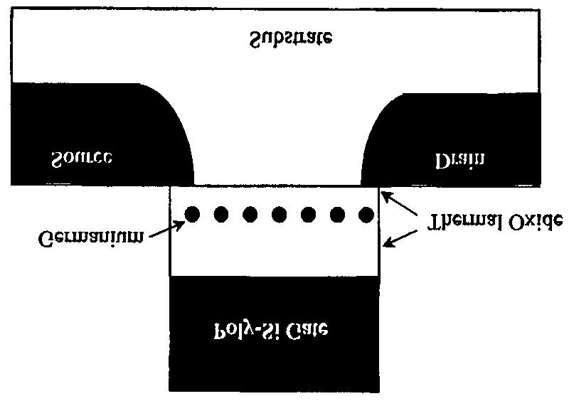
37 Geimplantation/Ge Segregation 37
38 Application u Major application fields: Memory Digital-data-storage Precision Measurement u Memory >> Logic We can use SE devices only in a memory cell, whereas keep using conventional CMOS technology in the peripheral circuitry. Memory cell technology has continuously changed, including the emergence of flash memory technology and ferroelectric-film memory technology. The way of storing information is rapidly changing from the old regime, relying on papers and other analog electronic means, to the digital regime in the multimedia era. New needs of storing information are different from the older specifications in bandwidth, storage capacity, power consumption. Fundamental difficulty in a logic functional unit since SE devices generally have poor current-drive capability. 38

39 Application-Data Storage System 39
40 Quantum Information- Qubit u Developing a quantum computer is a basic endeavor in science and technology. The advantage of Si-based quantum computer is Low cost Large scale integration u Contrast to classical bits, 0> or 1>, a quantum computer consists of Qubits, which could be represented by a superposition of 0> or 1>, i.e., α 0> +β 1> (where α 2 + β 2 =1) This huge parallelism makes it possible to solve some of the most difficult problems, such as integer factorization. 40

41 Quantum Computer Roadmap: development status After NTT Technical Review, June

42 Roadmap of Quantum Computer 42

43 Quantum Computer Roadmap: status of solid-state QC 43
44 Si-based Key Devices for QC Source Island Drain Si Figure 1. Schematic diagram for a single electron transistor and a coupled quantum dots. 利用單電子電晶體來檢測基本量子訊息 此地量子訊息是由耦合量子點建構而成 每一個量子點僅存在單一電子 因此耦合量子點的基態是自旋為零 (singlet), 利用電極與閘極電位使得單一量子點處在 0> 與 1> 的線性疊加狀態 0> 表示量子點只有單一電子 1> 表示量子點有兩個電子 此線性疊加態構成單位量子訊息 (quantum bit). 單電子電晶體的量子島耦合到耦合量子點 當電子從汲極穿隨進到量子島 將可以量測到量子點的狀態 整個元件佈局是一個非常難的技術 44


45 Accomplishments in NCU u Atomic-scale Ge QDsformed by thermal oxidation of SiGe-on-insulator. 20 min. Ge precipitation Buried Oxide 25 min. 45
46 Room-Temperature Characterization of Ge SETs Peak-to-valley current ratio (PVCR) of 1.92 is observed at room temperature 46 Clear offsets and plateaus are seen for gate voltages corresponding to the drain current valleys, while linear relations are obtained for gate voltages corresponding to the drain current peaks.
single-electron electron tunneling (SET)
") single-electron electron tunneling (SET) classical dots (SET islands): level spacing is NOT important; only the charging energy (=classical effect, many electrons on the island) quantum dots: : level spacing
single-electron electron tunneling (SET) classical dots (SET islands): level spacing is NOT important; only the charging energy (=classical effect, many electrons on the island) quantum dots: : level spacing
Chapter 3 Properties of Nanostructures
 Chapter 3 Properties of Nanostructures In Chapter 2, the reduction of the extent of a solid in one or more dimensions was shown to lead to a dramatic alteration of the overall behavior of the solids. Generally,
Building blocks for nanodevices
 Building blocks for nanodevices Two-dimensional electron gas (2DEG) Quantum wires and quantum point contacts Electron phase coherence Single-Electron tunneling devices - Coulomb blockage Quantum dots (introduction)
Lectures: Condensed Matter II 1 Electronic Transport in Quantum dots 2 Kondo effect: Intro/theory. 3 Kondo effect in nanostructures
 Lectures: Condensed Matter II 1 Electronic Transport in Quantum dots 2 Kondo effect: Intro/theory. 3 Kondo effect in nanostructures Luis Dias UT/ORNL Lectures: Condensed Matter II 1 Electronic Transport
Single-electron phenomena in semiconductors
 Semicond. Sci. Technol. 11 (1996) 255 284. Printed in the UK TOPICAL REVIEW Single-electron phenomena in semiconductors U Meirav and E B Foxman Braun Centre for Submicron Research, Weizmann Institute of
Fig. 8.1 : Schematic for single electron tunneling arrangement. For large system this charge is usually washed out by the thermal noise
 Part 2 : Nanostuctures Lecture 1 : Coulomb blockade and single electron tunneling Module 8 : Coulomb blockade and single electron tunneling Coulomb blockade and single electron tunneling A typical semiconductor
Electronic transport in low dimensional systems
 Electronic transport in low dimensional systems For example: 2D system l
Coulomb Blockade and Kondo Effect in Nanostructures
 Coulomb Blockade and Kondo Effect in Nanostructures Marcin M. Wysokioski 1,2 1 Institute of Physics Albert-Ludwigs-Universität Freiburg 2 Institute of Physics Jagiellonian University, Cracow, Poland 2.VI.2010
Nanoelectronics. Topics
 Nanoelectronics Topics Moore s Law Inorganic nanoelectronic devices Resonant tunneling Quantum dots Single electron transistors Motivation for molecular electronics The review article Overview of Nanoelectronic
From nanophysics research labs to cell phones. Dr. András Halbritter Department of Physics associate professor
 From nanophysics research labs to cell phones Dr. András Halbritter Department of Physics associate professor Curriculum Vitae Birth: 1976. High-school graduation: 1994. Master degree: 1999. PhD: 2003.
Single Electron Transistor (SET)
") Single Electron Transistor (SET) SET: e - e - dot A single electron transistor is similar to a normal transistor (below), except 1) the channel is replaced by a small dot. C g 2) the dot is separated from
Single Electron Transistor (SET) SET: e - e - dot A single electron transistor is similar to a normal transistor (below), except 1) the channel is replaced by a small dot. C g 2) the dot is separated from
Single Electron Transistor (SET)
") Single Electron Transistor (SET) e - e - dot C g V g A single electron transistor is similar to a normal transistor (below), except 1) the channel is replaced by a small dot. 2) the dot is separated from
Single Electron Transistor (SET) e - e - dot C g V g A single electron transistor is similar to a normal transistor (below), except 1) the channel is replaced by a small dot. 2) the dot is separated from
Formation of unintentional dots in small Si nanostructures
 Superlattices and Microstructures, Vol. 28, No. 5/6, 2000 doi:10.1006/spmi.2000.0942 Available online at http://www.idealibrary.com on Formation of unintentional dots in small Si nanostructures L. P. ROKHINSON,
GRAPHENE the first 2D crystal lattice
 GRAPHENE the first 2D crystal lattice dimensionality of carbon diamond, graphite GRAPHENE realized in 2004 (Novoselov, Science 306, 2004) carbon nanotubes fullerenes, buckyballs what s so special about
CHAPTER 2. Energy Bands and Carrier Concentration in Thermal Equilibrium
 CHAPTER 2 Energy Bands and Carrier Concentration in Thermal Equilibrium 光電特性 Ge 被 Si 取代, 因為 Si 有較低漏電流 Figure 2.1. Typical range of conductivities for insulators, semiconductors, and conductors. Figure
Classification of Solids
 Classification of Solids Classification by conductivity, which is related to the band structure: (Filled bands are shown dark; D(E) = Density of states) Class Electron Density Density of States D(E) Examples
Mesoscopic Nano-Electro-Mechanics of Shuttle Systems
 * Mesoscopic Nano-Electro-Mechanics of Shuttle Systems Robert Shekhter University of Gothenburg, Sweden Lecture1: Mechanically assisted single-electronics Lecture2: Quantum coherent nano-electro-mechanics
Single Electron Tunneling Examples
 Single Electron Tunneling Examples Danny Porath 2002 (Schönenberger et. al.) It has long been an axiom of mine that the little things are infinitely the most important Sir Arthur Conan Doyle Books and
Quantum Confinement in Graphene
 Quantum Confinement in Graphene from quasi-localization to chaotic billards MMM dominikus kölbl 13.10.08 1 / 27 Outline some facts about graphene quasibound states in graphene numerical calculation of
EN2912C: Future Directions in Computing Lecture 08: Overview of Near-Term Emerging Computing Technologies
 EN2912C: Future Directions in Computing Lecture 08: Overview of Near-Term Emerging Computing Technologies Prof. Sherief Reda Division of Engineering Brown University Fall 2008 1 Near-term emerging computing
Quasiadiabatic switching for metal-island quantum-dot cellular automata
 JOURNAL OF APPLIED PHYSICS VOLUME 85, NUMBER 5 1 MARCH 1999 Quasiadiabatic switching for metal-island quantum-dot cellular automata Géza Tóth and Craig S. Lent a) Department of Electrical Engineering,
Transport through Andreev Bound States in a Superconductor-Quantum Dot-Graphene System
 Transport through Andreev Bound States in a Superconductor-Quantum Dot-Graphene System Nadya Mason Travis Dirk, Yung-Fu Chen, Cesar Chialvo Taylor Hughes, Siddhartha Lal, Bruno Uchoa Paul Goldbart University
Quantum Phenomena & Nanotechnology (4B5)
") Quantum Phenomena & Nanotechnology (4B5) The 2-dimensional electron gas (2DEG), Resonant Tunneling diodes, Hot electron transistors Lecture 11 In this lecture, we are going to look at 2-dimensional electron
Quantum Phenomena & Nanotechnology (4B5) The 2-dimensional electron gas (2DEG), Resonant Tunneling diodes, Hot electron transistors Lecture 11 In this lecture, we are going to look at 2-dimensional electron
Chapter 6. Series-Parallel Circuits ISU EE. C.Y. Lee
 Chapter 6 Series-Parallel Circuits Objectives Identify series-parallel relationships Analyze series-parallel circuits Determine the loading effect of a voltmeter on a circuit Analyze a Wheatstone bridge
Quantum-dot cellular automata
 Quantum-dot cellular automata G. L. Snider, a) A. O. Orlov, I. Amlani, X. Zuo, G. H. Bernstein, C. S. Lent, J. L. Merz, and W. Porod Department of Electrical Engineering, University of Notre Dame, Notre
Large Storage Window in a-sinx/nc-si/a-sinx Sandwiched Structure
 2017 Asia-Pacific Engineering and Technology Conference (APETC 2017) ISBN: 978-1-60595-443-1 Large Storage Window in a-sinx/nc-si/a-sinx Sandwiched Structure Xiang Wang and Chao Song ABSTRACT The a-sin
Superconductivity at nanoscale
 Superconductivity at nanoscale Superconductivity is the result of the formation of a quantum condensate of paired electrons (Cooper pairs). In small particles, the allowed energy levels are quantized and
Charging and Kondo Effects in an Antidot in the Quantum Hall Regime
 Semiconductor Physics Group Cavendish Laboratory University of Cambridge Charging and Kondo Effects in an Antidot in the Quantum Hall Regime M. Kataoka C. J. B. Ford M. Y. Simmons D. A. Ritchie University
Charge spectrometry with a strongly coupled superconducting single-electron transistor
 PHYSICAL REVIEW B, VOLUME 64, 245116 Charge spectrometry with a strongly coupled superconducting single-electron transistor C. P. Heij, P. Hadley, and J. E. Mooij Applied Physics and Delft Institute of
Analysis of flip flop design using nanoelectronic single electron transistor
 Int. J. Nanoelectronics and Materials 10 (2017) 21-28 Analysis of flip flop design using nanoelectronic single electron transistor S.Rajasekaran*, G.Sundari Faculty of Electronics Engineering, Sathyabama
Zeeman splitting of single semiconductor impurities in resonant tunneling heterostructures
 Superlattices and Microstructures, Vol. 2, No. 4, 1996 Zeeman splitting of single semiconductor impurities in resonant tunneling heterostructures M. R. Deshpande, J. W. Sleight, M. A. Reed, R. G. Wheeler
Digital Electronics Part II - Circuits
 Digital Electronics Part - Circuits Dr.. J. Wassell Gates from Transistors ntroduction Logic circuits are non-linear, consequently we will introduce a graphical technique for analysing such circuits The
Lecture 20: Semiconductor Structures Kittel Ch 17, p , extra material in the class notes
 Lecture 20: Semiconductor Structures Kittel Ch 17, p 494-503, 507-511 + extra material in the class notes MOS Structure Layer Structure metal Oxide insulator Semiconductor Semiconductor Large-gap Semiconductor
Demonstration of a functional quantum-dot cellular automata cell
 Demonstration of a functional quantum-dot cellular automata cell Islamshah Amlani, a) Alexei O. Orlov, Gregory L. Snider, Craig S. Lent, and Gary H. Bernstein Department of Electrical Engineering, University
Tunneling transport. Courtesy Prof. S. Sawyer, RPI Also Davies Ch. 5
 unneling transport Courtesy Prof. S. Sawyer, RPI Also Davies Ch. 5 Electron transport properties l e : electronic mean free path l φ : phase coherence length λ F : Fermi wavelength ecture Outline Important
Emerging Research Devices: A Study of CNTFET and SET as a replacement for SiMOSFET
 1 Emerging Research Devices: A Study of CNTFET and SET as a replacement for SiMOSFET Mahmoud Lababidi, Krishna Natarajan, Guangyu Sun Abstract Since the development of the Silicon MOSFET, it has been the
Single-Electron Tunneling
 247 9 Single-Electron Tunneling The charge stored on a capacitor is not quantized: it consists of polarization charges generated by displacing the electron gas with respect to the positive lattice ions
ECE 340 Lecture 39 : MOS Capacitor II
 ECE 340 Lecture 39 : MOS Capacitor II Class Outline: Effects of Real Surfaces Threshold Voltage MOS Capacitance-Voltage Analysis Things you should know when you leave Key Questions What are the effects
Fabrication / Synthesis Techniques
 Quantum Dots Physical properties Fabrication / Synthesis Techniques Applications Handbook of Nanoscience, Engineering, and Technology Ch.13.3 L. Kouwenhoven and C. Marcus, Physics World, June 1998, p.35
Engineering 2000 Chapter 8 Semiconductors. ENG2000: R.I. Hornsey Semi: 1
 Engineering 2000 Chapter 8 Semiconductors ENG2000: R.I. Hornsey Semi: 1 Overview We need to know the electrical properties of Si To do this, we must also draw on some of the physical properties and we
Nanomaterials and their Optical Applications
 Nanomaterials and their Optical Applications Winter Semester 2013 Lecture 02 rachel.grange@uni-jena.de http://www.iap.uni-jena.de/multiphoton Lecture 2: outline 2 Introduction to Nanophotonics Theoretical
Multiple Gate CMOS and Beyond
 Multiple CMOS and Beyond Dept. of EECS, KAIST Yang-Kyu Choi Outline 1. Ultimate Scaling of MOSFETs - 3nm Nanowire FET - 8nm Non-Volatile Memory Device 2. Multiple Functions of MOSFETs 3. Summary 2 CMOS
半導體元件與物理. Semiconductor Devices and physics 許正興國立聯合大學電機工程學系 聯大電機系電子材料與元件應用實驗室
 半導體元件與物理 Semiconductor Devices and physics 許正興國立聯合大學電機工程學系 1. Crystal Structure of Solids 2. Quantum Theory of Solids 3. Semiconductor in Equilibrium and Carrier Transport phenomena 4. PN Junction and
Moores Law for DRAM. 2x increase in capacity every 18 months 2006: 4GB
 MEMORY Moores Law for DRAM 2x increase in capacity every 18 months 2006: 4GB Corollary to Moores Law Cost / chip ~ constant (packaging) Cost / bit = 2X reduction / 18 months Current (2008) ~ 1 micro-cent
Chapter 22 Lecture. Essential University Physics Richard Wolfson 2 nd Edition. Electric Potential 電位 Pearson Education, Inc.
 Chapter 22 Lecture Essential University Physics Richard Wolfson 2 nd Edition Electric Potential 電位 Slide 22-1 In this lecture you ll learn 簡介 The concept of electric potential difference 電位差 Including
Quantum Dot Structures Measuring Hamming Distance for Associative Memories
 Article Submitted to Superlattices and Microstructures Quantum Dot Structures Measuring Hamming Distance for Associative Memories TAKASHI MORIE, TOMOHIRO MATSUURA, SATOSHI MIYATA, TOSHIO YAMANAKA, MAKOTO
6.012 Electronic Devices and Circuits
 Page 1 of 12 YOUR NAME Department of Electrical Engineering and Computer Science Massachusetts Institute of Technology 6.012 Electronic Devices and Circuits FINAL EXAMINATION Open book. Notes: 1. Unless
Electrical Characterization with SPM Application Modules
 Electrical Characterization with SPM Application Modules Metrology, Characterization, Failure Analysis: Data Storage Magnetoresistive (MR) read-write heads Semiconductor Transistors Interconnect Ferroelectric
Section 12: Intro to Devices
 Section 12: Intro to Devices Extensive reading materials on reserve, including Robert F. Pierret, Semiconductor Device Fundamentals Bond Model of Electrons and Holes Si Si Si Si Si Si Si Si Si Silicon
Coulomb blockade and single electron tunnelling
 Coulomb blockade and single electron tunnelling Andrea Donarini Institute of theoretical physics, University of Regensburg Three terminal device Source System Drain Gate Variation of the electrostatic
0 0 = 1 0 = 0 1 = = 1 1 = 0 0 = 1
 0 0 = 1 0 = 0 1 = 0 1 1 = 1 1 = 0 0 = 1 : = {0, 1} : 3 (,, ) = + (,, ) = + + (, ) = + (,,, ) = ( + )( + ) + ( + )( + ) + = + = = + + = + = ( + ) + = + ( + ) () = () ( + ) = + + = ( + )( + ) + = = + 0
Herre van der Zant. interplay between molecular spin and electron transport (molecular spintronics) Gate
 Gate") transport through the single molecule magnet Mn12 Herre van der Zant H.B. Heersche, Z. de Groot (Delft) C. Romeike, M. Wegewijs (RWTH Aachen) D. Barreca, E. Tondello (Padova) L. Zobbi, A. Cornia (Modena)
transport through the single molecule magnet Mn12 Herre van der Zant H.B. Heersche, Z. de Groot (Delft) C. Romeike, M. Wegewijs (RWTH Aachen) D. Barreca, E. Tondello (Padova) L. Zobbi, A. Cornia (Modena)
Solid-State Spin Quantum Computers
 Solid-State Spin Quantum Computers 1 NV-Centers in Diamond P Donors in Silicon Kane s Computer (1998) P- doped silicon with metal gates Silicon host crystal + 31 P donor atoms + Addressing gates + J- coupling
Chapter 8: Coulomb blockade and Kondo physics
 Chater 8: Coulomb blockade and Kondo hysics 1) Chater 15 of Cuevas& Scheer. REFERENCES 2) Charge transort and single-electron effects in nanoscale systems, J.M. Thijssen and H.S.J. Van der Zant, Phys.
Quantum-Effect and Single-Electron Devices
 368 IEEE TRANSACTIONS ON NANOTECHNOLOGY, VOL. 2, NO. 4, DECEMBER 2003 Quantum-Effect and Single-Electron Devices Stephen M. Goodnick, Fellow, IEEE, and Jonathan Bird, Senior Member, IEEE Abstract In this
Semiconductor Physics and Devices Chapter 3.
 Introduction to the Quantum Theory of Solids We applied quantum mechanics and Schrödinger s equation to determine the behavior of electrons in a potential. Important findings Semiconductor Physics and
Semiconductor Nanowires: Motivation
 Semiconductor Nanowires: Motivation Patterning into sub 50 nm range is difficult with optical lithography. Self-organized growth of nanowires enables 2D confinement of carriers with large splitting of
Chapter 12: Electrical Properties. RA l
 Charge carriers and conduction: Chapter 12: Electrical Properties Charge carriers include all species capable of transporting electrical charge, including electrons, ions, and electron holes. The latter
arxiv:cond-mat/ v1 [cond-mat.mes-hall] 19 Aug 2005
![arxiv:cond-mat/ v1 [cond-mat.mes-hall] 19 Aug 2005](/thumbs/88/115668489.jpg "arxiv:cond-mat/ v1 [cond-mat.mes-hall] 19 Aug 2005") Coulomb-Blockade Oscillations in Semiconductor Nanostructures H. van Houten, C. W. J. Beenakker, and A. A. M. Staring Philips Research Laboratories, 5600 JA Eindhoven, The Netherlands arxiv:cond-mat/0508454v1
Coulomb-Blockade Oscillations in Semiconductor Nanostructures H. van Houten, C. W. J. Beenakker, and A. A. M. Staring Philips Research Laboratories, 5600 JA Eindhoven, The Netherlands arxiv:cond-mat/0508454v1
Spectroscopy at nanometer scale
 Spectroscopy at nanometer scale 1. Physics of the spectroscopies 2. Spectroscopies for the bulk materials 3. Experimental setups for the spectroscopies 4. Physics and Chemistry of nanomaterials Various
How a single defect can affect silicon nano-devices. Ted Thorbeck
 How a single defect can affect silicon nano-devices Ted Thorbeck tedt@nist.gov The Big Idea As MOS-FETs continue to shrink, single atomic scale defects are beginning to affect device performance Gate Source
Enhancement-mode quantum transistors for single electron spin
 Purdue University Purdue e-pubs Other Nanotechnology Publications Birck Nanotechnology Center 8-1-2006 Enhancement-mode quantum transistors for single electron spin G. M. Jones B. H. Hu C. H. Yang M. J.
Introduction to semiconductor nanostructures. Peter Kratzer Modern Concepts in Theoretical Physics: Part II Lecture Notes
 Introduction to semiconductor nanostructures Peter Kratzer Modern Concepts in Theoretical Physics: Part II Lecture Notes What is a semiconductor? The Fermi level (chemical potential of the electrons) falls
Lecture 8, April 12, 2017
 Lecture 8, April 12, 2017 This week (part 2): Semiconductor quantum dots for QIP Introduction to QDs Single spins for qubits Initialization Read-Out Single qubit gates Book on basics: Thomas Ihn, Semiconductor
Self-assembled SiGe single hole transistors
 Self-assembled SiGe single hole transistors G. Katsaros 1, P. Spathis 1, M. Stoffel 2, F. Fournel 3, M. Mongillo 1, V. Bouchiat 4, F. Lefloch 1, A. Rastelli 2, O. G. Schmidt 2 and S. De Franceschi 1 1
Electronic Quantum Transport in Mesoscopic Semiconductor Structures
 Thomas Ihn Electronic Quantum Transport in Mesoscopic Semiconductor Structures With 90 Illustrations, S in Full Color Springer Contents Part I Introduction to Electron Transport l Electrical conductance
Nanoimprint Lithography
 Nanoimprint Lithography Wei Wu Quantum Science Research Advanced Studies HP Labs, Hewlett-Packard Email: wei.wu@hp.com Outline Background Nanoimprint lithography Thermal based UV-based Applications based
New Model for Drain and Gate Current of Single-Electron Transistor at High Temperature
 World Journal of Nano Science and Engineering, 2012, 2, 171-175 http://dx.doi.org/10.4236/wjnse.2012.24022 Published Online ecember 2012 (http://www.scirp.org/journal/wjnse) New Model for rain and ate
During such a time interval, the MOS is said to be in "deep depletion" and the only charge present in the semiconductor is the depletion charge.
 Q1 (a) If we apply a positive (negative) voltage step to a p-type (n-type) MOS capacitor, which is sufficient to generate an inversion layer at equilibrium, there is a time interval, after the step, when
Semi-Conductors insulators semi-conductors N-type Semi-Conductors P-type Semi-Conductors
 Semi-Conductors In the metal materials considered earlier, the coupling of the atoms together to form the material decouples an electron from each atom setting it free to roam around inside the material.
FABRICATION AND CHARACTERIZATION OF SINGLE ELECTRON DEVICE AND STUDY OF ENERGY FILTERING IN SINGLE ELECTRON TRANSPORT LIANG-CHIEH MA
 FABRICATION AND CHARACTERIZATION OF SINGLE ELECTRON DEVICE AND STUDY OF ENERGY FILTERING IN SINGLE ELECTRON TRANSPORT by LIANG-CHIEH MA Presented to the Faculty of the Graduate School of The University
SUPPLEMENTARY INFORMATION
 Electrical control of single hole spins in nanowire quantum dots V. S. Pribiag, S. Nadj-Perge, S. M. Frolov, J. W. G. van den Berg, I. van Weperen., S. R. Plissard, E. P. A. M. Bakkers and L. P. Kouwenhoven
Commensurability-dependent transport of a Wigner crystal in a nanoconstriction
 NPCQS2012, OIST Commensurability-dependent transport of a Wigner crystal in a nanoconstriction David Rees, RIKEN, Japan Kimitoshi Kono (RIKEN) Paul Leiderer (University of Konstanz) Hiroo Totsuji (Okayama
A Tunable Kondo Effect in Quantum Dots
 A Tunable Kondo Effect in Quantum Dots Sara M. Cronenwett *#, Tjerk H. Oosterkamp *, and Leo P. Kouwenhoven * * Department of Applied Physics and DIMES, Delft University of Technology, PO Box 546, 26 GA
Supplementary Methods A. Sample fabrication
 Supplementary Methods A. Sample fabrication Supplementary Figure 1(a) shows the SEM photograph of a typical sample, with three suspended graphene resonators in an array. The cross-section schematic is
Choice of V t and Gate Doping Type
 Choice of V t and Gate Doping Type To make circuit design easier, it is routine to set V t at a small positive value, e.g., 0.4 V, so that, at V g = 0, the transistor does not have an inversion layer and
Quantum physics in quantum dots
 Quantum physics in quantum dots Klaus Ensslin Solid State Physics Zürich AFM nanolithography Multi-terminal tunneling Rings and dots Time-resolved charge detection Moore s Law Transistors per chip 10 9
Part 5: Quantum Effects in MOS Devices
 Quantum Effects Lead to Phenomena such as: Ultra Thin Oxides Observe: High Leakage Currents Through the Oxide - Tunneling Depletion in Poly-Si metal gate capacitance effect Thickness of Inversion Layer
Review of Optical Properties of Materials
 Review of Optical Properties of Materials Review of optics Absorption in semiconductors: qualitative discussion Derivation of Optical Absorption Coefficient in Direct Semiconductors Photons When dealing
Analytical Modeling of Threshold Voltage for a. Biaxial Strained-Si-MOSFET
 Contemporary Engineering Sciences, Vol. 4, 2011, no. 6, 249 258 Analytical Modeling of Threshold Voltage for a Biaxial Strained-Si-MOSFET Amit Chaudhry Faculty of University Institute of Engineering and
Single Electron transistors (SET) are one of the possible
 are one of the possible") Modulation of Coulomb Blockade Behavior of Room Temperature Operational Single Electron Transistors by Tunnel Junction P. Santosh Kumar Karre 1, Student Member, IEEE, Aditya Kapoor 2, Govind Mallick 3,
Modulation of Coulomb Blockade Behavior of Room Temperature Operational Single Electron Transistors by Tunnel Junction P. Santosh Kumar Karre 1, Student Member, IEEE, Aditya Kapoor 2, Govind Mallick 3,
Supercondcting Qubits
 Supercondcting Qubits Patricia Thrasher University of Washington, Seattle, Washington 98195 Superconducting qubits are electrical circuits based on the Josephson tunnel junctions and have the ability to
= lim(x + 1) lim x 1 x 1 (x 2 + 1) 2 (for the latter let y = x2 + 1) lim
 lim x 1 x 1 (x 2 + 1) 2 (for the latter let y = x2 + 1) lim") 1061 微乙 01-05 班期中考解答和評分標準 1. (10%) (x + 1)( (a) 求 x+1 9). x 1 x 1 tan (π(x )) (b) 求. x (x ) x (a) (5 points) Method without L Hospital rule: (x + 1)( x+1 9) = (x + 1) x+1 x 1 x 1 x 1 x 1 (x + 1) (for the
1061 微乙 01-05 班期中考解答和評分標準 1. (10%) (x + 1)( (a) 求 x+1 9). x 1 x 1 tan (π(x )) (b) 求. x (x ) x (a) (5 points) Method without L Hospital rule: (x + 1)( x+1 9) = (x + 1) x+1 x 1 x 1 x 1 x 1 (x + 1) (for the
Indium arsenide quantum wire trigate metal oxide semiconductor field effect transistor
 JOURNAL OF APPLIED PHYSICS 99, 054503 2006 Indium arsenide quantum wire trigate metal oxide semiconductor field effect transistor M. J. Gilbert a and D. K. Ferry Department of Electrical Engineering and
Single Electron Transistor
 Single Electron Transistor Sanjita Mandal Department of Electronics and Communication Engineering Shri Shankaracharya Institute of Professional Management and Technology, Raipur, Chhattisgarh, India Abstract-
Impact of disorder and topology in two dimensional systems at low carrier densities
 Impact of disorder and topology in two dimensional systems at low carrier densities A Thesis Submitted For the Degree of Doctor of Philosophy in the Faculty of Science by Mohammed Ali Aamir Department
UNIVERSITY OF CALIFORNIA College of Engineering Department of Electrical Engineering and Computer Sciences. Fall Exam 1
 UNIVERSITY OF CALIFORNIA College of Engineering Department of Electrical Engineering and Computer Sciences EECS 143 Fall 2008 Exam 1 Professor Ali Javey Answer Key Name: SID: 1337 Closed book. One sheet
Lecture 13: Barrier Penetration and Tunneling
 Lecture 13: Barrier Penetration and Tunneling nucleus x U(x) U(x) U 0 E A B C B A 0 L x 0 x Lecture 13, p 1 Today Tunneling of quantum particles Scanning Tunneling Microscope (STM) Nuclear Decay Solar
MSE 310/ECE 340: Electrical Properties of Materials Fall 2014 Department of Materials Science and Engineering Boise State University
 MSE 310/ECE 340: Electrical Properties of Materials Fall 2014 Department of Materials Science and Engineering Boise State University Practice Final Exam 1 Read the questions carefully Label all figures
No reason one cannot have double-well structures: With MBE growth, can control well thicknesses and spacings at atomic scale.
 The story so far: Can use semiconductor structures to confine free carriers electrons and holes. Can get away with writing Schroedinger-like equation for Bloch envelope function to understand, e.g., -confinement
Lecture 3: Heterostructures, Quasielectric Fields, and Quantum Structures
 Lecture 3: Heterostructures, Quasielectric Fields, and Quantum Structures MSE 6001, Semiconductor Materials Lectures Fall 2006 3 Semiconductor Heterostructures A semiconductor crystal made out of more
Supporting Online Material for
 www.sciencemag.org/cgi/content/full/320/5874/356/dc1 Supporting Online Material for Chaotic Dirac Billiard in Graphene Quantum Dots L. A. Ponomarenko, F. Schedin, M. I. Katsnelson, R. Yang, E. W. Hill,
Introduction to Molecular Electronics. Lecture 1: Basic concepts
 Introduction to Molecular Electronics Lecture 1: Basic concepts Conductive organic molecules Plastic can indeed, under certain circumstances, be made to behave very like a metal - a discovery for which
Stretching the Barriers An analysis of MOSFET Scaling. Presenters (in order) Zeinab Mousavi Stephanie Teich-McGoldrick Aseem Jain Jaspreet Wadhwa
 Zeinab Mousavi Stephanie Teich-McGoldrick Aseem Jain Jaspreet Wadhwa") Stretching the Barriers An analysis of MOSFET Scaling Presenters (in order) Zeinab Mousavi Stephanie Teich-McGoldrick Aseem Jain Jaspreet Wadhwa Why Small? Higher Current Lower Gate Capacitance Higher
Stretching the Barriers An analysis of MOSFET Scaling Presenters (in order) Zeinab Mousavi Stephanie Teich-McGoldrick Aseem Jain Jaspreet Wadhwa Why Small? Higher Current Lower Gate Capacitance Higher
Nanophysics: Main trends
 Nano-opto-electronics Nanophysics: Main trends Nanomechanics Main issues Light interaction with small structures Molecules Nanoparticles (semiconductor and metallic) Microparticles Photonic crystals Nanoplasmonics
Gate Carrier Injection and NC-Non- Volatile Memories
 Gate Carrier Injection and NC-Non- Volatile Memories Jean-Pierre Leburton Department of Electrical and Computer Engineering and Beckman Institute University of Illinois at Urbana-Champaign Urbana, IL 61801,
(a) (b) Supplementary Figure 1. (a) (b) (a) Supplementary Figure 2. (a) (b) (c) (d) (e)
 (b) Supplementary Figure 1. (a) (b) (a) Supplementary Figure 2. (a) (b) (c) (d) (e)") (a) (b) Supplementary Figure 1. (a) An AFM image of the device after the formation of the contact electrodes and the top gate dielectric Al 2 O 3. (b) A line scan performed along the white dashed line
(a) (b) Supplementary Figure 1. (a) An AFM image of the device after the formation of the contact electrodes and the top gate dielectric Al 2 O 3. (b) A line scan performed along the white dashed line
Cotunneling and Kondo effect in quantum dots. Part I/II
 & NSC Cotunneling and Kondo effect in quantum dots Part I/II Jens Paaske The Niels Bohr Institute & Nano-Science Center Bad Honnef, September, 2010 Dias 1 Lecture plan Part I 1. Basics of Coulomb blockade
Mat E 272 Lecture 25: Electrical properties of materials
 Mat E 272 Lecture 25: Electrical properties of materials December 6, 2001 Introduction: Calcium and copper are both metals; Ca has a valence of +2 (2 electrons per atom) while Cu has a valence of +1 (1
Metallic: 2n 1. +n 2. =3q Armchair structure always metallic = 2
 Properties of CNT d = 2.46 n 2 2 1 + n1n2 + n2 2π Metallic: 2n 1 +n 2 =3q Armchair structure always metallic a) Graphite Valence(π) and Conduction(π*) states touch at six points(fermi points) Carbon Nanotube: