半導體元件與物理. Semiconductor Devices and physics 許正興國立聯合大學電機工程學系 聯大電機系電子材料與元件應用實驗室
|
|
|
- Jessica McDonald
- 5 years ago
- Views:
Transcription
1 半導體元件與物理 Semiconductor Devices and physics 許正興國立聯合大學電機工程學系
2 1. Crystal Structure of Solids 2. Quantum Theory of Solids 3. Semiconductor in Equilibrium and Carrier Transport phenomena 4. PN Junction and Metal-Semiconductor 5. BJT 6. MOSFET 7. Optical Device
3 Part II 1. Allowed and Forbidden Energy Bands Formation of energy bands-> Kronig-Penney Model->k-space diagram 2. Electrical Conduction in Solids Energy band -> drift current -> electron effective mass->hole->metal, insulator and semiconductor 3. Density of States Function descriptive methods: Classical mechanics -> plants and satellites, Quantum mechanics -> electrons and high-frequency electromagnetic waves 4. Statistical Mechanics Fermi-Dirac Probability Function and Femi Energy
4 In this chapter, we will generalize these concepts to the electron in a crystal lattice. => one of goals is to determine the electrical properties of a semiconductor material, which we will then use to develop the current-voltage characteristics of semiconductor devices. to determine the properties of electrons in a crystal lattice, and to determine the statistical characteristics of the very large number of electrons in a crystal. Allowed and Forbidden Energy Bands Only discrete values of electron energy are allowed, The radial probability density for the electron was also determined. this function gives the probability of finding the electron at a particular distance from the nucleus and shows that the electron is not-localized at a given radius. apply quantum mechanics and Schrodinger s wave equation to the problem of an electron in a single crystal. we find that the electronic energy states occur in bands of allowed states that are separated by forbidden energy bands.
5 Formation of Energy Band Figure (a) shows the radial probability density function for the lowest electron energy state of the single, noninteracting hydrogen atom, figure (b) shows the same probability curves for two atoms that are in close proximity to each other. The wave functions of the two atom electrons overlap, which means that the two electrons will interact. this interaction or perturbation results in the discrete quantized energy level splitting into two discrete energy levels, schematically shown in figure (c). the splitting of the discrete state into two states is consistent with the Pauli exclusion principle.
6 A regular periodic arrangement of hydrogen-type atoms that are initially very far apart, and begin pushing the atoms together, the initial quantized energy level will split into a band of discrete energy levels. At the equilibrium interatomic distance (r 0 ), there is a band of allowed energies, but within the allowed band, the energies are at discrete levels. The Pauli exclusion principle states that the joining of atoms to form a system (crystal) does not alter the total number of quantum states regardless of size. Since no two electrons can have the same quantum number, the discrete energy must split into a band of energies in order that each electron can occupy a distinct quantum state.
7 Consider again a regular periodic arrangement of atoms, in which each atom now contains more than one electron. Suppose the atom in this imaginary crystal contains electrons up through n = 3 energy level. If the atoms are initially very far apart, the electrons in adjacent atoms will not interact and will occupy the discrete energy level. If these atoms are brought closer together, the outermost electrons in the n = 3 energy shell will begin to interact initially, so that this discrete energy level will split into a band of allowed energies. If the atoms continue to move closer together, the electrons in the n = 2 shell may begin to interact and will also split into a band of allowed energies. Finally, if the atoms become sufficiently close together, the innermost electrons in n = 1 level may interact, so that this energy level may also split into a band of allowed energies. If the equilibrium interatomic distance is r o, then w have bands of allowed energies that the electrons may occuply separated by bands of forbidden energies. Those definitions is the energy-band theory of single-crystal materials.

8 (a) Schematic representation of an isolated silicon atom. (b) the splitting of the 3s and 3p states of silicon into the allowed and forbidden energy bands. => As the interatomic distance decreases, the 3s and 3p states interact and overlap. At the equilibrium interatomic distance, the bands have again split, but now four quantum states per atom are in the lower band and four quantum states per atom are in the upper band. At absolute zero degrees, electrons are in the lowest energy state, so that all states in the lower band (the valence band) will be full and all state in the upper band (conduction band) will empty. the bandgap energy Eg between the top of the valence band and the bottom of the conduction band is the width of the forbidden energy band.
9 The Kronig-Penney Model The potential function of a single, noninteracting, one-electron atom is shown in Fig.a. Also indicated on the figure are the discrete energy levels allowed for the electron fig. b shows the same type of potential function for the case when several atoms are in close in a 1-D array. The potential functions of adjacent atoms overlap, and the net potential function for this case is shown in fig. c. => It is this potential function we would need to use in Schrodinger s wave equation to model a 1-D single-crystal material
10 The solution to Schrodinger s wave equation, for 1-D single-crystal lattice, is made more tractable by considering a simpler potential function. Figure is the 1-D Kronig-Penney model of the periodic potential function, which is used to represent a 1-D single-crystal lattice. we need to solve Schrodinger s wave equation in each region. As with previous quantum mechanical problems, the more interesting solution occurs for the case when E<V 0, which corresponds to a particle being bound within the crystal. => the electrons are contained in the potential wells, but we have the possibility of tunneling between wells. the Kronig-Penney model is an idealized periodic potential representing a 1-D single crystal, but the results will illustrate many of the important features of the quantum behavior of electrons in a periodic lattice.
11 The K-space Diagram From solve Schrodinger s wave function with differential the Kronig-Penney model defined region, we find the relation between the parameter k (constant of motion), total energy E and the potential barrier bv 0 P (sinαa/αa)+cosαa=coska ; but note that equation is not a solution of Schrodinger s wave function but gives the conditions for which Schrodinger s wave function will have a solution. To begin to understand the nature of the solution, initially consider the special case for which V 0 = 0. In the case P = 0, which corresponds to a free particle since there are no potential barrier. cosαa=coska or α=k Since the potential is equal to zero, the total energy E is equal to the kinetic energy, so that where p is the particle momentum
12 The constant of motion parameter k is related to the particle momentum for the free electron. The parameter k is also referred to as a wave number Relate the energy and momentum as Figure shows the parabolic relation of above equation between the energy E and momentum p for the free particle since the momentum and wave number are linearly related, figure is also the E versus k curve for the free particle. Consider he relation between E and k from above equation for the particle in the single-crystal lattice. As the parameter P increases, the particle becomes more tightly bound to the potential well or atom. we may define the left side of the above equation to be a function f(αa)
13 Figure a is a plot of the first term of above equation versus αa. Figure b shows a plot of the cosαa term and figure c is the sum of the two terms.
14 Figure shows this plot and shows the concept of allowed energy bands for the particle propagating in the crystal lattice. Since E has discontinuities, we also have the concept of forbidden energies for the particles in the crystal.
15 Consider again the right side of above equation, which is the function coska. where n is a positive integer Figure (left) shows how various segments of the curve can be displaced by 2π factor. Figure (right) shows the case in which the entire E versus k plot is contained within -π/a<k<π/a. This plot is referred to as a reduced k-space diagram, or reduced-zero representation.
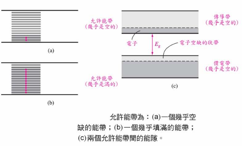
16 Electrical Conduction in Solids We are interested in determining the current-voltage characteristics of semiconductor devices. We will need to consider electrical conduction in solid as it relates to the band theory we have just developed. begin by considering the motion of electrons in the various allowed energy bands The energy band and the bond model All of the valence electrons are in the valence band. The upper energy band, the conduction band, is completely empty at T = 0 K. 2-D representation of the covalent bonding in a semiconductor at T = 0 K

17 As the temperature increases above 0 K, a few valence band electrons may gain enough thermal energy to break the covalent bond and jump into the conduction band. Figure a shows a 2-D representation of this bond-breaking effect and figure b, s simple line representation of the energy-band model, shows the same effect. The semiconductor is neutrally charged. This means that as the negatively charged electron breaks away from its covalent bonding position, a positively charged empty state is created in the original covalent bonding position in the valence band. as the temperature further increases, more covalent bands are broken, more electrons jump to the conduction band, and more positive empty states are created in the valence band.
18 We can also relate this bond breaking to the E versus k energy bands. Figure a shows the E versus k diagram of the conduction and valence bands at T = 0 K. The energy states in the valence band are completely full and the states in the conduction band are empty. => Figure b shows these same bands for T > 0 K, in which some electrons have gained enough energy to jump to the conduction band and have left empty states in the valence band.
19 Drift current Current is due to the net flow of charge. If we had a collection of positively charged ions with a volume density N (cm -3 ) and an average drift velocity v d (cm/s), then the drift current density would be If, instead of considering the average drift velocity, we considered the individual ion velocities, then we would write the drift current density as where v i is the velocity of the ith ion. Since electrons are charged particles, a net drift of electrons in the conduction band will give rise to a current. The electron distribution in the conduction band is an even function of k when no external force is applied. recall that k for a free electron is related to momentum so that, since there are as many electrons with a + k value as there are with a - k value, the net drift current density due to these electrons is zero certainly expected since there is no externally applied force. If a force is applied to particle and the particle moves, it must gain energy. if an external force is applied to the electrons in the conduction band, there are empty energy states into which the electrons can move; therefore, because of the external force, electrons can gain energy and a net momentum.
20 The electron distribution in the conduction band may look like as figure. The drift current density due to the motion of electron as

21 Electron effective mass The movement of an electron in a lattice will be different from that of an electron in free space. where internal force due to positively charged ions or protons and negatively charged electrons ; a is acceleration and m is the rest mass of the particle. since it is difficult to take into account all of the internal forces : where the acceleration a is now directly related to the external force, the parameter m* called the effective mass, takes into account the particle mass and also takes into account the effect of the internal force. => => take the second derivative The energy near the bottom of this energy band may be approximated by a parabola The energy Ec is the energy at the bottom of the band

22 Concept of Hole When a valence electron was elevated into the conduction band, a positively charged empty state was created. if a valence electron gains a small amount of thermal energy, it may hop into the empty state. the movement of a valence electron into the empty state is equivalent to the movement of the positively charge empty state itself.. Following figure show that the movement of valence electrons in the crystal alternately filling one empty state and creating a new empty state, a motion equivalent to a positive charge moving in the valence band. the crystal now has a second equally important charge carrier that can give rise to a current. this charge carrier is called a hole.
23 The drift current density due to electrons in the valence band, can be written as where the summation extends over all filled states. This summation is incovenient since it extends over a nearly full valence band and takes into account a very large number of states. If we consider a band that is totally full, all available states are occupies by electrons. The individual electrons can be thought of as moving with a velocity as given The band is symmetric in k and each state is occupied so that, for every electron with a velocity v, there is a corresponding electron with a velocity - v. Since the band is full, the distribution of electrons with respect to k cannot be changed with an externally applied force. the net drift current density generated from a completely full band, then, is zero, or the drift current density for an almost full band is where the v i in the summation is
24 The drift current density due to electrons in the valence band, can be written as where the summation extends over all filled states. This summation is incovenient since it extends over a nearly full valence band and takes into account a very large number of states. => If we consider a band that is totally full, all available states are occupies by electrons. The individual electrons can be thought of as moving with a velocity as given The band is symmetric in k and each state is occupied so that, for every electron with a velocity v, there is a corresponding electron with a velocity - v. Since the band is full, the distribution of electrons with respect to k cannot be charged with an externally applied force. the net drift current density generated from a completely full band, then, is zero, or
25 The drift current density for an almost full band as Above equation to placing a positively charged particle in the empty states and assuming all other states in the band are empty, or neutrally charged. The energy near the top of the allowed energy band Ev may again be approximated by a parabola so that we may write take the second derivative

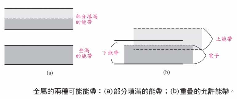
26 Metal, insulators, and semiconductors
27
28 Extension to three dimensions The basic concept of allowed and forbidden energy bands and the basic concept of effective mass have been developed in the last sections. And it also should be extend these concepts to 3-D and real crystals. we will qualitatively consider particular characteristics of the 3-D crystal in terms of the E versus k plots, bandgap energy and effective mass. The potential function to a 3-D crystal is that the distance between atoms varies as the direction through the crystal changes. Electrons traveling in different directions encounter different potential patterns and therefore different k-space boundaries. (in figure). The E versus k diagrams are in general a function of the k- space direction in a crystal.
29 Show different crystal directions.
30 Density of States Function Since current is due to the flow of charge, an important step in the process is to determine the number of electrons and holes in the semiconductor that will be available for conduction. The number of carriers that can contribute to the conduction process is a function of the number of available energy or quantum states since, by the Pauli exclusion principle, only one electron can occupy a given quantum state. discussed the splitting of energy levels into bands of allowed and forbidden energies, we indicated that the band of allowed energies was actually made up of discrete energy levels density of these allowed energy states as a function of energy in order to calculate the electron and hole concentrations.
31 Mathematical Derivation To determine the density of allowed quantum states as a function of energy, we need to consider an appropriate mathematical model. Electrons are allowed to move relatively freely in the conduction band of a semiconductor, but are confined to the crystal. As a first step, consider a free electron confined to a three-dimensional infinite potential well, where the potential well represent the crystal. => where the crystal is assumed to be a cube with length a Schrodinger s wave equation in 3-D can be solved using the separation of variables technique. => where n x, n y, n z are positive integers
32 We can schematically plot the allowed quantum states in k space. Figure shows a 2-D plot as a function of k x and k y. Each point represents an allowed quantum state corresponding to various integral values of n x and n y positive and negative values of k x, k y, k z have the same energy and represent the same energy state, but the density of quantum states will be determined by considering only the positive one-eighth of the spherical k space The distance between two quantum states in the k x direction, foe example, is given by => Generalizing this result to 3-D, the V k of a single quantum states is A differential volume in k space and is given by 4πk 2 dk, so the differential density of quantum states in k space can be written as
33 The first factor, 2, takes into account the two spin states allowed for each quantum state ; the next factor, (1/8), takes into account that we are considering only the quantum states for positive values of k x, k y, and k z. => Above equation gives the density of quantum states as a function of momentum, through the parameter k. for a free electron, the parameters E and k are related by => or The differential dk is Substituting above parameter to above equation, the number of energy states between E and E+dE is given by Since ħ = h / 2π Above equation gives the total number of quantum states between the energy E and E+dE in the crystal space volume of a 3 If we divide by the volume a 3, then the density of quantum states per unit volume of the crystal The density of quantum states is a function of energy E. as the energy of this free electron becomes small, the number of available quantum states decreases.
34 Extension to Semiconductors The parabolic relationship between energy and momentum of a free electron was given as E=p 2 /2m = ħ 2 h 2 /2m the E versus k curve near k=0 at the bottom of the conduction band can be approximated as a parabola so we may => the density of allowed electronic energy states in the conduction band as E E c The density of quantum states in the valence band can be obtained by using the same infinite potential well model since the hole is also confined in the semiconductor crystal and can be treated as a free particle. approximate the E versus k curve near k=0 The density of states function to apply to the valence band E E v The forbidden energy band, so g(e) = 0 for E v <E<E c,
35 Statistical Mechanics Fermi-Dirac Probability Function In determining the statistical behavior of particles, we must consider the laws that the particles obey. The Fermi-Dirac probability function, the particles are again indistinguishable, but now only one particle is permitted in each quantum state, electrons in a crystal obey this law. the particles are assumed to be noninteracting. We may write the most probable distribution function as Where E F is called the Fermi energy. The number density N(E) is the number of particles per unit volume per unit energy and the function g(e) is the number of quantum states per unit volume per unit energy. The function f F (E) is called the Fermi-Dirac distribution or probability function and gives the probability that a quantum states at the energy E will be occupied by an electron
36 The Distribution Function and the Fermi Energy To begin to understand the meaning of the distribution function and the Fermi energy, we can plot the distribution function versus energy. Let T=0 K and E <E F, exp[(e-e F )kt] exp(- ) = 0 f F (E<E F ) = 1 let T=0 K and E>E F => exp[(e-e F )kt] exp(+ ) + f F (E>E F ) = 0 The Fermi-Dirac distribution function for T = 0 K is plotted in Figure. => 1. for T = 0 K, the electrons are in their lowest possible energy states 2. probability of a quantum state being occupied is unity for E<E F and the probability of a state being occupied is aero for E>E F 3. All electrons have energies below the Fermi energy at T = 0 K

37 Left figure shows discrete energy levels of a particular as well as the number of available quantum at each energy (T = 0 K). the electrons will be in the lowest possible energy state the probability of a quantum state being occupied in energy levels E 1 through E 4 is unity ; probability of a quantum state being occupied in energy levels E 5 is zero. => for T >0 K, (as shows in right figure), several electrons from the E 4 have gained enough energy to jump to E 5 and from E 3 has jumped to E 4. As the temperature changes, the distribution of electrons versus energy changes. The density of quantum states g(e) is a continuous function of energy as middle figure. If we have N0 electrons in this system, then the distribution of these electrons among the quantum states at T = 0 K is shown by the dashed line. The electrons are in the lowest possible energy state so that all states below EF are filled and all states above E F are filled and all states above E F are empty. If g(e) and N 0 are known for this particular system, then the Fermi energy E F can be determined
38 The change in the electron distribution among energy levels for T > 0 K can be seen by plotting the Fermi-Dirac distribution function. If we let E = E F and T > 0 K, => the probability of a state being occupied at E = E F is 1/2. Fermi energy is independent of temperature.
39 We note that the probability of a state a distance de above E F being occupied is the same as the probability of a state a distance de below E F being empty the function f F (E) is symmetrical with the function 1-f F (E) about the Fermi energy, E F. => Consider the case when E-E F >>kt, where the exponential term in the denominator of above equation is much greater than unity neglect the 1 in the denominator, so that Fermi-Dirac distribution function becomes :
40
Semiconductor Physics and Devices Chapter 3.
 Introduction to the Quantum Theory of Solids We applied quantum mechanics and Schrödinger s equation to determine the behavior of electrons in a potential. Important findings Semiconductor Physics and
EE 346: Semiconductor Devices
 EE 346: Semiconductor Devices Lecture - 5 02/01/2017 Tewodros A. Zewde 1 The One-Electron Atom The potential function is due to the coulomb attraction between the proton and electron and is given by where
Introduction to Quantum Theory of Solids
 Lecture 5 Semiconductor physics III Introduction to Quantum Theory of Solids 1 Goals To determine the properties of electrons in a crystal lattice To determine the statistical characteristics of the very
Chapter 3: Introduction to the Quantum Theory of Solids
 Chapter 3: Introduction to the Quantum Theory of Solids Determine the properties of electrons in a crystal lattice. Determine the statistical characteristics of the very large number of electrons in a
Semiconductor Physics and Devices
 EE321 Fall 2015 September 28, 2015 Semiconductor Physics and Devices Weiwen Zou ( 邹卫文 ) Ph.D., Associate Prof. State Key Lab of advanced optical communication systems and networks, Dept. of Electronic
Communications with Optical Fibers
 Communications with Optical Fibers In digital communications, signals are generally sent as light pulses along an optical fiber. Information is first converted to an electrical signal in the form of pulses
The Semiconductor in Equilibrium
 Lecture 6 Semiconductor physics IV The Semiconductor in Equilibrium Equilibrium, or thermal equilibrium No external forces such as voltages, electric fields. Magnetic fields, or temperature gradients are
Bonding in solids The interaction of electrons in neighboring atoms of a solid serves the very important function of holding the crystal together.
 Bonding in solids The interaction of electrons in neighboring atoms of a solid serves the very important function of holding the crystal together. For example Nacl In the Nacl lattice, each Na atom is
EE 346: Semiconductor Devices
 EE 346: Semiconductor Devices Lecture - 6 02/06/2017 Tewodros A. Zewde 1 DENSTY OF STATES FUNCTON Since current is due to the flow of charge, an important step in the process is to determine the number
Calculating Band Structure
 Calculating Band Structure Nearly free electron Assume plane wave solution for electrons Weak potential V(x) Brillouin zone edge Tight binding method Electrons in local atomic states (bound states) Interatomic
Unit III Free Electron Theory Engineering Physics
 . Introduction The electron theory of metals aims to explain the structure and properties of solids through their electronic structure. The electron theory is applicable to all solids i.e., both metals
Ch. 2: Energy Bands And Charge Carriers In Semiconductors
 Ch. 2: Energy Bands And Charge Carriers In Semiconductors Discrete energy levels arise from balance of attraction force between electrons and nucleus and repulsion force between electrons each electron
DO PHYSICS ONLINE ELECTRIC CURRENT FROM IDEAS TO IMPLEMENTATION ATOMS TO TRANSISTORS ELECTRICAL PROPERTIES OF SOLIDS
 DO PHYSICS ONLINE FROM IDEAS TO IMPLEMENTATION 9.4.3 ATOMS TO TRANSISTORS ELECTRICAL PROPERTIES OF SOLIDS ELECTRIC CURRENT Different substances vary considerably in their electrical properties. It is a
Solid State Device Fundamentals
 Solid State Device Fundamentals ES 345 Lecture Course by Alexander M. Zaitsev alexander.zaitsev@csi.cuny.edu Tel: 718 982 2812 Oice 4101b 1 The ree electron model o metals The ree electron model o metals
ECE 442. Spring, Lecture -2
 ECE 442 Power Semiconductor Devices and Integrated circuits Spring, 2006 University of Illinois at Chicago Lecture -2 Semiconductor physics band structures and charge carriers 1. What are the types of
Minimal Update of Solid State Physics
 Minimal Update of Solid State Physics It is expected that participants are acquainted with basics of solid state physics. Therefore here we will refresh only those aspects, which are absolutely necessary
EE301 Electronics I , Fall
 EE301 Electronics I 2018-2019, Fall 1. Introduction to Microelectronics (1 Week/3 Hrs.) Introduction, Historical Background, Basic Consepts 2. Rewiev of Semiconductors (1 Week/3 Hrs.) Semiconductor materials
Resistance (R) Temperature (T)
 Temperature (T)") CHAPTER 1 Physical Properties of Elements and Semiconductors 1.1 Introduction Semiconductors constitute a large class of substances which have resistivities lying between those of insulators and conductors.
CHAPTER 1 Physical Properties of Elements and Semiconductors 1.1 Introduction Semiconductors constitute a large class of substances which have resistivities lying between those of insulators and conductors.
Charge Carriers in Semiconductor
 Charge Carriers in Semiconductor To understand PN junction s IV characteristics, it is important to understand charge carriers behavior in solids, how to modify carrier densities, and different mechanisms
Variation of Energy Bands with Alloy Composition E
 Variation of Energy Bands with Alloy Composition E 3.0 E.8.6 L 0.3eV Al x GaAs AlAs 1- xas 1.43eV.16eV X k.4 L. X.0 X 1.8 L 1.6 1.4 0 0. 0.4 0.6 X 0.8 1 1 Carriers in intrinsic Semiconductors Ec 4º 1º
Lecture 3: Electron statistics in a solid
 Lecture 3: Electron statistics in a solid Contents Density of states. DOS in a 3D uniform solid.................... 3.2 DOS for a 2D solid........................ 4.3 DOS for a D solid........................
Introduction to Engineering Materials ENGR2000. Dr.Coates
 Introduction to Engineering Materials ENGR2000 Chapter 18: Electrical Properties Dr.Coates 18.2 Ohm s Law V = IR where R is the resistance of the material, V is the voltage and I is the current. l R A
electronics fundamentals
 electronics fundamentals circuits, devices, and applications THOMAS L. FLOYD DAVID M. BUCHLA Lesson 1: Diodes and Applications Semiconductors Figure 1-1 The Bohr model of an atom showing electrons in orbits
The potential is minimum at the positive ion sites and maximum between the two ions.
 1. Bloch theorem: - A crystalline solid consists of a lattice, which is composed of a large number of ion cores at regular intervals, and the conduction electrons that can move freely through out the lattice.
Three Most Important Topics (MIT) Today
 Today") Three Most Important Topics (MIT) Today Electrons in periodic potential Energy gap nearly free electron Bloch Theorem Energy gap tight binding Chapter 1 1 Electrons in Periodic Potential We now know the
Three Most Important Topics (MIT) Today Electrons in periodic potential Energy gap nearly free electron Bloch Theorem Energy gap tight binding Chapter 1 1 Electrons in Periodic Potential We now know the
Modern Physics for Scientists and Engineers International Edition, 4th Edition
 Modern Physics for Scientists and Engineers International Edition, 4th Edition http://optics.hanyang.ac.kr/~shsong 1. THE BIRTH OF MODERN PHYSICS 2. SPECIAL THEORY OF RELATIVITY 3. THE EXPERIMENTAL BASIS
Chapter 4: Bonding in Solids and Electronic Properties. Free electron theory
 Chapter 4: Bonding in Solids and Electronic Properties Free electron theory Consider free electrons in a metal an electron gas. regards a metal as a box in which electrons are free to move. assumes nuclei
CLASS 1 & 2 REVISION ON SEMICONDUCTOR PHYSICS. Reference: Electronic Devices by Floyd
 CLASS 1 & 2 REVISION ON SEMICONDUCTOR PHYSICS Reference: Electronic Devices by Floyd 1 ELECTRONIC DEVICES Diodes, transistors and integrated circuits (IC) are typical devices in electronic circuits. All
Lecture 19: Building Atoms and Molecules
 Lecture 19: Building Atoms and Molecules +e r n = 3 n = 2 n = 1 +e +e r y even Lecture 19, p 1 Today Nuclear Magnetic Resonance Using RF photons to drive transitions between nuclear spin orientations in
Mat E 272 Lecture 25: Electrical properties of materials
 Mat E 272 Lecture 25: Electrical properties of materials December 6, 2001 Introduction: Calcium and copper are both metals; Ca has a valence of +2 (2 electrons per atom) while Cu has a valence of +1 (1
Lecture 2 Electrons and Holes in Semiconductors
 EE 471: Transport Phenomena in Solid State Devices Spring 2018 Lecture 2 Electrons and Holes in Semiconductors Bryan Ackland Department of Electrical and Computer Engineering Stevens Institute of Technology
Bohr s Model, Energy Bands, Electrons and Holes
 Dual Character of Material Particles Experimental physics before 1900 demonstrated that most of the physical phenomena can be explained by Newton's equation of motion of material particles or bodies and
Direct and Indirect Semiconductor
 Direct and Indirect Semiconductor Allowed values of energy can be plotted vs. the propagation constant, k. Since the periodicity of most lattices is different in various direction, the E-k diagram must
ELECTRONS IN A PERIODIC POTENTIAL AND ENERGY BANDS IN SOLIDS-2
 ELECTRONS IN A PERIODIC POTENTIAL AND ENERGY BANDS IN SOLIDS-2 ENERGY BANDS IN A SOLID : A FORMAL APPROACH SCHROEDINGER'S EQUATION FOR A PERIODIC POTENTIAL * Electrons motion in a crystal will now be considered
DO PHYSICS ONLINE STRUCTURE OF THE ATOM FROM IDEAS TO IMPLEMENTATION ATOMS TO TRANSISTORS STRUCTURE OF ATOMS AND SOLIDS
 DO PHYSIS ONLINE FROM IDEAS TO IMPLEMENTATION 9.4.3 ATOMS TO TRANSISTORS STRUTURE OF ATOMS AND SOLIDS STRUTURE OF THE ATOM In was not until the early 1930 s that scientists had fully developed a model
ECE440 Nanoelectronics. Lecture 07 Atomic Orbitals
 ECE44 Nanoelectronics Lecture 7 Atomic Orbitals Atoms and atomic orbitals It is instructive to compare the simple model of a spherically symmetrical potential for r R V ( r) for r R and the simplest hydrogen
CME 300 Properties of Materials. ANSWERS: Homework 9 November 26, As atoms approach each other in the solid state the quantized energy states:
 CME 300 Properties of Materials ANSWERS: Homework 9 November 26, 2011 As atoms approach each other in the solid state the quantized energy states: are split. This splitting is associated with the wave
Electronic Circuits for Mechatronics ELCT 609 Lecture 2: PN Junctions (1)
") Electronic Circuits for Mechatronics ELCT 609 Lecture 2: PN Junctions (1) Assistant Professor Office: C3.315 E-mail: eman.azab@guc.edu.eg 1 Electronic (Semiconductor) Devices P-N Junctions (Diodes): Physical
Electronic Circuits for Mechatronics ELCT 609 Lecture 2: PN Junctions (1) Assistant Professor Office: C3.315 E-mail: eman.azab@guc.edu.eg 1 Electronic (Semiconductor) Devices P-N Junctions (Diodes): Physical
3.024 Electrical, Optical, and Magnetic Properties of Materials Spring 2012 Recitation 8 Notes
 Overview 1. Electronic Band Diagram Review 2. Spin Review 3. Density of States 4. Fermi-Dirac Distribution 1. Electronic Band Diagram Review Considering 1D crystals with periodic potentials of the form:
Electronic Devices & Circuits
 Electronic Devices & Circuits For Electronics & Communication Engineering By www.thegateacademy.com Syllabus Syllabus for Electronic Devices Energy Bands in Intrinsic and Extrinsic Silicon, Carrier Transport,
Basic cell design. Si cell
 Basic cell design Si cell 1 Concepts needed to describe photovoltaic device 1. energy bands in semiconductors: from bonds to bands 2. free carriers: holes and electrons, doping 3. electron and hole current:
EE 446/646 Photovoltaic Devices I. Y. Baghzouz
 EE 446/646 Photovoltaic Devices I Y. Baghzouz What is Photovoltaics? First used in about 1890, the word has two parts: photo, derived from the Greek word for light, volt, relating to electricity pioneer
Chapter Two. Energy Bands and Effective Mass
 Chapter Two Energy Bands and Effective Mass Energy Bands Formation At Low Temperature At Room Temperature Valence Band Insulators Metals Effective Mass Energy-Momentum Diagrams Direct and Indirect Semiconduction
Lecture 19: Building Atoms and Molecules
 Lecture 19: Building Atoms and Molecules +e r n = 3 n = 2 n = 1 +e +e r ψ even Lecture 19, p 1 Today Nuclear Magnetic Resonance Using RF photons to drive transitions between nuclear spin orientations in
Solid State Device Fundamentals
 4. lectrons and Holes Solid State Device Fundamentals NS 45 Lecture Course by Alexander M. Zaitsev alexander.zaitsev@csi.cuny.edu Tel: 718 982 2812 4N101b 1 4. lectrons and Holes Free electrons and holes
ITT Technical Institute ET215 Devices I Unit 1
 ITT Technical Institute ET215 Devices I Unit 1 Chapter 1 Chapter 2, Sections 2.1-2.4 Chapter 1 Basic Concepts of Analog Circuits Recall ET115 & ET145 Ohms Law I = V/R If voltage across a resistor increases
Atoms? All matters on earth made of atoms (made up of elements or combination of elements).
.") Chapter 1 Atoms? All matters on earth made of atoms (made up of elements or combination of elements). Atomic Structure Atom is the smallest particle of an element that can exist in a stable or independent
Chapter 1 Atoms? All matters on earth made of atoms (made up of elements or combination of elements). Atomic Structure Atom is the smallest particle of an element that can exist in a stable or independent
Chapter 6 Free Electron Fermi Gas
 Chapter 6 Free Electron Fermi Gas Free electron model: The valence electrons of the constituent atoms become conduction electrons and move about freely through the volume of the metal. The simplest metals
ESE 372 / Spring 2013 / Lecture 5 Metal Oxide Semiconductor Field Effect Transistor
 Metal Oxide Semiconductor Field Effect Transistor V G V G 1 Metal Oxide Semiconductor Field Effect Transistor We will need to understand how this current flows through Si What is electric current? 2 Back
Lecture. Ref. Ihn Ch. 3, Yu&Cardona Ch. 2
 Lecture Review of quantum mechanics, statistical physics, and solid state Band structure of materials Semiconductor band structure Semiconductor nanostructures Ref. Ihn Ch. 3, Yu&Cardona Ch. 2 Reminder
EE143 Fall 2016 Microfabrication Technologies. Evolution of Devices
 EE143 Fall 2016 Microfabrication Technologies Prof. Ming C. Wu wu@eecs.berkeley.edu 511 Sutardja Dai Hall (SDH) 1-1 Evolution of Devices Yesterday s Transistor (1947) Today s Transistor (2006) 1-2 1 Why
Semiconductor Physics
 1 Semiconductor Physics 1.1 Introduction 2 1.2 The Band Theory of Solids 2 1.3 The Kronig Penney Model 3 1.4 The Bragg Model 8 1.5 Effective Mass 8 1.6 Number of States in a Band 10 1.7 Band Filling 12
EECS130 Integrated Circuit Devices
 EECS130 Integrated Circuit Devices Professor Ali Javey 8/30/2007 Semiconductor Fundamentals Lecture 2 Read: Chapters 1 and 2 Last Lecture: Energy Band Diagram Conduction band E c E g Band gap E v Valence
EE495/695 Introduction to Semiconductors I. Y. Baghzouz ECE Department UNLV
 EE495/695 Introduction to Semiconductors I Y. Baghzouz ECE Department UNLV Introduction Solar cells have always been aligned closely with other electronic devices. We will cover the basic aspects of semiconductor
Peak Electric Field. Junction breakdown occurs when the peak electric field in the PN junction reaches a critical value. For the N + P junction,
 Peak Electric Field Junction breakdown occurs when the peak electric field in the P junction reaches a critical value. For the + P junction, qa E ( x) ( xp x), s W dep 2 s ( bi Vr ) 2 s potential barrier
Electronic Devices And Circuits. Introduction
 Electronic Devices And Circuits Introduction An electronic device controls the movement of electrons. The study of electronic devices requires a basic understanding of the relationship between electrons
Chapter 1 Overview of Semiconductor Materials and Physics
 Chapter 1 Overview of Semiconductor Materials and Physics Professor Paul K. Chu Conductivity / Resistivity of Insulators, Semiconductors, and Conductors Semiconductor Elements Period II III IV V VI 2 B
Processing of Semiconducting Materials Prof. Pallab Banerji Department of Material Science Indian Institute of Technology, Kharagpur
 Processing of Semiconducting Materials Prof. Pallab Banerji Department of Material Science Indian Institute of Technology, Kharagpur Lecture - 4 Doping in Semiconductors Good morning. Let us start with
CHAPTER 2: ENERGY BANDS & CARRIER CONCENTRATION IN THERMAL EQUILIBRIUM. M.N.A. Halif & S.N. Sabki
 CHAPTER 2: ENERGY BANDS & CARRIER CONCENTRATION IN THERMAL EQUILIBRIUM OUTLINE 2.1 INTRODUCTION: 2.1.1 Semiconductor Materials 2.1.2 Basic Crystal Structure 2.1.3 Basic Crystal Growth technique 2.1.4 Valence
ECE 250 Electronic Devices 1. Electronic Device Modeling
 ECE 250 Electronic Devices 1 ECE 250 Electronic Device Modeling ECE 250 Electronic Devices 2 Introduction to Semiconductor Physics You should really take a semiconductor device physics course. We can only
Lecture 2. Unit Cells and Miller Indexes. Reading: (Cont d) Anderson 2 1.8,
 Anderson 2 1.8,") Lecture 2 Unit Cells and Miller Indexes Reading: (Cont d) Anderson 2 1.8, 2.1-2.7 Unit Cell Concept The crystal lattice consists of a periodic array of atoms. Unit Cell Concept A building block that can
Lecture 2 Unit Cells and Miller Indexes Reading: (Cont d) Anderson 2 1.8, 2.1-2.7 Unit Cell Concept The crystal lattice consists of a periodic array of atoms. Unit Cell Concept A building block that can
Nearly Free Electron Gas model - II
 Nearly Free Electron Gas model - II Contents 1 Lattice scattering 1 1.1 Bloch waves............................ 2 1.2 Band gap formation........................ 3 1.3 Electron group velocity and effective
A. F. J. Levi 1 EE539: Engineering Quantum Mechanics. Fall 2017.
 A. F. J. Levi 1 Engineering Quantum Mechanics. Fall 2017. TTh 9.00 a.m. 10.50 a.m., VHE 210. Web site: http://alevi.usc.edu Web site: http://classes.usc.edu/term-20173/classes/ee EE539: Abstract and Prerequisites
Lec. 8: Hydrogen Atom and Band Theory
 Solid State Electronics EC210 AAST Cairo Fall 2014 Lec. 8: Hydrogen Atom and Band Theory Fig 3.20 1 1 These PowerPoint color diagrams can only be used by instructors if the 3 rd Edition has been adopted
SEMICONDUCTOR PHYSICS
 SEMICONDUCTOR PHYSICS by Dibyendu Chowdhury Semiconductors The materials whose electrical conductivity lies between those of conductors and insulators, are known as semiconductors. Silicon Germanium Cadmium
Class 24: Density of States
 Class 24: Density of States The solution to the Schrödinger wave equation showed us that confinement leads to quantization. The smaller the region within which the electron is confined, the more widely
Quantum Conductance. John Carroll. March 22, 2009
 Quantum Conductance John Carroll March 22, 2009 Introduction The concept of conductance is used to explain the manner in which electrical current flows though a material. The original theory of conductance
PHYSICS 4750 Physics of Modern Materials Chapter 5: The Band Theory of Solids
 PHYSICS 4750 Physics of Modern Materials Chapter 5: The Band Theory of Solids 1. Introduction We have seen that when the electrons in two hydrogen atoms interact, their energy levels will split, i.e.,
Part II - Electronic Properties of Solids Lecture 12: The Electron Gas (Kittel Ch. 6) Physics 460 F 2006 Lect 12 1
 Physics 460 F 2006 Lect 12 1") Part II - Electronic Properties of Solids Lecture 12: The Electron Gas (Kittel Ch. 6) Physics 460 F 2006 Lect 12 1 Outline Overview - role of electrons in solids The starting point for understanding electrons
Part II - Electronic Properties of Solids Lecture 12: The Electron Gas (Kittel Ch. 6) Physics 460 F 2006 Lect 12 1 Outline Overview - role of electrons in solids The starting point for understanding electrons
Solid State Physics FREE ELECTRON MODEL. Lecture 14. A.H. Harker. Physics and Astronomy UCL
 Solid State Physics FREE ELECTRON MODEL Lecture 14 A.H. Harker Physics and Astronomy UCL 6 The Free Electron Model 6.1 Basic Assumptions In the free electron model, we assume that the valence electrons
ELEC311( 물리전자, Physical Electronics) Course Outlines:
 Course Outlines:") ELEC311( 물리전자, Physical Electronics) Course Outlines: by Professor Jung-Hee Lee Lecture notes are prepared with PPT and available before the class (http://abeek.knu.ac.kr). The topics in the notes are
ELEC311( 물리전자, Physical Electronics) Course Outlines: by Professor Jung-Hee Lee Lecture notes are prepared with PPT and available before the class (http://abeek.knu.ac.kr). The topics in the notes are
Crystal Properties. MS415 Lec. 2. High performance, high current. ZnO. GaN
 Crystal Properties Crystal Lattices: Periodic arrangement of atoms Repeated unit cells (solid-state) Stuffing atoms into unit cells Determine mechanical & electrical properties High performance, high current
Chapter 12: Semiconductors
 Chapter 12: Semiconductors Bardeen & Shottky January 30, 2017 Contents 1 Band Structure 4 2 Charge Carrier Density in Intrinsic Semiconductors. 6 3 Doping of Semiconductors 12 4 Carrier Densities in Doped
CHAPTER 2. Energy Bands and Carrier Concentration in Thermal Equilibrium
 CHAPTER 2 Energy Bands and Carrier Concentration in Thermal Equilibrium 光電特性 Ge 被 Si 取代, 因為 Si 有較低漏電流 Figure 2.1. Typical range of conductivities for insulators, semiconductors, and conductors. Figure
The general solution of Schrödinger equation in three dimensions (if V does not depend on time) are solutions of time-independent Schrödinger equation
 are solutions of time-independent Schrödinger equation") Lecture 27st Page 1 Lecture 27 L27.P1 Review Schrödinger equation The general solution of Schrödinger equation in three dimensions (if V does not depend on time) is where functions are solutions of time-independent
Lecture 27st Page 1 Lecture 27 L27.P1 Review Schrödinger equation The general solution of Schrödinger equation in three dimensions (if V does not depend on time) is where functions are solutions of time-independent
ELEMENTARY BAND THEORY
 ELEMENTARY BAND THEORY PHYSICIST Solid state band Valence band, VB Conduction band, CB Fermi energy, E F Bloch orbital, delocalized n-doping p-doping Band gap, E g Direct band gap Indirect band gap Phonon
Semiconductor Device Physics
 1 Semiconductor Device Physics Lecture 1 http://zitompul.wordpress.com 2 0 1 3 2 Semiconductor Device Physics Textbook: Semiconductor Device Fundamentals, Robert F. Pierret, International Edition, Addison
Introduction to Semiconductor Physics. Prof.P. Ravindran, Department of Physics, Central University of Tamil Nadu, India
 Introduction to Semiconductor Physics 1 Prof.P. Ravindran, Department of Physics, Central University of Tamil Nadu, India http://folk.uio.no/ravi/cmp2013 Review of Semiconductor Physics Semiconductor fundamentals
Book 2 Basic Semiconductor Devices for Electrical Engineers
 Book 2 Basic Semiconductor Devices for Electrical Engineers Professor C.R. Viswanathan Electrical and Computer Engineering Department University of California at Los Angeles Distinguished Professor Emeritus
Complete nomenclature for electron orbitals
 Complete nomenclature for electron orbitals Bohr s model worked but it lacked a satisfactory reason why. De Broglie suggested that all particles have a wave nature. u l=h/p Enter de Broglie again It was
Semiconductor physics I. The Crystal Structure of Solids
 Lecture 3 Semiconductor physics I The Crystal Structure of Solids 1 Semiconductor materials Types of solids Space lattices Atomic Bonding Imperfection and doping in SOLIDS 2 Semiconductor Semiconductors
Energy bands in solids. Some pictures are taken from Ashcroft and Mermin from Kittel from Mizutani and from several sources on the web.
 Energy bands in solids Some pictures are taken from Ashcroft and Mermin from Kittel from Mizutani and from several sources on the web. we are starting to remind p E = = mv 1 2 = k mv = 2 2 k 2m 2 Some
Lecture 1 - Electrons, Photons and Phonons. September 4, 2002
 6.720J/3.43J - Integrated Microelectronic Devices - Fall 2002 Lecture 1-1 Lecture 1 - Electrons, Photons and Phonons Contents: September 4, 2002 1. Electronic structure of semiconductors 2. Electron statistics
Electronic Structure of Surfaces
 Electronic Structure of Surfaces When solids made of an infinite number of atoms are formed, it is a common misconception to consider each atom individually. Rather, we must consider the structure of the
From Last Time Important new Quantum Mechanical Concepts. Atoms and Molecules. Today. Symmetry. Simple molecules.
 Today From Last Time Important new Quantum Mechanical Concepts Indistinguishability: Symmetries of the wavefunction: Symmetric and Antisymmetric Pauli exclusion principle: only one fermion per state Spin
ADVANCED UNDERGRADUATE LABORATORY EXPERIMENT 20. Semiconductor Resistance, Band Gap, and Hall Effect
 ADVANCED UNDERGRADUATE LABORATORY EXPERIMENT 20 Semiconductor Resistance, Band Gap, and Hall Effect Revised: November 1996 by David Bailey March 1990 by John Pitre & Taek-Soon Yoon Introduction Solid materials
ECE 335: Electronic Engineering Lecture 2: Semiconductors
 Faculty of Engineering ECE 335: Electronic Engineering Lecture 2: Semiconductors Agenda Intrinsic Semiconductors Extrinsic Semiconductors N-type P-type Carrier Transport Drift Diffusion Semiconductors
HALL EFFECT IN SEMICONDUCTORS
 Warsaw University of Technology Faculty of Physics Physics Laboratory I P Andrzej Kubiaczyk 30 HALL EFFECT IN SEMICONDUCTORS 1. ackground 1.1. Electron motion in electric and magnetic fields A particle
ENERGY BANDS AND GAPS IN SEMICONDUCTOR. Muhammad Hafeez Javed
 ENERGY BANDS AND GAPS IN SEMICONDUCTOR Muhammad Hafeez Javed www.rmhjaved.com rmhjaved@gmail.com Out Line Introduction Energy band Classification of materials Direct and indirect band gap of SC Classification
KATIHAL FİZİĞİ MNT-510
 KATIHAL FİZİĞİ MNT-510 YARIİLETKENLER Kaynaklar: Katıhal Fiziği, Prof. Dr. Mustafa Dikici, Seçkin Yayıncılık Katıhal Fiziği, Şakir Aydoğan, Nobel Yayıncılık, Physics for Computer Science Students: With
2) Atom manipulation. Xe / Ni(110) Model: Experiment:
 Atom manipulation. Xe / Ni(110) Model: Experiment:") 2) Atom manipulation D. Eigler & E. Schweizer, Nature 344, 524 (1990) Xe / Ni(110) Model: Experiment: G.Meyer, et al. Applied Physics A 68, 125 (1999) First the tip is approached close to the adsorbate
2) Atom manipulation D. Eigler & E. Schweizer, Nature 344, 524 (1990) Xe / Ni(110) Model: Experiment: G.Meyer, et al. Applied Physics A 68, 125 (1999) First the tip is approached close to the adsorbate
EE 3329 Electronic Devices Syllabus ( Extended Play )
") EE 3329 - Electronic Devices Syllabus EE 3329 Electronic Devices Syllabus ( Extended Play ) The University of Texas at El Paso The following concepts can be part of the syllabus for the Electronic Devices
EE 3329 - Electronic Devices Syllabus EE 3329 Electronic Devices Syllabus ( Extended Play ) The University of Texas at El Paso The following concepts can be part of the syllabus for the Electronic Devices
Basic Semiconductor Physics
 6 Basic Semiconductor Physics 6.1 Introduction With this chapter we start with the discussion of some important concepts from semiconductor physics, which are required to understand the operation of solar
Assumptions of classical free electron model
 Module 2 Electrical Conductivity in metals & Semiconductor 1) Drift Velocity :- The Velocity attain by an Electron in the Presence of applied electronic filed is Known as drift Velocity. 2) Mean free Path:-
Essentials of Quantum Physics
 Essentials of Quantum Physics References Direct energy conversion by S.W. Angrist, Ch 3. (out of print text book) Essential Quantum Physics by Peter Landshoff, Allen Metherell and Gareth Rees, 1997, Cambridge
Chapter 3 Properties of Nanostructures
 Chapter 3 Properties of Nanostructures In Chapter 2, the reduction of the extent of a solid in one or more dimensions was shown to lead to a dramatic alteration of the overall behavior of the solids. Generally,
Nearly Free Electron Gas model - I
 Nearly Free Electron Gas model - I Contents 1 Free electron gas model summary 1 2 Electron effective mass 3 2.1 FEG model for sodium...................... 4 3 Nearly free electron model 5 3.1 Primitive
Electrons in materials. (where are they, what is their energy)
") Electrons in materials (where are they, what is their energy) 1 Lone atoms A single atom has electrons in shells and sub shells. Each of these have a distinct energy level. The diagram shows an example
Electrons in materials (where are they, what is their energy) 1 Lone atoms A single atom has electrons in shells and sub shells. Each of these have a distinct energy level. The diagram shows an example
Final Exam Tuesday, May 8, 2012 Starting at 8:30 a.m., Hoyt Hall Duration: 2h 30m
 Final Exam Tuesday, May 8, 2012 Starting at 8:30 a.m., Hoyt Hall. ------------------- Duration: 2h 30m Chapter 39 Quantum Mechanics of Atoms Units of Chapter 39 39-1 Quantum-Mechanical View of Atoms 39-2
Derivation of the Boltzmann Distribution
 CLASSICAL CONCEPT REVIEW 7 Derivation of the Boltzmann Distribution Consider an isolated system, whose total energy is therefore constant, consisting of an ensemble of identical particles 1 that can exchange