Energy bands in solids. Some pictures are taken from Ashcroft and Mermin from Kittel from Mizutani and from several sources on the web.
|
|
|
- Charleen McDaniel
- 6 years ago
- Views:
Transcription
1 Energy bands in solids Some pictures are taken from Ashcroft and Mermin from Kittel from Mizutani and from several sources on the web.
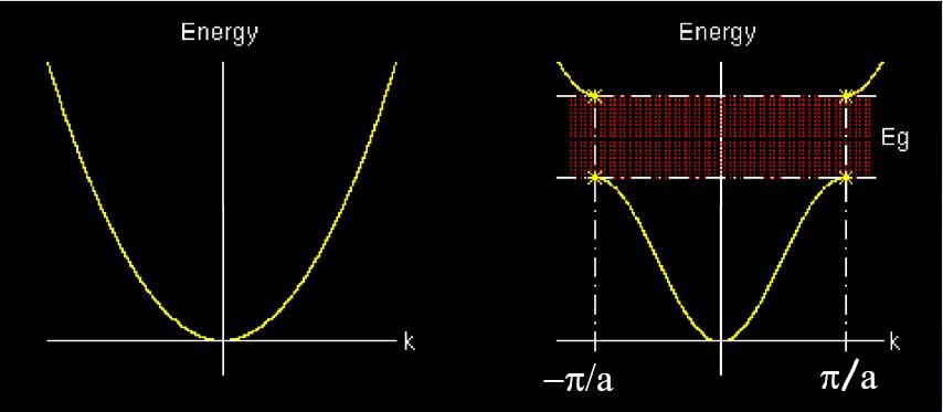
2 we are starting to remind p E = = mv 1 2 = k mv = 2 2 k 2m 2 Some pictures are taken from Ashcroft and Mermin from Kittel from Mizutani and from several sources on the web.
3
4
5
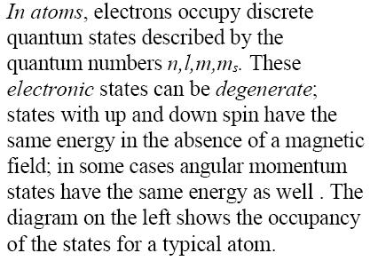
6 The letters s, p, d, f,..., are often used to signify the states with, l =0, 1, 2, 3,..., each preceded by the principal n=1, l = 0, m =0, s= 1/2 (1s) 2 n=2, l = 0, m =0, s= 1/2 (2s) 2 n=2, l = 1, m = 0, 1, s= 1/2 (2p) 6 n=3, l = 0, m =0, s= 1/2 (3s) 2 etc. Na 11 electrons with four different orbital energy levels 1s, 2s, 2p and 3s. (1s) 2 (2s) 2 (2p) 6 (3s) 1

7 from Alloul, Mizutani
8 the energy levels for the s electrons are split into quasi-continuously spaced energies when the interatomic distance is reduced to a few-tenths nm. The quasi-continuously spaced energy levels thus formed are called an energy band.
9 Apart from metallic bonding, there are three other bonding styles: ionic bonding, covalent bonding and van der Waals bonding (inert gases). Typical examples of ionic bonding are the crystals NaCl and K Cl. They are made up of positive and negative ions, which are alternately arranged at the lattice points of two interpenetrating simple cubic lattices. The electron configurations for both K + and Cl - ions in a KCl crystal are equally given as (1s) 2 (2s) 2 (2p) 6 (3s) 2 (3p) 6. See Mizutani for other examples!
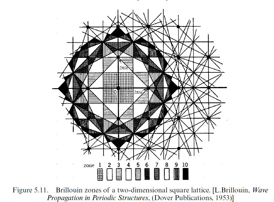
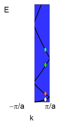
10 Free electron under the periodic boundary condition wigner-seitz cell in the reciprocal space

11 from Alloul from Kittel
12
13
14
15
16
17
18 1D L x 3D
19 Free electron in a box
20 from Alloul
 is called the Fermi energy and is a constant for each solid.")
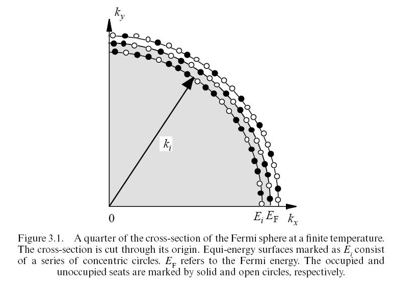
21 Construction of the Fermi sphere Pauli exclusion principle Fermi level the last occupied level = chemical potential = L k N F π π z z y y x x n L k n L k n L k = = = π π π ,, 0 ± ± n = The value of the Fermi level at absolute zero ( C) is called the Fermi energy and is a constant for each solid. Mizutani
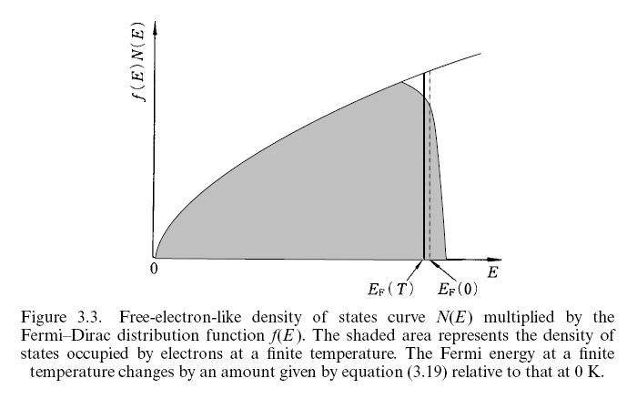
22 density of states dn = N( E) de
23 a mole of sodium metal weighs g with its density 0.97 g/cm 3. Since it is a monovalent metal, N 0 (# electrons) is equal to the Avogadro number N A. N A = and V= nm 3 results in a Fermi radius k F =9.1 nm -1 for sodium metal. N= number of valence electrons per atom (e/a) bcc strucure, a= nm, the volume per atom Na monovalent: 1 electron/atom- E F = 3.2 ev Fermi temperature: E F = K B T F if E F = 5eV T F = K
24
25 Mizutani
26 Mizutani
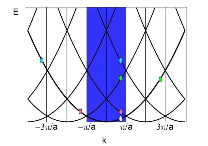
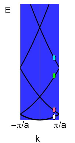
27 1D free electrons a G G k E k E na L L x x l i π = + = = + = ψ ψ 2 ) ( ) ( ) ( ) ( 1,0 2,... 1,0 2,... ) ( ± ± = ± ± = n e x ika ψ ) 2 ( 2 ) ( a k m k E π + = l : empty lattice model
28
29
30
")
31 (NEF model)
32
33 T 0 K
34
35
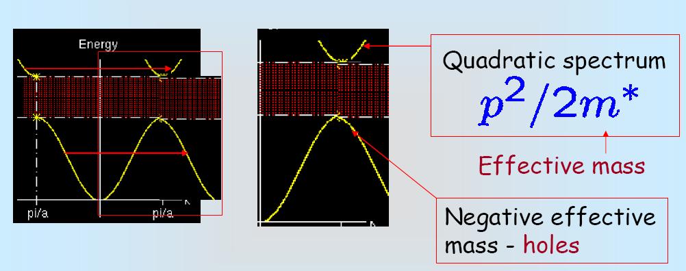
36
37 NFE approxination Kittel
38 (perturbation theory) Kittel
39 Mizutani
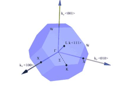
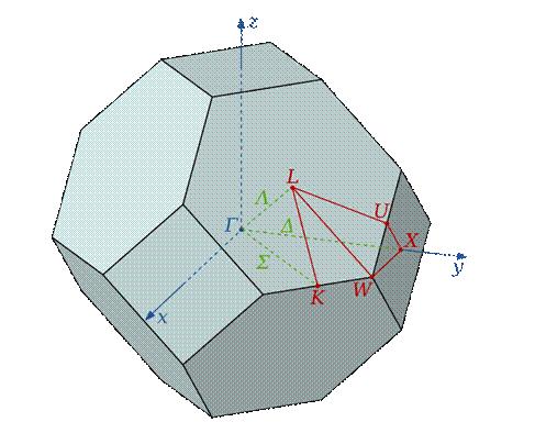
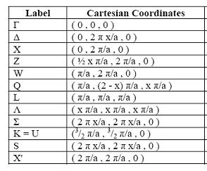
40 Fermi surface Brillouin zone interaction Mizutani
41 Mizutani The Fermi surface begins to be distorted from a sphere before making contacts with the Brillouin zone planes.

42
43 Mizutani

44 see Mizutani for detalis
45 Effective mass E = 2 k 2m 2 de dk = 2 k m p m = k E F = m * a
46
47
48 2 E 2 k < 0 m * < 0 2 E 2 k > 0 m * > 0
49
50 Interpretation The electron is subject to internal forces from the lattice (ions and core electrons) AND external forces such as electric fields In a crystal lattice, the net force may be opposite the external force, however: F ext =-qe - F int =-de p /dx E p (x)
51 Interpretation electron acceleration is not equal to F ext /m e, but rather a = (F ext + F int )/m e = F ext /m * The dispersion relation E(K) compensates for the internal forces due to the crystal and allows us to use classical concepts for the electron as long as its mass is taken as m * F ext =-qe - F int =-de p /dx E p (x)
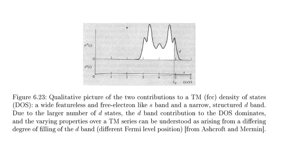
52 Examples of Energy Bands in Solids What we can find out: see Mizutani for more details

53 Metal is a solid with a Fermi surface!
54
55
56
57
58
59
, BZ is half-filled #electrons in the reciprocal unit cell (2")
60 from the UvA-VU Master Course: Advanced Solid State Physics by Anne de Visser (University of Amsterdam), BZ is half-filled #electrons in the reciprocal unit cell (2 atoms/u.c.)


61 Na metal is known to be almost a free-electron-like metal. Mizutani empty lattice calculation

62 Van Hove anomaly
63

64 from the UvA-VU Master Course: Advanced Solid State Physics by Anne de Visser (University of Amsterdam),
65
66 Mizutani
67
68
69
70
71 In the case of copper, the bands near the Fermi level are derived from the 4s and 3d atomic levels. The so-called 4s and 3d bands accommodate a total of 12 electrons, while the number of available electrons is 11. Therefore the Fermi level must cross these bands. Consequently copper is metallic.
72 As another unique feature of the electronic structure of noble metals, the parabolic E k relation is intervened by the less dispersive E k curves due to 3d electrons centered at about a few ev below the Fermi level. This means that the 4s and 4p free-electron-like states are hybridized with the 3d states to form a composite band. In spite of strong hybridization, ten 3d electrons per atom are distributed in a rather narrow energy range. The Fermi surface of a noble metal should occupy only 50% by volume of the first Brillouin zone of the fcc lattice.

73 Polyvalent Metals see Mizutani The two outermost 4s electrons per atom contribute to the formation of the valence band of Ca metal. Since the number of electrons per atom, e/a, is equal to 2.0, it is just high enough to fill the first Brillouin zone.
74 The simplest example of a polyvalent metal is aluminum with 3 electrons/atom and having a 3s 2 3p electronic configuration for the valence electrons. Because of the partial filling of the 3s 2 3p 6 bands, aluminum is a metal. Aluminum crystallizes in the FCC structure The energy bands for aluminum are very free electron-like. from Mizutani
75
76
77
78
79 semimetal electronic band structure intermediate between metals and semiconductors small Fermi surfaces of both electrons and holes Mizutani a very small overlap between the bottom of the conduction band and the top of the valence band
80 It can be seen that the two bands slightly overlap each other so that electrons and holes coexist at the Fermi level.
, Si, Ge and")


81 The elements C (diamond), Si, Ge and Sn( α) belong to the group IVB elements in the periodic table and all of them are covalently bonded.
82 Two interpenetrating fcc lattices and, hence, the structure is fcc but with two atoms in each unit cell. In Si, two 3s and two 3p electrons per atom are hybridized to form directionally-bonded states and the Brillouin zone is completely filled with eight electrons per unit cell. Hence, no Fermi surface exists. Kittel
83
84 Energy gaps of typical semiconductors are as follows: 5.3 ev for C (diamond), 1.1 ev for Si, 0.7 ev for Ge, 2.8 ev for SiC, 4.6 ev for BN and 1.4 ev for GaAs.
85


86 Is there a Fermi energy of intrinsic Semiconductors? ε F If is defined as the energy separating the highest occupied from the lowest unoccupied level, then it is not uniquely specified in a solid with an energy gap, since any energy in the gap meets this test. People nevertheless speak of the Fermi energy on an intrinsic semiconductor. What they mean is the chemical potential, which is well defined at any non-zero temperature. As T 0, the chemical potential of a solid with an energy gap approaches the energy of the middle of the gap and one sometimes finds it asserted that this is the Fermi energy. With either the correct of colloquial definition, ε does not have a solution in a n( k) = εf solid with a gap, which therefore has no Fermi surface!
87 extrinsic semiconductors Si semiconducting properties depend significantly on whether pentavalent or trivalent impurities are added. Pentavalent atoms like P, As and Sb from group VB of the periodic table will have one more valence electron than is required for the covalent bonding. Donor As 5+ Mizutani
88 Acceptor B 3+ trivalent atoms like B, Al, Ga and In from group IIIB in the periodic table possess one electron less than the number required for covalent bonding. Hence, an electron from one of the adjacent Si atoms will enter the orbit about the trivalent impurity atom. This causes the trivalent atom to be negatively charged and the host Si atoms to lose an electron in this process.
89
90 Mizutani
91 Mizutani
92 Culity, Graham Introduction to magnetic materials Wiley 2009.
93
 E B = µ B B The small")

94 Pauli Paramagnetism W. Pauli Nobel Price 1945 Spin - Magnetization for small fields B (T=0) E B = µ B B The small size of the paramagnetic susceptibility of most metals was a puzzle until Pauli pointed out that is was a consequence of the fact that electrons obey Fermi Dirac rather than classical statistics. M n = g( EF ) E E = 2µ 2 ( n n ) g( E ) µ B = B B µ = B F B
95 Pauli paramagnetism is a weak effect compared to paramagnetism in insulators (in insulators one electron at each ion contributes, in metals only the electrons at the Fermi level contribute). Magnetic Spin - Susceptibility ( ) F B P F B F F F B P E N B M H M T k N E N E g E g B M H M ) ( µ µ = µ = = χ = = µ = µ µ = = χ (Pauli Paramagnetism)
96 Culity, Graham Introduction to magnetic materials Wiley 2009.
97 - Copper is diamagnetic, since (a) its Fermi energy is close to the band edge [i.e.g(e F ) is small] and thus χ p is relatively small, and (b) copper has ten d-electrons (i.e. Z 10) orbiting on a fairly large radius, which results in a large χ dia. - Also in bivalent metals (e.g. Be) g(e F ) is small they are diamagnetic - In semiconductors, the valence bands are filled, i.e. g(e F ) = 0 semiconductors have no paramagnetic susceptibility and are diamagnetic
98 Direct Exchange between delocalized Electrons Itinerant ferromagnetism Spontaneously Split bands: e.g. Fe M = 2.2μ B /f.u. is non integer... this is strong evidence for band ferromagnetism Mean field Model: all spins feel the same exchange field λm produced by all their neighbors, this exchange field can magnetize the electron gas spontaneously via the Pauli Paramagnetism, if λ and χ P are large enough. Quantitative estimation: what is the condition that the system as a whole can save energy by becoming ferromagnetic?
 δe M = 1 1.")
99 M ( n ) = µ n B moving D e (E F )δe/2 electrons from spin down to spin up band kinetic energy change: ( ) 2 E exchange energy change: 1 2 K. E. = De ( EF ) δe M = ) 2 2 E µ B ( λm ') dm ' = µ λm = µ ( n EP λµ n
100 see Mizutani

.")
101 U n total energy change: µ n 0 E µ = 2 B λ D e = E ( E K. E. F ) δe + E P. E. = 1 2 D e ( E F ) 2 ( δe) ( 1 UD ( E )) there is an energy gain by spontaneous magnetization, if UD ( E e F )... Coulomb Effects must be strong and density of states at the Fermi energy must be large in order to get sponatneous ferromagnetism in metals. 1 e F Stoner Criterion Edmund C. Stoner ( )
102 from Mizutani
103
104 kittel
105 kittel
106
107 Figure shows the calculated valence band structure for the spin-up and spin-down electrons in ferromagnetic Ni metal. It can be seen that the spin-up band is shifted to higher binding energies relative to the spin-down band because of the exchange energy. The Fermi level is determined by fitting a total of 10 electrons per atom into the hybridized 3d and 4s bands. It is clear that the 3d spin-up band is fully filled by electrons while the Fermi level falls in the middle of the 3d spin-down band, leaving holes in this sub-band. The number of holes per atom is calculated to be ~ 0.6. This is obviously proportional to the magnetization of pure Ni metal and is consistent with the observed non-integer value
108 Ni 1-x Cu x average electron concentration (Cu:[Ar] 3d 10 4s 1 ) Ni 1-x Zn x (Zn: [Ar] 3d 10 4s 2 ) M=0, for x = 0.6 X= 0.3 the Ni 3d spin-down band possessing 0.6 holes per atom will be filled when x=0.6 Hence, the Ni 3d spin-down band will be filled at x= 0.3 Mizutani
109 Mizutani
110
111 from Mizutani
112
113 see Mizutani
Ch. 2: Energy Bands And Charge Carriers In Semiconductors
 Ch. 2: Energy Bands And Charge Carriers In Semiconductors Discrete energy levels arise from balance of attraction force between electrons and nucleus and repulsion force between electrons each electron
ELEMENTARY BAND THEORY
 ELEMENTARY BAND THEORY PHYSICIST Solid state band Valence band, VB Conduction band, CB Fermi energy, E F Bloch orbital, delocalized n-doping p-doping Band gap, E g Direct band gap Indirect band gap Phonon
Three Most Important Topics (MIT) Today
 Today") Three Most Important Topics (MIT) Today Electrons in periodic potential Energy gap nearly free electron Bloch Theorem Energy gap tight binding Chapter 1 1 Electrons in Periodic Potential We now know the
Three Most Important Topics (MIT) Today Electrons in periodic potential Energy gap nearly free electron Bloch Theorem Energy gap tight binding Chapter 1 1 Electrons in Periodic Potential We now know the
Density of states for electrons and holes. Distribution function. Conduction and valence bands
 Intrinsic Semiconductors In the field of semiconductors electrons and holes are usually referred to as free carriers, or simply carriers, because it is these particles which are responsible for carrying
Nearly Free Electron Gas model - I
 Nearly Free Electron Gas model - I Contents 1 Free electron gas model summary 1 2 Electron effective mass 3 2.1 FEG model for sodium...................... 4 3 Nearly free electron model 5 3.1 Primitive
ELEC311( 물리전자, Physical Electronics) Course Outlines:
 Course Outlines:") ELEC311( 물리전자, Physical Electronics) Course Outlines: by Professor Jung-Hee Lee Lecture notes are prepared with PPT and available before the class (http://abeek.knu.ac.kr). The topics in the notes are
ELEC311( 물리전자, Physical Electronics) Course Outlines: by Professor Jung-Hee Lee Lecture notes are prepared with PPT and available before the class (http://abeek.knu.ac.kr). The topics in the notes are
Bonding in solids The interaction of electrons in neighboring atoms of a solid serves the very important function of holding the crystal together.
 Bonding in solids The interaction of electrons in neighboring atoms of a solid serves the very important function of holding the crystal together. For example Nacl In the Nacl lattice, each Na atom is
Semiconductor Physics and Devices Chapter 3.
 Introduction to the Quantum Theory of Solids We applied quantum mechanics and Schrödinger s equation to determine the behavior of electrons in a potential. Important findings Semiconductor Physics and
Calculating Band Structure
 Calculating Band Structure Nearly free electron Assume plane wave solution for electrons Weak potential V(x) Brillouin zone edge Tight binding method Electrons in local atomic states (bound states) Interatomic
Chapter 3. Crystal Binding
 Chapter 3. Crystal Binding Energy of a crystal and crystal binding Cohesive energy of Molecular crystals Ionic crystals Metallic crystals Elasticity What causes matter to exist in three different forms?
Variation of Energy Bands with Alloy Composition E
 Variation of Energy Bands with Alloy Composition E 3.0 E.8.6 L 0.3eV Al x GaAs AlAs 1- xas 1.43eV.16eV X k.4 L. X.0 X 1.8 L 1.6 1.4 0 0. 0.4 0.6 X 0.8 1 1 Carriers in intrinsic Semiconductors Ec 4º 1º
Crystal Properties. MS415 Lec. 2. High performance, high current. ZnO. GaN
 Crystal Properties Crystal Lattices: Periodic arrangement of atoms Repeated unit cells (solid-state) Stuffing atoms into unit cells Determine mechanical & electrical properties High performance, high current
1.4 Crystal structure
 1.4 Crystal structure (a) crystalline vs. (b) amorphous configurations short and long range order only short range order Abbildungen: S. Hunklinger, Festkörperphysik, Oldenbourg Verlag represenatives of
Ionic Bonding. Example: Atomic Radius: Na (r = 0.192nm) Cl (r = 0.099nm) Ionic Radius : Na (r = 0.095nm) Cl (r = 0.181nm)
 Cl (r = 0.099nm) Ionic Radius : Na (r = 0.095nm) Cl (r = 0.181nm)") Ionic Bonding Ion: an atom or molecule that gains or loses electrons (acquires an electrical charge). Atoms form cations (+charge), when they lose electrons, or anions (- charge), when they gain electrons.
Ionic Bonding Ion: an atom or molecule that gains or loses electrons (acquires an electrical charge). Atoms form cations (+charge), when they lose electrons, or anions (- charge), when they gain electrons.
Introduction to Engineering Materials ENGR2000. Dr.Coates
 Introduction to Engineering Materials ENGR2000 Chapter 18: Electrical Properties Dr.Coates 18.2 Ohm s Law V = IR where R is the resistance of the material, V is the voltage and I is the current. l R A
The Oxford Solid State Basics
 The Oxford Solid State Basics Steven H. Simon University of Oxford OXFORD UNIVERSITY PRESS Contents 1 About Condensed Matter Physics 1 1.1 What Is Condensed Matter Physics 1 1.2 Why Do We Study Condensed
EECS130 Integrated Circuit Devices
 EECS130 Integrated Circuit Devices Professor Ali Javey 8/30/2007 Semiconductor Fundamentals Lecture 2 Read: Chapters 1 and 2 Last Lecture: Energy Band Diagram Conduction band E c E g Band gap E v Valence
Nearly Free Electron Gas model - II
 Nearly Free Electron Gas model - II Contents 1 Lattice scattering 1 1.1 Bloch waves............................ 2 1.2 Band gap formation........................ 3 1.3 Electron group velocity and effective
Paramagnetism and Diamagnetism. Paramagnets (How do paramagnets differ fundamentally from ferromagnets?)
") Paramagnetism and Diamagnetism Paramagnets (How do paramagnets differ fundamentally from ferromagnets?) The study of paramagnetism allows us to investigate the atomic magnetic moments of atoms almost in
Paramagnetism and Diamagnetism Paramagnets (How do paramagnets differ fundamentally from ferromagnets?) The study of paramagnetism allows us to investigate the atomic magnetic moments of atoms almost in
Lecture 3: Electron statistics in a solid
 Lecture 3: Electron statistics in a solid Contents Density of states. DOS in a 3D uniform solid.................... 3.2 DOS for a 2D solid........................ 4.3 DOS for a D solid........................
2 B B D (E) Paramagnetic Susceptibility. m s probability. A) Bound Electrons in Atoms
 Paramagnetic Susceptibility. m s probability. A) Bound Electrons in Atoms") Paramagnetic Susceptibility A) Bound Electrons in Atoms m s probability B +½ p ½e x Curie Law: 1/T s=½ + B ½ p + ½e +x With increasing temperature T the alignment of the magnetic moments in a B field is
Paramagnetic Susceptibility A) Bound Electrons in Atoms m s probability B +½ p ½e x Curie Law: 1/T s=½ + B ½ p + ½e +x With increasing temperature T the alignment of the magnetic moments in a B field is
Atomic Structure. Atomic weight = m protons + m neutrons Atomic number (Z) = # of protons Isotope corresponds to # of neutrons
 = # of protons Isotope corresponds to # of neutrons") Atomic Structure Neutrons: neutral Protons: positive charge (1.6x10 19 C, 1.67x10 27 kg) Electrons: negative charge (1.6x10 19 C, 9.11x10 31 kg) Atomic weight = m protons + m neutrons Atomic number (Z)
Atomic Structure Neutrons: neutral Protons: positive charge (1.6x10 19 C, 1.67x10 27 kg) Electrons: negative charge (1.6x10 19 C, 9.11x10 31 kg) Atomic weight = m protons + m neutrons Atomic number (Z)
Chapter Outline Understanding of interatomic bonding is the first step towards understanding/explaining materials properties Review of Atomic
 Chapter Outline Understanding of interatomic bonding is the first step towards understanding/explaining materials properties Review of Atomic Structure: Electrons, Protons, Neutrons, Quantum mechanics
Chapter 4: Bonding in Solids and Electronic Properties. Free electron theory
 Chapter 4: Bonding in Solids and Electronic Properties Free electron theory Consider free electrons in a metal an electron gas. regards a metal as a box in which electrons are free to move. assumes nuclei
The Semiconductor in Equilibrium
 Lecture 6 Semiconductor physics IV The Semiconductor in Equilibrium Equilibrium, or thermal equilibrium No external forces such as voltages, electric fields. Magnetic fields, or temperature gradients are
Introductory Nanotechnology ~ Basic Condensed Matter Physics ~
 Introductory Nanotechnology ~ Basic Condensed Matter Physics ~ Atsufumi Hirohata Department of Electronics Go into Nano-Scale Lateral Size [m] 10-3 10-6 Micron-scale Sub-Micron-scale Nano-scale Human hair
CLASS 12th. Semiconductors
 CLASS 12th Semiconductors 01. Distinction Between Metals, Insulators and Semi-Conductors Metals are good conductors of electricity, insulators do not conduct electricity, while the semiconductors have
Chapter Outline Understanding of interatomic bonding is the first step towards understanding/explaining materials properties Review of Atomic
 Chapter Outline Understanding of interatomic bonding is the first step towards understanding/explaining materials properties Review of Atomic Structure: Electrons, Protons, Neutrons, Quantum mechanics
763333A SOLDID STATE PHYSICS Exercise 1 Spring 2013
 763333A SOLDID STATE PHYSICS Exercise 1 Spring 2013 1. Fcc as a Bravais lattice Show that the fcc structure is a Bravais lattice. For this choose appropriate a 1, a 2 and a 3 so that the expression r =
DEVELOPMENT OF THE PERIODIC TABLE
 DEVELOPMENT OF THE PERIODIC TABLE Prior to the 1700s, relatively few element were known, and consisted mostly of metals used for coinage, jewelry and weapons. From early 1700s to mid-1800s, chemists discovered
Atoms? All matters on earth made of atoms (made up of elements or combination of elements).
.") Chapter 1 Atoms? All matters on earth made of atoms (made up of elements or combination of elements). Atomic Structure Atom is the smallest particle of an element that can exist in a stable or independent
Chapter 1 Atoms? All matters on earth made of atoms (made up of elements or combination of elements). Atomic Structure Atom is the smallest particle of an element that can exist in a stable or independent
Electrons, Holes, and Defect ionization
 Electrons, Holes, and Defect ionization The process of forming intrinsic electron-hole pairs is excitation a cross the band gap ( formation energy ). intrinsic electronic reaction : null e + h When electrons
MTLE-6120: Advanced Electronic Properties of Materials. Intrinsic and extrinsic semiconductors. Reading: Kasap:
 MTLE-6120: Advanced Electronic Properties of Materials 1 Intrinsic and extrinsic semiconductors Reading: Kasap: 5.1-5.6 Band structure and conduction 2 Metals: partially filled band(s) i.e. bands cross
Atoms, Molecules and Solids (selected topics)
") Atoms, Molecules and Solids (selected topics) Part I: Electronic configurations and transitions Transitions between atomic states (Hydrogen atom) Transition probabilities are different depending on the
Atoms, Molecules and Solids (selected topics) Part I: Electronic configurations and transitions Transitions between atomic states (Hydrogen atom) Transition probabilities are different depending on the
Quantum Condensed Matter Physics Lecture 4
 Quantum Condensed Matter Physics Lecture 4 David Ritchie QCMP Lent/Easter 2019 http://www.sp.phy.cam.ac.uk/drp2/home 4.1 Quantum Condensed Matter Physics 1. Classical and Semi-classical models for electrons
Electromagnetism II. Instructor: Andrei Sirenko Spring 2013 Thursdays 1 pm 4 pm. Spring 2013, NJIT 1
 Electromagnetism II Instructor: Andrei Sirenko sirenko@njit.edu Spring 013 Thursdays 1 pm 4 pm Spring 013, NJIT 1 PROBLEMS for CH. 6 http://web.njit.edu/~sirenko/phys433/phys433eandm013.htm Can obtain
Chapter 3: Introduction to the Quantum Theory of Solids
 Chapter 3: Introduction to the Quantum Theory of Solids Determine the properties of electrons in a crystal lattice. Determine the statistical characteristics of the very large number of electrons in a
Lecture 18: Semiconductors - continued (Kittel Ch. 8)
") Lecture 18: Semiconductors - continued (Kittel Ch. 8) + a - Donors and acceptors J U,e e J q,e Transport of charge and energy h E J q,e J U,h Physics 460 F 2006 Lect 18 1 Outline More on concentrations
Lecture 18: Semiconductors - continued (Kittel Ch. 8) + a - Donors and acceptors J U,e e J q,e Transport of charge and energy h E J q,e J U,h Physics 460 F 2006 Lect 18 1 Outline More on concentrations
EE143 Fall 2016 Microfabrication Technologies. Evolution of Devices
 EE143 Fall 2016 Microfabrication Technologies Prof. Ming C. Wu wu@eecs.berkeley.edu 511 Sutardja Dai Hall (SDH) 1-1 Evolution of Devices Yesterday s Transistor (1947) Today s Transistor (2006) 1-2 1 Why
Semiconductor physics I. The Crystal Structure of Solids
 Lecture 3 Semiconductor physics I The Crystal Structure of Solids 1 Semiconductor materials Types of solids Space lattices Atomic Bonding Imperfection and doping in SOLIDS 2 Semiconductor Semiconductors
Section 10 Metals: Electron Dynamics and Fermi Surfaces
 Electron dynamics Section 10 Metals: Electron Dynamics and Fermi Surfaces The next important subject we address is electron dynamics in metals. Our consideration will be based on a semiclassical model.
Basic cell design. Si cell
 Basic cell design Si cell 1 Concepts needed to describe photovoltaic device 1. energy bands in semiconductors: from bonds to bands 2. free carriers: holes and electrons, doping 3. electron and hole current:
Solid State Physics. Lecture 10 Band Theory. Professor Stephen Sweeney
 Solid State Physics Lecture 10 Band Theory Professor Stephen Sweeney Advanced Technology Institute and Department of Physics University of Surrey, Guildford, GU2 7XH, UK s.sweeney@surrey.ac.uk Recap from
CHAPTER 2: ENERGY BANDS & CARRIER CONCENTRATION IN THERMAL EQUILIBRIUM. M.N.A. Halif & S.N. Sabki
 CHAPTER 2: ENERGY BANDS & CARRIER CONCENTRATION IN THERMAL EQUILIBRIUM OUTLINE 2.1 INTRODUCTION: 2.1.1 Semiconductor Materials 2.1.2 Basic Crystal Structure 2.1.3 Basic Crystal Growth technique 2.1.4 Valence
Minimal Update of Solid State Physics
 Minimal Update of Solid State Physics It is expected that participants are acquainted with basics of solid state physics. Therefore here we will refresh only those aspects, which are absolutely necessary
Direct and Indirect Semiconductor
 Direct and Indirect Semiconductor Allowed values of energy can be plotted vs. the propagation constant, k. Since the periodicity of most lattices is different in various direction, the E-k diagram must
Professor K. Section 8 Electron Configuration Periodic Table
 Professor K Section 8 Electron Configuration Periodic Table Schrödinger Cannot be solved for multielectron atoms We must assume the orbitals are all hydrogen-like Differences In the H atom, all subshells
3.23 Electrical, Optical, and Magnetic Properties of Materials
 MIT OpenCourseWare http://ocw.mit.edu 3.23 Electrical, Optical, and Magnetic Properties of Materials Fall 2007 For information about citing these materials or our Terms of Use, visit: http://ocw.mit.edu/terms.
Electrons in a periodic potential
 Chapter 3 Electrons in a periodic potential 3.1 Bloch s theorem. We consider in this chapter electrons under the influence of a static, periodic potential V (x), i.e. such that it fulfills V (x) = V (x
 lectures accompanying the book: Solid State Physics: An Introduction, by Philip ofmann (2nd edition 2015, ISBN-10: 3527412824, ISBN-13: 978-3527412822, Wiley-VC Berlin. www.philiphofmann.net 1 Bonds between
First-Principles Calculation of Exchange Interactions
 Chapter 2 First-Principles Calculation of Exchange Interactions Before introducing the first-principles methods for the calculation of exchange interactions in magnetic systems we will briefly review two
Chemistry 121: Topic 4 - Chemical Bonding Topic 4: Chemical Bonding
 Topic 4: Chemical Bonding 4.0 Ionic and covalent bonds; Properties of covalent and ionic compounds 4.1 Lewis structures, the octet rule. 4.2 Molecular geometry: the VSEPR approach. Molecular polarity.
Lecture 2: Bonding in solids
 Lecture 2: Bonding in solids Electronegativity Van Arkel-Ketalaar Triangles Atomic and ionic radii Band theory of solids Molecules vs. solids Band structures Analysis of chemical bonds in Reciprocal space
Solids. properties & structure
 Solids properties & structure Determining Crystal Structure crystalline solids have a very regular geometric arrangement of their particles the arrangement of the particles and distances between them is
PHY380 Solid State Physics
 PHY380 Solid State Physics Professor Maurice Skolnick, Dr Dmitry Krizhanovskii and Professor David Lidzey Syllabus 1. The distinction between insulators, semiconductors and metals. The periodic table.
EECS143 Microfabrication Technology
 EECS143 Microfabrication Technology Professor Ali Javey Introduction to Materials Lecture 1 Evolution of Devices Yesterday s Transistor (1947) Today s Transistor (2006) Why Semiconductors? Conductors e.g
1 Review of semiconductor materials and physics
 Part One Devices 1 Review of semiconductor materials and physics 1.1 Executive summary Semiconductor devices are fabricated using specific materials that offer the desired physical properties. There are
I. Introduction II. Solid State Physics Detection of Light Bernhard Brandl 1
 Detection of Light I. Introduction II. Solid State Physics 4-2-2015 Detection of Light Bernhard Brandl 1 4-2-2015 Detection of Light Bernhard Brandl 2 Blabla Recommended 4-2-2015 Detection of Light Bernhard
半導體元件與物理. Semiconductor Devices and physics 許正興國立聯合大學電機工程學系 聯大電機系電子材料與元件應用實驗室
 半導體元件與物理 Semiconductor Devices and physics 許正興國立聯合大學電機工程學系 1. Crystal Structure of Solids 2. Quantum Theory of Solids 3. Semiconductor in Equilibrium and Carrier Transport phenomena 4. PN Junction and
Atomic Structure & Interatomic Bonding
 Atomic Structure & Interatomic Bonding Chapter Outline Review of Atomic Structure Atomic Bonding Atomic Structure Atoms are the smallest structural units of all solids, liquids & gases. Atom: The smallest
SOLID STATE PHYSICS. Second Edition. John Wiley & Sons. J. R. Hook H. E. Hall. Department of Physics, University of Manchester
 SOLID STATE PHYSICS Second Edition J. R. Hook H. E. Hall Department of Physics, University of Manchester John Wiley & Sons CHICHESTER NEW YORK BRISBANE TORONTO SINGAPORE Contents Flow diagram Inside front
Electronic structure of correlated electron systems. Lecture 2
 Electronic structure of correlated electron systems Lecture 2 Band Structure approach vs atomic Band structure Delocalized Bloch states Fill up states with electrons starting from the lowest energy No
(FIRST) IONIZATION ENERGY
 IONIZATION ENERGY") 181 (FIRST) IONIZATION ENERGY - The amount of energy required to remove a single electron from the outer shell of an atom. - Relates to reactivity for metals. The easier it is to remove an electron, the
181 (FIRST) IONIZATION ENERGY - The amount of energy required to remove a single electron from the outer shell of an atom. - Relates to reactivity for metals. The easier it is to remove an electron, the
The broad topic of physical metallurgy provides a basis that links the structure of materials with their properties, focusing primarily on metals.
 Physical Metallurgy The broad topic of physical metallurgy provides a basis that links the structure of materials with their properties, focusing primarily on metals. Crystal Binding In our discussions
Lecture 2 Electrons and Holes in Semiconductors
 EE 471: Transport Phenomena in Solid State Devices Spring 2018 Lecture 2 Electrons and Holes in Semiconductors Bryan Ackland Department of Electrical and Computer Engineering Stevens Institute of Technology
CHAPTER 3. Crystallography
 CHAPTER 3 Crystallography Atomic Structure Atoms are made of Protons: mass 1.00728 amu, +1 positive charge Neutrons: mass of 1.00867 amu, neutral Electrons: mass of 0.00055 amu, -1 negative charge (1 amu
Physics of Condensed Matter I
 Physics of Condensed Matter I 1100-4INZ`PC Solid State 1 Faculty of Physics UW Jacek.Szczytko@fuw.edu.pl Chemical bonding and molecules Born Oppenheimer approximation Max Born (1882-1970) Jacob R. Oppenheimer
Lecture. Ref. Ihn Ch. 3, Yu&Cardona Ch. 2
 Lecture Review of quantum mechanics, statistical physics, and solid state Band structure of materials Semiconductor band structure Semiconductor nanostructures Ref. Ihn Ch. 3, Yu&Cardona Ch. 2 Reminder
Chapter 1 Overview of Semiconductor Materials and Physics
 Chapter 1 Overview of Semiconductor Materials and Physics Professor Paul K. Chu Conductivity / Resistivity of Insulators, Semiconductors, and Conductors Semiconductor Elements Period II III IV V VI 2 B
PH575 Spring Lecture #13 Free electron theory: Sutton Ch. 7 pp 132 -> 144; Kittel Ch. 6. 3/2 " # % & D( E) = V E 1/2. 2π 2.
 = V E 1/2. 2π 2.") PH575 Spring 2014 Lecture #13 Free electron theory: Sutton Ch. 7 pp 132 -> 144; Kittel Ch. 6. E( k) = 2 k 2 D( E) = V 2π 2 " # $ 2 3/2 % & ' E 1/2 Assumption: electrons metal do not interact with each
PH575 Spring 2014 Lecture #13 Free electron theory: Sutton Ch. 7 pp 132 -> 144; Kittel Ch. 6. E( k) = 2 k 2 D( E) = V 2π 2 " # $ 2 3/2 % & ' E 1/2 Assumption: electrons metal do not interact with each
EE 346: Semiconductor Devices
 EE 346: Semiconductor Devices Lecture - 6 02/06/2017 Tewodros A. Zewde 1 DENSTY OF STATES FUNCTON Since current is due to the flow of charge, an important step in the process is to determine the number
- Some properties of elements can be related to their positions on the periodic table.
 179 PERIODIC TRENDS - Some properties of elements can be related to their positions on the periodic table. ATOMIC RADIUS - The distance between the nucleus of the atoms and the outermost shell of the electron
Lecture 7: Extrinsic semiconductors - Fermi level
 Lecture 7: Extrinsic semiconductors - Fermi level Contents 1 Dopant materials 1 2 E F in extrinsic semiconductors 5 3 Temperature dependence of carrier concentration 6 3.1 Low temperature regime (T < T
EXTRINSIC SEMICONDUCTOR
 EXTRINSIC SEMICONDUCTOR In an extrinsic semiconducting material, the charge carriers originate from impurity atoms added to the original material is called impurity [or] extrinsic semiconductor. This Semiconductor
Unit Two: Elements & Matter. February 1, 2016
 Unit Two: Elements & Matter February 1, 2016 Warm-Up: 2/1/2016 1. Fill in the following information: Atomic Symbol Ca 2+ Atomic Number Proton Neutron Electron 34 36 Mass Num. 2. Identify which family the
Chemical Bonding Ionic Bonding. Unit 1 Chapter 2
 Chemical Bonding Ionic Bonding Unit 1 Chapter 2 Valence Electrons The electrons responsible for the chemical properties of atoms are those in the outer energy level. Valence electrons - The s and p electrons
CHAPTER 2 INTERATOMIC FORCES. atoms together in a solid?
 CHAPTER 2 INTERATOMIC FORCES What kind of force holds the atoms together in a solid? Interatomic Binding All of the mechanisms which cause bonding between the atoms derive from electrostatic interaction
Semiconductors. Semiconductors also can collect and generate photons, so they are important in optoelectronic or photonic applications.
 Semiconductors Semiconducting materials have electrical properties that fall between true conductors, (like metals) which are always highly conducting and insulators (like glass or plastic or common ceramics)
Free Electron Model for Metals
 Free Electron Model for Metals Metals are very good at conducting both heat and electricity. A lattice of in a sea of electrons shared between all nuclei (moving freely between them): This is referred
7. FREE ELECTRON THEORY.
 7. FREE ELECTRON THEORY. Aim: To introduce the free electron model for the physical properties of metals. It is the simplest theory for these materials, but still gives a very good description of many
EE 346: Semiconductor Devices
 EE 346: Semiconductor Devices Lecture - 5 02/01/2017 Tewodros A. Zewde 1 The One-Electron Atom The potential function is due to the coulomb attraction between the proton and electron and is given by where
Draft of solution Exam TFY4220, Solid State Physics, 29. May 2015.
 Draft of solution Exam TY40, Solid State Physics, 9. May 05. Problem (5%) Introductory questions (answers can be found in the books) a) Small Ewald sphere, not many reflections in Bragg with a single crystal.
Part II - Electronic Properties of Solids Lecture 12: The Electron Gas (Kittel Ch. 6) Physics 460 F 2006 Lect 12 1
 Physics 460 F 2006 Lect 12 1") Part II - Electronic Properties of Solids Lecture 12: The Electron Gas (Kittel Ch. 6) Physics 460 F 2006 Lect 12 1 Outline Overview - role of electrons in solids The starting point for understanding electrons
Part II - Electronic Properties of Solids Lecture 12: The Electron Gas (Kittel Ch. 6) Physics 460 F 2006 Lect 12 1 Outline Overview - role of electrons in solids The starting point for understanding electrons
Charge Carriers in Semiconductor
 Charge Carriers in Semiconductor To understand PN junction s IV characteristics, it is important to understand charge carriers behavior in solids, how to modify carrier densities, and different mechanisms
Free Electron Model for Metals
 Free Electron Model for Metals Metals are very good at conducting both heat and electricity. A lattice of in a sea of electrons shared between all nuclei (moving freely between them): This is referred
1.1 Atoms. 1.1 Atoms
 1. Chemical bonding and crystal structure 19 21 Hydrogen atom Scanning electron microscopy Ni surface Cleaved surface ZnO, TiO 2, NiO, NaCl, Si, Ge, GaAs, InP Crystals are build by small repeating units
Molecules and Condensed Matter
 Chapter 42 Molecules and Condensed Matter PowerPoint Lectures for University Physics, Thirteenth Edition Hugh D. Young and Roger A. Freedman Lectures by Wayne Anderson Goals for Chapter 42 To understand
Introduction to Condensed Matter Physics
 Introduction to Condensed Matter Physics Crystalline Solids - Introduction M.P. Vaughan Overview Overview of course Crystal solids Crystal structure Crystal symmetry The reciprocal lattice Band theory
FYS Vår 2017 (Kondenserte fasers fysikk)
") FYS3410 - Vår 2017 (Kondenserte fasers fysikk) http://www.uio.no/studier/emner/matnat/fys/fys3410/v16/index.html Pensum: Introduction to Solid State Physics by Charles Kittel (Chapters 1-9, 11, 17, 18,
FYS3410 - Vår 2017 (Kondenserte fasers fysikk) http://www.uio.no/studier/emner/matnat/fys/fys3410/v16/index.html Pensum: Introduction to Solid State Physics by Charles Kittel (Chapters 1-9, 11, 17, 18,
HALL EFFECT IN SEMICONDUCTORS
 Warsaw University of Technology Faculty of Physics Physics Laboratory I P Andrzej Kubiaczyk 30 HALL EFFECT IN SEMICONDUCTORS 1. ackground 1.1. Electron motion in electric and magnetic fields A particle
Lecture 2. Unit Cells and Miller Indexes. Reading: (Cont d) Anderson 2 1.8,
 Anderson 2 1.8,") Lecture 2 Unit Cells and Miller Indexes Reading: (Cont d) Anderson 2 1.8, 2.1-2.7 Unit Cell Concept The crystal lattice consists of a periodic array of atoms. Unit Cell Concept A building block that can
Lecture 2 Unit Cells and Miller Indexes Reading: (Cont d) Anderson 2 1.8, 2.1-2.7 Unit Cell Concept The crystal lattice consists of a periodic array of atoms. Unit Cell Concept A building block that can
DFT EXERCISES. FELIPE CERVANTES SODI January 2006
 DFT EXERCISES FELIPE CERVANTES SODI January 2006 http://www.csanyi.net/wiki/space/dftexercises Dr. Gábor Csányi 1 Hydrogen atom Place a single H atom in the middle of a largish unit cell (start with a
Semiconductors 1. Explain different types of semiconductors in detail with necessary bond diagrams. Intrinsic semiconductors:
 Semiconductors 1. Explain different types of semiconductors in detail with necessary bond diagrams. There are two types of semi conductors. 1. Intrinsic semiconductors 2. Extrinsic semiconductors Intrinsic
Unit III Free Electron Theory Engineering Physics
 . Introduction The electron theory of metals aims to explain the structure and properties of solids through their electronic structure. The electron theory is applicable to all solids i.e., both metals
Chemical bonds. In some minerals, other (less important) bond types include:
 bond types include:") Chemical bonds Chemical bond: force of attraction between two or more atoms/ions Types of bonds in crystals: Ionic bond: electrostatic attraction between two oppositely charged ions. This type of bond
Chemical bonds Chemical bond: force of attraction between two or more atoms/ions Types of bonds in crystals: Ionic bond: electrostatic attraction between two oppositely charged ions. This type of bond
Semiconductor Physics
 1 Semiconductor Physics 1.1 Introduction 2 1.2 The Band Theory of Solids 2 1.3 The Kronig Penney Model 3 1.4 The Bragg Model 8 1.5 Effective Mass 8 1.6 Number of States in a Band 10 1.7 Band Filling 12
Bonding forces and energies Primary interatomic bonds Secondary bonding Molecules
 Chapter 2. Atomic structure and interatomic bonding 2.1. Atomic structure 2.1.1.Fundamental concepts 2.1.2. Electrons in atoms 2.1.3. The periodic table 2.2. Atomic bonding in solids 2.2.1. Bonding forces
ECE 340 Lecture 6 : Intrinsic and Extrinsic Material I Class Outline:
 ECE 340 Lecture 6 : Intrinsic and Extrinsic Material I Class Outline: Effective Mass Intrinsic Material Extrinsic Material Things you should know when you leave Key Questions What is the physical meaning
FYS Vår 2014 (Kondenserte fasers fysikk)
") FYS3410 - Vår 014 (Kondenserte fasers fysikk) http://www.uio.no/studier/emner/matnat/fys/fys3410/v14/index.html Pensum: Solid State Physics by Philip Hofmann (Chapters 1-7 and 11) Andrej Kuznetsov delivery
FYS3410 - Vår 014 (Kondenserte fasers fysikk) http://www.uio.no/studier/emner/matnat/fys/fys3410/v14/index.html Pensum: Solid State Physics by Philip Hofmann (Chapters 1-7 and 11) Andrej Kuznetsov delivery
4. Interpenetrating simple cubic
 2 1. The correct structure t of CsClCl crystal is 1. Simple cubic 2. Body centered cubic 3. Face centered cubic 4. Interpenetrating simple cubic If corner as well as the particle at the center are same