Silicon-based Quantum Computation. Thomas Schenkel
|
|
|
- Shona Flowers
- 6 years ago
- Views:
Transcription
1 Silicon-based Quantum Computation Thomas Schenkel E. O. Lawrence Berkeley National Laboratory Thomas Schenkel, Accelerator and Fusion Research
2 Superconductors Quantum Hall 122 Te, crystal lattice, Quantum Computation Semiconductor Quantum Dots Semiconductor Spins Ion and Atom Traps NMR in liquids 7 qubit demonstration of Shor s algorithm (Chuang et co. 01) 31 P in Si, single e - spin detection 31 P nano-arrays by STM 31 P nano-arrays by Single Ion Implantation (SII) STM+integration STM + SII + integration Centre for QC tech. Univ. of New South Wales SII + Integration 31 P 15+ LBNL
3 Quantum Information Science and Technology Roadmap our project is part of a focused effort to reach a quantum computation test bed area by
4 Why quantum computation with dopant spins in silicon? 0. Why Quantum Computation? Information storage capacity of N qubits ~2 N Quantum algorithms promise speedups General paradigm of quantum information theory 1. Why in solids? Promise of scalability to large N (>1000) But solids are a very noisy environment (even at low T) 2. Why in Silicon? Quantum device requirements are converting with trends in classical silicon transistor technology Strong fundamentals for electron and nuclear spins of 31 P atoms in a silicon matrix


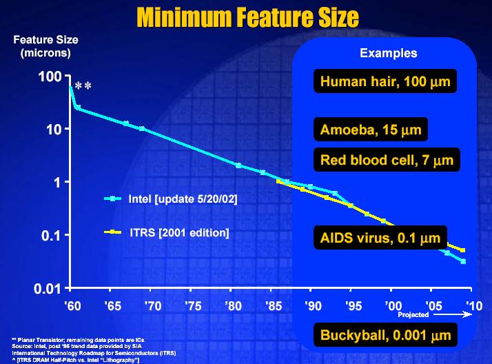
5 Moore s Law (Gordon Moore, Intel) exponentially more, cheaper, faster and smaller transistors Thomas Schenkel, Accelerator and Fusion Research

6 Moore s Law of exponential speedup of silicon transistors
7


8 Transistors The metal-oxide-semiconductor field-effect transistor (MOSFET) is the basic switching and amplification device of digital electronics. The current between the source and drain electrodes is controlled by the gate voltage. When the gate voltage is zero, no conduction electrons are present in the channel. When the gate is at a positive voltage, electrons from the source and drain accumulate in the area of the channel close to the gate. As the gate voltage is increased further, the number of electrons in the channel increases until saturation is reached. With no gate voltage, electrons in the channel experience a potential that is higher than the bias potential. As the gate voltage increases, the potential in the channel gradually lowers and electrons accumulate there. Thomas Schenkel, Accelerator and Fusion Research

9 Si-Lattice constant: 0.5 nm Cleavelin, TI, 03 Thomas Schenkel, Accelerator and Fusion Research
10 Why silicon? vastly abundant semiconductor that is easy to work with and that forms a great interface with a dielectric SiO 2 / Si interface has very low defect density (10 10 cm -2 V -1 ) very high degree of control over electrical properties allows larger scale integration compared to other materials with specific advantages: GaAs: direct band gap for opto-electronic integration (but: much harder to work with, forms poor interface to dielectric, no nuclear spin free isotopes ) diamond: larger band gap, ideal for high temperature operation (but difficult to make larger wafers, hard to dope, )

![3p 3 Si: [Ne].3s 2.](/docs-images/74/69741236/images/11-1.jpg "3p 2 one electron to")
11 The 31 P qubit in silicon P: [Ne].3s 2.3p 3 Si: [Ne].3s 2.3p 2 one electron to play with for P in Si
12 The 31 P qubit in silicon 31 P is a standard n-type dopant in silicon, one electron is ionized at room temperature and contributes to electrical conduction but at low temperature (<70 K), this electron remains bound to the P atom with a binding energy of 45 mev, and a Bohr radius of ~2.5 nm the spin of this electron in a global magnetic field is a very attractive two level system for quantum information processing, e. g., 0> = >, 1>= > the electron spin decoherence time is quite long, ~60 ms additionally, 31 P has a nuclear spin of I=1/2, while the nuclear spin of the silicon matrix can be prepared to be I=0 for isotopically pure 28 Si the nuclear spin can be addressed very precisely through hyperfine interaction, and nuclear spin decoherence times are very, very long (hours)
13 Criteria for physical implementation of a quantum computer (DiVincenzo) 1. Well defined extendible qubit array stable memory 2. Initialization in the 000 state 3. Long decoherence time (>10 4 operation time, to allow for error correction) 4. Universal set of gate operations (not, cnot) 5. Read-out: Single-quantum measurements (projective measurement) 31 P donor spins in silicon: natural quantum dots 20 to 200 nm Kane 98, 02: nuclear spin in 31 P as memory and spin coherent electron transport for two qubit operations, gate controlled hyperfine and exchange interactions Yablonovitch 00: e - spins and exchange interaction in Si x Ge y heterostructures Thomas Schenkel, Accelerator and Fusion Research
14 Solid state quantum computer scheme with 31 P in 28 Si (Kane 98) 31 P-qubit: gate controlled manipulation of single spins; nuclear spins store information, electron spins transfer information between neighboring qubits (J, exchange) and to nuclear spins (A=121.5 nev, hyperfine interaction) ( issues: J oscillations on Å length scale in Si; required control of hyperfine interaction
15
16 quantum information processing in a nutshell entangle ensembles of qubits (control) prevent interaction with environment (limit decoherence) run sequences of unitary operations on the ensemble read-out the end result in a projective measurement
17 Necessities for a spin quantum computer: 1. Long lived spin states 2. Single spin operations (Q NOT) controlled spin interactions with an external field 3. Two spin operations (Q CNOT) controlled interactions between spins 4. Single spin preparation and detection controlled interactions with external reservoirs Transistor model : Local gate control over single spins and two spin interaction
18 SINGLE SPIN OPERATIONS (QUANTUM NOT) Magnetic Resonance: In a magnetic field spin energy levels are split by an energy E=µB. An AC magnetic field will excite transitions between the two spin levels when hν= E If the AC field is turned on for the appropriate length of time, then the NOT operation is performed: ( & ) For nuclear spins at B=1 Tesla ν 10 MHz, For electron spin at B=1 Tesla ν 10 GHz, E 0.05 mev (T=0.5 K) Nuclear Resonance Frequency (MHz) Thomas Schenkel, Accelerator and Fusion Research 0 α=30 MHz/V V=0: A-Gate Barrier Si e - A-Gate Barrier Si V>0: A-Gate Barrier Si A-Gate Voltage (V) 31 P From Kane 99
19 Quantum Logic also requires CONTROLLED NOT operation on two spins. CNOT can be produced by EXCHANGE operation and NOT: EXCHANGE( )= EXCHANGE operation produced when two spins interact for a certain amount of time
20 TWO SPIN OPERATIONS (QUANTUM CNOT) Exchange Frequency (Hz) J=0: J-Gate A-Gate A-Gate - - J>0: B=2 T: J-Gate A-Gate A-Gate ++ 2µ B B/h=56 GHz Thomas Schenkel, Accelerator and Fusion Research Donor Separation (Å) From Kane 99

21 Hydrogenic spin quantum computing in silicon: a digital approach Thomas Schenkel, Accelerator and Fusion Research Skinner, Davenport, Kane 02 quant-ph/
22 Goal: Access the physics of the 31 P qubit in a scalable architecture QC-scheme & design testing fabrication
23 Solid state quantum computer development: A nano-fabrication challenge Bottom up Scanning probe hydrogen lithography epitaxial overgrowth, gate and readout structure formation Self assembly Top down Ion implantation into pre-fabricated structures aligned implantation followed by processing
24 Tools for Nanofabrication Scanning tunneling microscopy Hydrogen resist desorption with atomic resolution: ~0.2 nm Electron Beam Lithography Beam spot: ~5-10 nm, resolution limited by proximity effect: scattering of energetic (~100 kev) electrons in resist layers Ion Implantation Focused Ion Beam with Liquid Metal Ion Gun (Ga, In) Spot size: ~10 nm, 1 pa Shinada et al.: ~70 nm for 60 kev 31 P 2+ beam Low energy Single Ion Implantation Goal: 10 nm resolution at 1-10 KeV implant energy Status (11/03): 30 nm tests in progress, nano-stage with AFM (100 µm +/- 1 nm) being tested


25 Bottom up: STM hydrogen lithography J. O'Brien, et al., Univ. New South Wales, Sydney STM atom manipulation D. Eigler, et. co., IBM Desorption of H with low energy electrons (~10 ev) from the STM tip Advantage: atomic resolution Problems: encapsulation, dopant activation, device integration,.
26 Formation of integrated atom arrays by Single Ion Implantation plus some processing vision: to place individual ions (any element) into any solid with nm resolution (+/- 5 nm seems possible) tasks 1. Detect single ions Detection of secondary electron showers from deposition of potential energy of low energy (<20 kev), highly charged ions like 31 P Control spatial resolution Beam focusing and collimation Range straggling Diffusion during annealing, ensure electrical activation 3. Integrate with semiconductor processing Si nanowire Single Electron Transistor fabrication with Electron Beam Lithography and stress limited oxidation
27 Poissonian distribution of implanted ions Distribution of probabilities for implantation of ions where the implantation probability is small (<<1) for each incident ion and the number of ion impacts is large (>>1) At average, one ion is implanted. The probability for two adjacent ion hits is 13%

 (components not to")
28 Single ion implantation aligned with Scanning Probe highly charged ions ( 31 P 13+, 126 Te 34+, ) beam is blocked following one event and sample is moved to next qubit site Scanning Probe with hollow pyramid tip (~25 µm wide) detection of multiple secondary electrons from single ion hits registers impact events e - e - e - e - e - e - e - e - SP aligns implant beam to sample features (10 20 nm Si-SET lines) (components not to scale)

29 Single Ion Implanter with integrated Scanning Probe ion guide incident P 13+ or Te 33+ extraction and detection of secondary electron bursts Scanning Probe head with nano-aperture sample
30 Non-Poissonian single ion implantation with 31 P q+ P 12+ deposits 2.5 kev of potential energy, independent of kinetic energy emission of ~15 e - /P 12+, compared to about 1 e - /P 1+ from kinetic emission at E kin =10 kev Each ion impact is registered by detection of several secondary electrons 100% detection efficiency for single ions enables implantation of exact numbers of dopant ions focusing and collimation for pattern definition electron emission contrast enables imaging and alignment to markers for integration with consecutive E-beam lithography steps counts / channel copper SiO 2 /Si q18-phd-1 1 pulse height channel Pulse height distribution of secondary electrons from 31 P 12+ impacts on metal (blue) and silicon (native oxide on Si) (red) samples from an annular MCP detector
31 Secondary electron emission enables efficient detection of single ion impacts 160 secondary electrons / ion P Te42+ Au SiO 2 33pq potential energy (kev) Secondary electron yields from gold and SiO 2 targets as a function of potential energy of highly charged ions (Xe, Au and Th) with kinetic energies of 9kV q [T. Schenkel et al., NIM B 125, 153 (1997)]
32 P q+ beam formation 400 P 15+ P P 13+ F 8+ P 12+ P 11+ O 6+ F 7+ counts 200 O 8+ N 7+ F 9+ N 6+ N O q6-b-scans-p-1 5 mass / charge

33 The Electron Beam Ion Trap / Source beams of highly charged ions like P 15+, Te 42+, Xe 52+ and Au 69+ and kinetic energies from as low as 100 ev up to 1 MeV
 31 P 15+ at ~10 kev: interaction is dominated by deposition of potential")
34 Ion solid interactions with highly charged ions: femtosecond physics on a nanometer scale for v<v 0 and q>>q eq : hollow atom formation and decay electron capture Auger and radiative transitions collisions with target electrons and nuclei: energy loss Sputtering secondary electron emission lattice modifications (APL ) 31 P 15+ at ~10 kev: interaction is dominated by deposition of potential energy, equilibrium charge state, q eq = Z 1/3 v / v Bohr 0.3+ T. Schenkel et al., Prog. Surf. Sci. 61, 23 (1999); Phys. Rev. Lett. 83, 4273 (1999) Thomas Schenkel, Accelerator and Fusion Research

35 Straggling contributes to uncertainty in positioning of P-qubits 2 kev 5 kev Trajectories of P-ions in a-si simulated with the Monte Carlo code SRIM (Stopping and Range of Ions in Matter, Ziegler et al., IBM).


36 Single ion implantation setup


37 FEI Strata 235 dual beam FIB at LBNL etching oxide deposition Pt deposition


38 Piezoresistive Scanning Probe integration Piezoresistive SPM based on a Wheatstone bridge, and bimetallic actuation SPM test setup at LBNL co. I. Rangelow, University Kassel


39 Nanometer scale alignment accuracy through integration with SPM a 100 nm hole (shrink by thin film deposition) in a hollow tip on a piezo-resistive cantilever
40 Resolution limits in single ion implantation ? Etch pits in CR-39 from single 31 P 12+ impacts, not quite aligned yet mask opening: few nm wide holes with >10: 1 aspect ratios in thin SiN membranes P 12+ interaction with mask: image charge acceleration, e - capture, electronic sputtering

41 Device proposal: 31 P atoms aligned to Single Electron Transistors in silicon G Poly-Si A-G SG A-G S D Gate oxide Si 31 P 31 P S D S D SiO 2 Si Qubit spacing: ~50 to 100 nm SET pair in SOI, co. Alex Liddle, LBNL, and Jeff Bokor, UCB Single ion implantation, electron beam lithography and semiconductor processing for integration of 31 P qubits with gates and SET readout structures Si nanowire SETs formed in high temperature process prior to donor placement


42 Si-SETs in SOI with 10 nm line widths
43 SINGLE SPIN MEASUREMENT Intuition: An effective and rapid means of measuring single electron spins will rely on effective spin interactions that are a manifestation of the Pauli Principle, rather than on detecting a magnetic field generated by the electron spin. Ergo: Spin dependent charge measurements are promising path to single spin detection Pauli Exclusion Principle Overall wave-function of multi-electron system must be anti-symmetric with respect to particle interchange. For two spins there are three symmetric (triplet ) states:, +, and one antisymmetic (singlet) state: Exclusion Principle says that two electrons in the same orbital quantum state must be in a singlet spin state.
44 Coulomb blockade and single electron control Thomas Schenkel, Accelerator and Fusion Research Konstantin K. Likharev, IEEE, 99
45 Single electron transistor as a sensitive electrometer Gate controlled current flow I-V curves sensitive to local potential around island Alignment of SET with 31 P atoms allows spin dependent charge measurements charging energy for electrons to hop onto island: E c =e 2 /2C >> kt tunneling resistance R>>1/G=h/e 2 kohm need E c ~ 10 kt for reliable operation LHe, 4 K, kt = 0.34 mev SET at room temperature: capacitance of island ~1aF, size smaller than 10 nm Thomas Schenkel, Accelerator and Fusion Research
46 14 nm quantum wire SET measurements at 4K 4.E-09 3.E-09 2.E-09 1.E E+00-1.E-09-2.E-09-3.E-09-4.E mv
 Tunnel resistance 300kohm Total capacitance 10aF Gate capacitance 0.")
47 30 nm quantum wire SET measurements at 4K 3.05E E-08 Is-d(A) 2.E-08 1.E-08 0.E+00-1.E-08-2.E Vs-d(V) 2.95E-08 Is-d(A) 2.90E E E E Vg(V) Tunnel resistance 300kohm Total capacitance 10aF Gate capacitance 0.13aF Charging energy 8meV Is-d measurement through 30nm quantum wire at 10mV of Vs-d in the large plot And the same Is-d measurement with respect to Vs-d at two different Vg on top
48 Konstantin K. Likharev, IEEE, 99
49
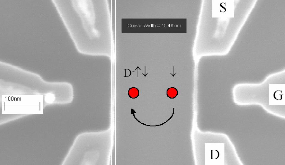
50 Basic building block to access the physics of the 31 P qubit: Two 31 P atoms aligned with control gates and SETs 20 to 100 nm Source Gate P P SET electrometer Drain Electron transfer into D - state for anti-parallel spins Gate control of single spins and read out through spin dependent charge transfer between 31 P atoms (based on singlet-triplet splitting and exclusion principle) (Kane 00)
51


52 Outlook: 31 P qubit physics by 2005, reach a QC test bed era by Kane, PRL, 03 Si-SETs Single ion implantation + + Process integration carrier concentration (e - /cm -3 ) 1E21 1E20 1E19 1E18 1E17 1E16 1E15 1E14 1E11 1E12 1E13 1E14 1E15 access quantum computation in silicon 1E depth (nm)
Towards quantum information processing with spins in silicon. Thomas Schenkel
 Towards quantum information processing with spins in silicon Thomas Schenkel E. O. Lawrence Berkeley National Laboratory T_Schenkel@LBL.gov http://www-ebit.lbl.gov/ Path to logic demonstrations with donor
Electron spin qubits in P donors in Silicon
 Electron spin qubits in P donors in Silicon IDEA League lectures on Quantum Information Processing 7 September 2015 Lieven Vandersypen http://vandersypenlab.tudelft.nl Slides with black background courtesy
Single ion implantation for nanoelectronics and the application to biological systems. Iwao Ohdomari Waseda University Tokyo, Japan
 Single ion implantation for nanoelectronics and the application to biological systems Iwao Ohdomari Waseda University Tokyo, Japan Contents 1.History of single ion implantation (SII) 2.Novel applications
Quantum control of spin qubits in silicon
 Quantum control of spin qubits in silicon Belita Koiller Instituto de Física Universidade Federal do Rio de Janeiro Brazil II Quantum Information Workshop Paraty, 8-11 September 2009 Motivation B.E.Kane,
How a single defect can affect silicon nano-devices. Ted Thorbeck
 How a single defect can affect silicon nano-devices Ted Thorbeck tedt@nist.gov The Big Idea As MOS-FETs continue to shrink, single atomic scale defects are beginning to affect device performance Gate Source
Quantum Information Processing with Semiconductor Quantum Dots
 Quantum Information Processing with Semiconductor Quantum Dots slides courtesy of Lieven Vandersypen, TU Delft Can we access the quantum world at the level of single-particles? in a solid state environment?
From nanophysics research labs to cell phones. Dr. András Halbritter Department of Physics associate professor
 From nanophysics research labs to cell phones Dr. András Halbritter Department of Physics associate professor Curriculum Vitae Birth: 1976. High-school graduation: 1994. Master degree: 1999. PhD: 2003.
Shallow Donors in Silicon as Electron and Nuclear Spin Qubits Johan van Tol National High Magnetic Field Lab Florida State University
 Shallow Donors in Silicon as Electron and Nuclear Spin Qubits Johan van Tol National High Magnetic Field Lab Florida State University Overview Electronics The end of Moore s law? Quantum computing Spin
Solid-State Spin Quantum Computers
 Solid-State Spin Quantum Computers 1 NV-Centers in Diamond P Donors in Silicon Kane s Computer (1998) P- doped silicon with metal gates Silicon host crystal + 31 P donor atoms + Addressing gates + J- coupling
Quantum Information Processing with Semiconductor Quantum Dots. slides courtesy of Lieven Vandersypen, TU Delft
 Quantum Information Processing with Semiconductor Quantum Dots slides courtesy of Lieven Vandersypen, TU Delft Can we access the quantum world at the level of single-particles? in a solid state environment?
Nanoelectronics. Topics
 Nanoelectronics Topics Moore s Law Inorganic nanoelectronic devices Resonant tunneling Quantum dots Single electron transistors Motivation for molecular electronics The review article Overview of Nanoelectronic
Ion Implantation. alternative to diffusion for the introduction of dopants essentially a physical process, rather than chemical advantages:
 Ion Implantation alternative to diffusion for the introduction of dopants essentially a physical process, rather than chemical advantages: mass separation allows wide varies of dopants dose control: diffusion
There's Plenty of Room at the Bottom
 There's Plenty of Room at the Bottom 12/29/1959 Feynman asked why not put the entire Encyclopedia Britannica (24 volumes) on a pin head (requires atomic scale recording). He proposed to use electron microscope
Lecture 2: Double quantum dots
 Lecture 2: Double quantum dots Basics Pauli blockade Spin initialization and readout in double dots Spin relaxation in double quantum dots Quick Review Quantum dot Single spin qubit 1 Qubit states: 450
MSN551 LITHOGRAPHY II
 MSN551 Introduction to Micro and Nano Fabrication LITHOGRAPHY II E-Beam, Focused Ion Beam and Soft Lithography Why need electron beam lithography? Smaller features are required By electronics industry:
 Image courtesy of Keith Schwab http://www.lbl.gov/science-articles/archive/afrd Articles/Archive/AFRD-quantum-logic.html http://www.wmi.badw.de/sfb631/tps/dqd2.gif http://qist.lanl.gov/qcomp_map.shtml
Lecture 8, April 12, 2017
 Lecture 8, April 12, 2017 This week (part 2): Semiconductor quantum dots for QIP Introduction to QDs Single spins for qubits Initialization Read-Out Single qubit gates Book on basics: Thomas Ihn, Semiconductor
Electrical Control of Single Spins in Semiconductor Quantum Dots Jason Petta Physics Department, Princeton University
 Electrical Control of Single Spins in Semiconductor Quantum Dots Jason Petta Physics Department, Princeton University g Q 2 m T + S Mirror U 3 U 1 U 2 U 3 Mirror Detector See Hanson et al., Rev. Mod. Phys.
Semiconductors: Applications in spintronics and quantum computation. Tatiana G. Rappoport Advanced Summer School Cinvestav 2005
 Semiconductors: Applications in spintronics and quantum computation Advanced Summer School 1 I. Background II. Spintronics Spin generation (magnetic semiconductors) Spin detection III. Spintronics - electron
Developing Quantum Logic Gates: Spin-Resonance-Transistors
 Developing Quantum Logic Gates: Spin-Resonance-Transistors H. W. Jiang (UCLA) SRT: a Field Effect Transistor in which the channel resistance monitors electron spin resonance, and the resonance frequency
Magnetic semiconductors. (Dilute) Magnetic semiconductors
 Magnetic semiconductors") Magnetic semiconductors We saw last time that: We d like to do spintronics in semiconductors, because semiconductors have many nice properties (gateability, controllable spin-orbit effects, long spin lifetimes).
Magnetic semiconductors We saw last time that: We d like to do spintronics in semiconductors, because semiconductors have many nice properties (gateability, controllable spin-orbit effects, long spin lifetimes).
Challenges for Materials to Support Emerging Research Devices
 Challenges for Materials to Support Emerging Research Devices C. Michael Garner*, James Hutchby +, George Bourianoff*, and Victor Zhirnov + *Intel Corporation Santa Clara, CA + Semiconductor Research Corporation
Single Electron Transistor (SET)
") Single Electron Transistor (SET) SET: e - e - dot A single electron transistor is similar to a normal transistor (below), except 1) the channel is replaced by a small dot. C g 2) the dot is separated from
Single Electron Transistor (SET) SET: e - e - dot A single electron transistor is similar to a normal transistor (below), except 1) the channel is replaced by a small dot. C g 2) the dot is separated from
STM spectroscopy (STS)
") STM spectroscopy (STS) di dv 4 e ( E ev, r) ( E ) M S F T F Basic concepts of STS. With the feedback circuit open the variation of the tunneling current due to the application of a small oscillating voltage
STM spectroscopy (STS) di dv 4 e ( E ev, r) ( E ) M S F T F Basic concepts of STS. With the feedback circuit open the variation of the tunneling current due to the application of a small oscillating voltage
Nova 600 NanoLab Dual beam Focused Ion Beam IITKanpur
 Nova 600 NanoLab Dual beam Focused Ion Beam system @ IITKanpur Dual Beam Nova 600 Nano Lab From FEI company (Dual Beam = SEM + FIB) SEM: The Electron Beam for SEM Field Emission Electron Gun Energy : 500
Lawrence Berkeley National Laboratory Lawrence Berkeley National Laboratory
 Lawrence Berkeley National Laboratory Lawrence Berkeley National Laboratory Title Single ion implantation for solid state quantum computer development Permalink https://escholarship.org/uc/item/0zb737fz
Progress towards the realization of quantum computer architectures in silicon and diamond. Thomas Schenkel. Lawrence Berkeley National Laboratory
 Progress towards the realization of quantum computer architectures in silicon and diamond Thomas Schenkel Lawrence Berkeley National Laboratory Contact: T_Schenkel@LBL.gov, 510-486-6674 CS-191, guest lecture,
Classification of Solids
 Classification of Solids Classification by conductivity, which is related to the band structure: (Filled bands are shown dark; D(E) = Density of states) Class Electron Density Density of States D(E) Examples
Energetic particles and their detection in situ (particle detectors) Part II. George Gloeckler
 Part II. George Gloeckler") Energetic particles and their detection in situ (particle detectors) Part II George Gloeckler University of Michigan, Ann Arbor, MI University of Maryland, College Park, MD Simple particle detectors Gas-filled
Energetic particles and their detection in situ (particle detectors) Part II George Gloeckler University of Michigan, Ann Arbor, MI University of Maryland, College Park, MD Simple particle detectors Gas-filled
Electrical Characterization with SPM Application Modules
 Electrical Characterization with SPM Application Modules Metrology, Characterization, Failure Analysis: Data Storage Magnetoresistive (MR) read-write heads Semiconductor Transistors Interconnect Ferroelectric
single-electron electron tunneling (SET)
") single-electron electron tunneling (SET) classical dots (SET islands): level spacing is NOT important; only the charging energy (=classical effect, many electrons on the island) quantum dots: : level spacing
single-electron electron tunneling (SET) classical dots (SET islands): level spacing is NOT important; only the charging energy (=classical effect, many electrons on the island) quantum dots: : level spacing
Molecular Electronics For Fun and Profit(?)
") Molecular Electronics For Fun and Profit(?) Prof. Geoffrey Hutchison Department of Chemistry University of Pittsburgh geoffh@pitt.edu July 22, 2009 http://hutchison.chem.pitt.edu Moore s Law: Transistor
Molecular Electronics For Fun and Profit(?) Prof. Geoffrey Hutchison Department of Chemistry University of Pittsburgh geoffh@pitt.edu July 22, 2009 http://hutchison.chem.pitt.edu Moore s Law: Transistor
Imaging Methods: Scanning Force Microscopy (SFM / AFM)
") Imaging Methods: Scanning Force Microscopy (SFM / AFM) The atomic force microscope (AFM) probes the surface of a sample with a sharp tip, a couple of microns long and often less than 100 Å in diameter.
Imaging Methods: Scanning Force Microscopy (SFM / AFM) The atomic force microscope (AFM) probes the surface of a sample with a sharp tip, a couple of microns long and often less than 100 Å in diameter.
Quantum physics in quantum dots
 Quantum physics in quantum dots Klaus Ensslin Solid State Physics Zürich AFM nanolithography Multi-terminal tunneling Rings and dots Time-resolved charge detection Moore s Law Transistors per chip 10 9
Some Key Materials Issues in Semiconductor Quantum Dots Based Nano-electronics
 Some Key Materials Issues in Semiconductor Quantum Dots Based Nano-electronics Prabhu Balasubramanian PhD Graduate Student Department of Materials Science and Engineering Rensselaer Polytechnic Institute,
Semiconductor Detectors
 Semiconductor Detectors Summary of Last Lecture Band structure in Solids: Conduction band Conduction band thermal conductivity: E g > 5 ev Valence band Insulator Charge carrier in conductor: e - Charge
Quantum Computation with Neutral Atoms Lectures 14-15
 Quantum Computation with Neutral Atoms Lectures 14-15 15 Marianna Safronova Department of Physics and Astronomy Back to the real world: What do we need to build a quantum computer? Qubits which retain
Lecture 3: Heterostructures, Quasielectric Fields, and Quantum Structures
 Lecture 3: Heterostructures, Quasielectric Fields, and Quantum Structures MSE 6001, Semiconductor Materials Lectures Fall 2006 3 Semiconductor Heterostructures A semiconductor crystal made out of more
Design Considerations for Integrated Semiconductor Control Electronics for a Large-scale Solid State Quantum Processor
 Design Considerations for Integrated Semiconductor Control Electronics for a Large-scale Solid State Quantum Processor Hendrik Bluhm Andre Kruth Lotte Geck Carsten Degenhardt 1 0 Ψ 1 Quantum Computing
what happens if we make materials smaller?
 what happens if we make materials smaller? IAP VI/10 ummer chool 2007 Couvin Prof. ns outline Introduction making materials smaller? ynthesis how do you make nanomaterials? Properties why would you make
2) Atom manipulation. Xe / Ni(110) Model: Experiment:
 Atom manipulation. Xe / Ni(110) Model: Experiment:") 2) Atom manipulation D. Eigler & E. Schweizer, Nature 344, 524 (1990) Xe / Ni(110) Model: Experiment: G.Meyer, et al. Applied Physics A 68, 125 (1999) First the tip is approached close to the adsorbate
2) Atom manipulation D. Eigler & E. Schweizer, Nature 344, 524 (1990) Xe / Ni(110) Model: Experiment: G.Meyer, et al. Applied Physics A 68, 125 (1999) First the tip is approached close to the adsorbate
MS482 Materials Characterization ( 재료분석 ) Lecture Note 5: RBS
 Lecture Note 5: RBS") 2016 Fall Semester MS482 Materials Characterization ( 재료분석 ) Lecture Note 5: RBS Byungha Shin Dept. of MSE, KAIST 1 Course Information Syllabus 1. Overview of various characterization techniques (1 lecture)
2016 Fall Semester MS482 Materials Characterization ( 재료분석 ) Lecture Note 5: RBS Byungha Shin Dept. of MSE, KAIST 1 Course Information Syllabus 1. Overview of various characterization techniques (1 lecture)
Electronic transport in low dimensional systems
 Electronic transport in low dimensional systems For example: 2D system l
ABSTRACT. Department of Physics. I present the results of experimental investigations into single electron transistors
 ABSTRACT Title of dissertation: MEASUREMENTS OF CHARGE MOTION IN SILICON WITH A SINGLE ELECTRON TRANSISTOR: TOWARD INDIVIDUAL DOPANT CONTROL Kenton Randolph Brown, Doctor of Philosophy, 2005 Dissertation
Institute for Electron Microscopy and Nanoanalysis Graz Centre for Electron Microscopy
 Institute for Electron Microscopy and Nanoanalysis Graz Centre for Electron Microscopy Micromechanics Ass.Prof. Priv.-Doz. DI Dr. Harald Plank a,b a Institute of Electron Microscopy and Nanoanalysis, Graz
Chapter 3 Properties of Nanostructures
 Chapter 3 Properties of Nanostructures In Chapter 2, the reduction of the extent of a solid in one or more dimensions was shown to lead to a dramatic alteration of the overall behavior of the solids. Generally,
Lecture 6. Alternative storage technologies. All optical recording. Racetrack memory. Topological kink solitons. Flash memory. Holographic memory
 Lecture 6 Alternative storage technologies All optical recording Racetrack memory Topological kink solitons Flash memory Holographic memory Millipede Ferroelectric memory All-optical recording It is possible
arxiv:cond-mat/ v1 [cond-mat.mtrl-sci] 26 Feb 2004
![arxiv:cond-mat/ v1 [cond-mat.mtrl-sci] 26 Feb 2004](/thumbs/72/66342523.jpg "arxiv:cond-mat/ v1 [cond-mat.mtrl-sci] 26 Feb 2004") Voltage Control of Exchange Coupling in Phosphorus Doped Silicon arxiv:cond-mat/42642v1 [cond-mat.mtrl-sci] 26 Feb 24 C.J. Wellard a, L.C.L. Hollenberg a, L.M. Kettle b and H.-S. Goan c Centre for Quantum
Voltage Control of Exchange Coupling in Phosphorus Doped Silicon arxiv:cond-mat/42642v1 [cond-mat.mtrl-sci] 26 Feb 24 C.J. Wellard a, L.C.L. Hollenberg a, L.M. Kettle b and H.-S. Goan c Centre for Quantum
The Development of a Quantum Computer in Silicon
 The Development of a Quantum Computer in Silicon Professor Michelle Simmons Director, Centre of Excellence for Quantum Computation and Communication Technology, Sydney, Australia December 4th, 2013 Outline
Minimal Update of Solid State Physics
 Minimal Update of Solid State Physics It is expected that participants are acquainted with basics of solid state physics. Therefore here we will refresh only those aspects, which are absolutely necessary
Surfaces, Interfaces, and Layered Devices
 Surfaces, Interfaces, and Layered Devices Building blocks for nanodevices! W. Pauli: God made solids, but surfaces were the work of Devil. Surfaces and Interfaces 1 Interface between a crystal and vacuum
Fabrication / Synthesis Techniques
 Quantum Dots Physical properties Fabrication / Synthesis Techniques Applications Handbook of Nanoscience, Engineering, and Technology Ch.13.3 L. Kouwenhoven and C. Marcus, Physics World, June 1998, p.35
phys4.20 Page 1 - the ac Josephson effect relates the voltage V across a Junction to the temporal change of the phase difference
 Josephson Effect - the Josephson effect describes tunneling of Cooper pairs through a barrier - a Josephson junction is a contact between two superconductors separated from each other by a thin (< 2 nm)
Single atom doping for quantum device development in diamond and silicon
 Single atom doping for quantum device development in diamond and silicon C. D. Weis and A. Schuh Lawrence Berkeley National Laboratory, 1 Cyclotron Road, Berkeley, California 94114 and Technical University
Formation of unintentional dots in small Si nanostructures
 Superlattices and Microstructures, Vol. 28, No. 5/6, 2000 doi:10.1006/spmi.2000.0942 Available online at http://www.idealibrary.com on Formation of unintentional dots in small Si nanostructures L. P. ROKHINSON,
ABSTRACT. Department of Physics. a narrow ( 100 nm) metal-oxide-semiconductor field-effect transistor (MOSFET).
 metal-oxide-semiconductor field-effect transistor (MOSFET).") ABSTRACT Title of dissertation: CHARACTERIZATION OF METAL-OXIDE-SEMICONDUCTOR STRUCTURES AT LOW TEMPERATURES USING SELF-ALIGNED AND VERTICALLY COUPLED ALUMINUM AND SILICON SINGLE-ELECTRON TRANSISTORS Luyan
ABSTRACT Title of dissertation: CHARACTERIZATION OF METAL-OXIDE-SEMICONDUCTOR STRUCTURES AT LOW TEMPERATURES USING SELF-ALIGNED AND VERTICALLY COUPLED ALUMINUM AND SILICON SINGLE-ELECTRON TRANSISTORS Luyan
Stretching the Barriers An analysis of MOSFET Scaling. Presenters (in order) Zeinab Mousavi Stephanie Teich-McGoldrick Aseem Jain Jaspreet Wadhwa
 Zeinab Mousavi Stephanie Teich-McGoldrick Aseem Jain Jaspreet Wadhwa") Stretching the Barriers An analysis of MOSFET Scaling Presenters (in order) Zeinab Mousavi Stephanie Teich-McGoldrick Aseem Jain Jaspreet Wadhwa Why Small? Higher Current Lower Gate Capacitance Higher
Stretching the Barriers An analysis of MOSFET Scaling Presenters (in order) Zeinab Mousavi Stephanie Teich-McGoldrick Aseem Jain Jaspreet Wadhwa Why Small? Higher Current Lower Gate Capacitance Higher
Carbon Nanotubes in Interconnect Applications
 Carbon Nanotubes in Interconnect Applications Page 1 What are Carbon Nanotubes? What are they good for? Why are we interested in them? - Interconnects of the future? Comparison of electrical properties
Temperature dependence of spin diffusion length in silicon by Hanle-type spin. precession
 Temperature dependence of spin diffusion length in silicon by Hanle-type spin precession T. Sasaki 1,a), T. Oikawa 1, T. Suzuki 2, M. Shiraishi 3, Y. Suzuki 3, and K. Noguchi 1 SQ Research Center, TDK
Interaction of ion beams with matter
 Interaction of ion beams with matter Introduction Nuclear and electronic energy loss Radiation damage process Displacements by nuclear stopping Defects by electronic energy loss Defect-free irradiation
Multiple Gate CMOS and Beyond
 Multiple CMOS and Beyond Dept. of EECS, KAIST Yang-Kyu Choi Outline 1. Ultimate Scaling of MOSFETs - 3nm Nanowire FET - 8nm Non-Volatile Memory Device 2. Multiple Functions of MOSFETs 3. Summary 2 CMOS
Terahertz sensing and imaging based on carbon nanotubes:
 Terahertz sensing and imaging based on carbon nanotubes: Frequency-selective detection and near-field imaging Yukio Kawano RIKEN, JST PRESTO ykawano@riken.jp http://www.riken.jp/lab-www/adv_device/kawano/index.html
NBTI and Spin Dependent Charge Pumping in 4H-SiC MOSFETs
 NBTI and Spin Dependent Charge Pumping in 4H-SiC MOSFETs Mark A. Anders, Patrick M. Lenahan, Pennsylvania State University Aivars Lelis, US Army Research Laboratory Energy Deviations from the resonance
Fabrication Technology, Part I
 EEL5225: Principles of MEMS Transducers (Fall 2004) Fabrication Technology, Part I Agenda: Microfabrication Overview Basic semiconductor devices Materials Key processes Oxidation Thin-film Deposition Reading:
Gold Nanoparticles Floating Gate MISFET for Non-Volatile Memory Applications
 Gold Nanoparticles Floating Gate MISFET for Non-Volatile Memory Applications D. Tsoukalas, S. Kolliopoulou, P. Dimitrakis, P. Normand Institute of Microelectronics, NCSR Demokritos, Athens, Greece S. Paul,
Self-study problems and questions Processing and Device Technology, FFF110/FYSD13
 Self-study problems and questions Processing and Device Technology, FFF110/FYSD13 Version 2016_01 In addition to the problems discussed at the seminars and at the lectures, you can use this set of problems
Instrumentation and Operation
 Instrumentation and Operation 1 STM Instrumentation COMPONENTS sharp metal tip scanning system and control electronics feedback electronics (keeps tunneling current constant) image processing system data
Nanoelectronics 09. Atsufumi Hirohata Department of Electronics. Quick Review over the Last Lecture
 Nanoelectronics 09 Atsufumi Hirohata Department of Electronics 13:00 Monday, 12/February/2018 (P/T 006) Quick Review over the Last Lecture ( Field effect transistor (FET) ): ( Drain ) current increases
Scanning Tunneling Microscopy
 Scanning Tunneling Microscopy References: 1. G. Binnig, H. Rohrer, C. Gerber, and Weibel, Phys. Rev. Lett. 49, 57 (1982); and ibid 50, 120 (1983). 2. J. Chen, Introduction to Scanning Tunneling Microscopy,
Large Storage Window in a-sinx/nc-si/a-sinx Sandwiched Structure
 2017 Asia-Pacific Engineering and Technology Conference (APETC 2017) ISBN: 978-1-60595-443-1 Large Storage Window in a-sinx/nc-si/a-sinx Sandwiched Structure Xiang Wang and Chao Song ABSTRACT The a-sin
2.0 Basic Elements of a Quantum Information Processor. 2.1 Classical information processing The carrier of information
 QSIT09.L03 Page 1 2.0 Basic Elements of a Quantum Information Processor 2.1 Classical information processing 2.1.1 The carrier of information - binary representation of information as bits (Binary digits).
EE 5344 Introduction to MEMS CHAPTER 5 Radiation Sensors
 EE 5344 Introduction to MEMS CHAPTER 5 Radiation Sensors 5. Radiation Microsensors Radiation µ-sensors convert incident radiant signals into standard electrical out put signals. Radiant Signals Classification
Quantum Computation 650 Spring 2009 Lectures The World of Quantum Information. Quantum Information: fundamental principles
 Quantum Computation 650 Spring 2009 Lectures 1-21 The World of Quantum Information Marianna Safronova Department of Physics and Astronomy February 10, 2009 Outline Quantum Information: fundamental principles
Single Electron Transistor (SET)
") Single Electron Transistor (SET) e - e - dot C g V g A single electron transistor is similar to a normal transistor (below), except 1) the channel is replaced by a small dot. 2) the dot is separated from
Single Electron Transistor (SET) e - e - dot C g V g A single electron transistor is similar to a normal transistor (below), except 1) the channel is replaced by a small dot. 2) the dot is separated from
Chap. 1 (Introduction), Chap. 2 (Components and Circuits)
, Chap. 2 (Components and Circuits)") CHEM 455 The class describes the principles and applications of modern analytical instruments. Emphasis is placed upon the theoretical basis of each type of instrument, its optimal area of application,
CHEM 455 The class describes the principles and applications of modern analytical instruments. Emphasis is placed upon the theoretical basis of each type of instrument, its optimal area of application,
Saroj P. Dash. Chalmers University of Technology. Göteborg, Sweden. Microtechnology and Nanoscience-MC2
 Silicon Spintronics Saroj P. Dash Chalmers University of Technology Microtechnology and Nanoscience-MC2 Göteborg, Sweden Acknowledgement Nth Netherlands University of Technology Sweden Mr. A. Dankert Dr.
EE130: Integrated Circuit Devices
 EE130: Integrated Circuit Devices (online at http://webcast.berkeley.edu) Instructor: Prof. Tsu-Jae King (tking@eecs.berkeley.edu) TA s: Marie Eyoum (meyoum@eecs.berkeley.edu) Alvaro Padilla (apadilla@eecs.berkeley.edu)
EE143 LAB. Professor N Cheung, U.C. Berkeley
 EE143 LAB 1 1 EE143 Equipment in Cory 218 2 Guidelines for Process Integration * A sequence of Additive and Subtractive steps with lateral patterning Processing Steps Si wafer Watch out for materials compatibility
Introduction into Positron Annihilation
 Introduction into Positron Annihilation Introduction (How to get positrons? What is special about positron annihilation?) The methods of positron annihilation (positron lifetime, Doppler broadening, ACAR...)
ESE370: Circuit-Level Modeling, Design, and Optimization for Digital Systems
 ESE370: Circuit-Level Modeling, Design, and Optimization for Digital Systems Lec 6: September 18, 2017 MOS Model You are Here: Transistor Edition! Previously: simple models (0 and 1 st order) " Comfortable
Chapter 12: Electrical Properties. RA l
 Charge carriers and conduction: Chapter 12: Electrical Properties Charge carriers include all species capable of transporting electrical charge, including electrons, ions, and electron holes. The latter
SUPPLEMENTARY INFORMATION
 Electrical control of single hole spins in nanowire quantum dots V. S. Pribiag, S. Nadj-Perge, S. M. Frolov, J. W. G. van den Berg, I. van Weperen., S. R. Plissard, E. P. A. M. Bakkers and L. P. Kouwenhoven
Quantum Dots: Artificial Atoms & Molecules in the Solid-State
 Network for Computational Nanotechnology (NCN) Purdue, Norfolk State, Northwestern, UC Berkeley, Univ. of Illinois, UTEP Quantum Dots: Artificial Atoms & Molecules in the Solid-State Network for Computational
Transport through Andreev Bound States in a Superconductor-Quantum Dot-Graphene System
 Transport through Andreev Bound States in a Superconductor-Quantum Dot-Graphene System Nadya Mason Travis Dirk, Yung-Fu Chen, Cesar Chialvo Taylor Hughes, Siddhartha Lal, Bruno Uchoa Paul Goldbart University
Lecture 0: Introduction
 Lecture 0: Introduction Introduction q Integrated circuits: many transistors on one chip q Very Large Scale Integration (VLSI): bucketloads! q Complementary Metal Oxide Semiconductor Fast, cheap, low power
MS482 Materials Characterization ( 재료분석 ) Lecture Note 5: RBS. Byungha Shin Dept. of MSE, KAIST
 Lecture Note 5: RBS. Byungha Shin Dept. of MSE, KAIST") 2015 Fall Semester MS482 Materials Characterization ( 재료분석 ) Lecture Note 5: RBS Byungha Shin Dept. of MSE, KAIST 1 Course Information Syllabus 1. Overview of various characterization techniques (1 lecture)
2015 Fall Semester MS482 Materials Characterization ( 재료분석 ) Lecture Note 5: RBS Byungha Shin Dept. of MSE, KAIST 1 Course Information Syllabus 1. Overview of various characterization techniques (1 lecture)
(a) (b) Supplementary Figure 1. (a) (b) (a) Supplementary Figure 2. (a) (b) (c) (d) (e)
 (b) Supplementary Figure 1. (a) (b) (a) Supplementary Figure 2. (a) (b) (c) (d) (e)") (a) (b) Supplementary Figure 1. (a) An AFM image of the device after the formation of the contact electrodes and the top gate dielectric Al 2 O 3. (b) A line scan performed along the white dashed line
(a) (b) Supplementary Figure 1. (a) An AFM image of the device after the formation of the contact electrodes and the top gate dielectric Al 2 O 3. (b) A line scan performed along the white dashed line
MSE 321 Structural Characterization
 Auger Spectroscopy Auger Electron Spectroscopy (AES) Scanning Auger Microscopy (SAM) Incident Electron Ejected Electron Auger Electron Initial State Intermediate State Final State Physical Electronics
There s plenty of room at the bottom! - R.P. Feynman, Nanostructure: a piece of material with at least one dimension less than 100 nm in extent.
 Nanostructures and Nanotechnology There s plenty of room at the bottom! - R.P. Feynman, 1959 Materials behave differently when structured at the nm scale than they do in bulk. Technologies now exist that
Spintronics. Seminar report SUBMITTED TO: SUBMITTED BY:
 A Seminar report On Spintronics Submitted in partial fulfillment of the requirement for the award of degree of Electronics SUBMITTED TO: SUBMITTED BY: www.studymafia.org www.studymafia.org Preface I have
Split gate tunnel barriers in double top gated silicon metal-oxide-semiconductor nanostructures
 University of New Mexico UNM Digital Repository Electrical and Computer Engineering ETDs Engineering ETDs 1-30-2013 Split gate tunnel barriers in double top gated silicon metal-oxide-semiconductor nanostructures
IV. Surface analysis for chemical state, chemical composition
 IV. Surface analysis for chemical state, chemical composition Probe beam Detect XPS Photon (X-ray) Photoelectron(core level electron) UPS Photon (UV) Photoelectron(valence level electron) AES electron
Self-Assembled InAs Quantum Dots
 Self-Assembled InAs Quantum Dots Steve Lyon Department of Electrical Engineering What are semiconductors What are semiconductor quantum dots How do we make (grow) InAs dots What are some of the properties
Semiconductor Device Physics
 1 Semiconductor Device Physics Lecture 3 http://zitompul.wordpress.com 2 0 1 3 Semiconductor Device Physics 2 Three primary types of carrier action occur inside a semiconductor: Drift: charged particle
Make sure the exam paper has 9 pages (including cover page) + 3 pages of data for reference
 + 3 pages of data for reference") UNIVERSITY OF CALIFORNIA College of Engineering Department of Electrical Engineering and Computer Sciences Spring 2006 EE143 Midterm Exam #1 Family Name First name SID Signature Make sure the exam paper
UNIVERSITY OF CALIFORNIA College of Engineering Department of Electrical Engineering and Computer Sciences Spring 2006 EE143 Midterm Exam #1 Family Name First name SID Signature Make sure the exam paper
Determination of the tunnel rates through a few-electron quantum dot
 Determination of the tunnel rates through a few-electron quantum dot R. Hanson 1,I.T.Vink 1, D.P. DiVincenzo 2, L.M.K. Vandersypen 1, J.M. Elzerman 1, L.H. Willems van Beveren 1 and L.P. Kouwenhoven 1
JFET/MESFET. JFET: small gate current (reverse leakage of the gate-to-channel junction) More gate leakage than MOSFET, less than bipolar.
 More gate leakage than MOSFET, less than bipolar.") JFET/MESFET JFET: small gate current (reverse leakage of the gate-to-channel junction) More gate leakage than MOSFET, less than bipolar. JFET has higher transconductance than the MOSFET. Used in low-noise,
JFET/MESFET JFET: small gate current (reverse leakage of the gate-to-channel junction) More gate leakage than MOSFET, less than bipolar. JFET has higher transconductance than the MOSFET. Used in low-noise,
Quantum-dot cellular automata
 Quantum-dot cellular automata G. L. Snider, a) A. O. Orlov, I. Amlani, X. Zuo, G. H. Bernstein, C. S. Lent, J. L. Merz, and W. Porod Department of Electrical Engineering, University of Notre Dame, Notre
SUPPLEMENTARY NOTES Supplementary Note 1: Fabrication of Scanning Thermal Microscopy Probes
 SUPPLEMENTARY NOTES Supplementary Note 1: Fabrication of Scanning Thermal Microscopy Probes Fabrication of the scanning thermal microscopy (SThM) probes is summarized in Supplementary Fig. 1 and proceeds
Nanoimprint Lithography
 Nanoimprint Lithography Wei Wu Quantum Science Research Advanced Studies HP Labs, Hewlett-Packard Email: wei.wu@hp.com Outline Background Nanoimprint lithography Thermal based UV-based Applications based