Electron transport : From nanoparticle arrays to single nanoparticles. Hervé Aubin
|
|
|
- Erick Boone
- 5 years ago
- Views:
Transcription

1 Electron transport : From nanoparticle arrays to single nanoparticles Hervé Aubin
 Limin Cui")
 Alexandre")

 V.")


2 Qian Yu (PhD) Hongyue Wang (PhD) Helena Moreira (PhD) Limin Cui (Visitor) Irena Resa(Post-doc) Brice Nadal (Post-doc) Alexandre Zimmers (MdC) Hervé Aubin (CR) C. Ulysse LPN (Microfabrication Facility) M. Rosticher ENS (Clean Room) V. Rebuttini N. Pinna Fe 3 O 4 Humboldt University (Berlin) E. Lhullier B. Dubertret PbS, PbSe LPEM - ESPCI D. Portehault C. Sanchez Ti 4 O 7 LCMCP Collège de France
3 SUMMARY Part I Transport in nanoparticle arrays Electron transport in disordered systems Doped semiconductors against granular metals Co-tunneling transport in gold nanoparticles arrays Efros-Shklovskii and Middleton-Wingreen Part II Transport in single nanoparticle devices In-Vacuum projection of nanoparticles for on-chip tunneling spectroscopy Verwey transition in single magnetite nanoparticles


4 Variable Range Hopping in semiconductors VRH Laws exp ( T / ) Mean Level Spacing TMott 0 0 Mott Law 1/ T Efros-Shklovskii Law Hot Hopping regime Cold Coulomb Energy T ES 2 e 1/ 2

5 Efros-Shklovskii law in bulk semiconduting CdSe Zhang, Y. et al. Probing the Coulomb Gap in Insulating n-type CdSe. Physical Review Letters 1990, 64,
6 Efros-Shklovskii law in semiconduting CdSe nanoparticles films Yu, D.et al. Variable Range Hopping Conduction in Semiconductor Nanocrystal Solids. Physical Review Letters 2004, 92,
.")
7 Evaporated metal thin films Platinum film between 0.1 nm and 10 nm thick 1.Neugebauer et al. JAP 33, 74 (1962). Coulomb energy () r Q 4 r 0 C Q 4 r self 0 E C e e e r 2C self
8 Efros-Shklovskii law in disordered metal thin films!!! 1.Sheng, P., Abeles, Ni films Physical Review Letters 31, (1973). 1/2 0exp( ( T0 / T) ) Simon, R. et al. granular niobium nitride cermet films Physical Review B 36, (1987).


 Arrays")

9 Electron transport in metallic nanocrystals arrays - sample preparation Synthesis - Brust method(1992) - Revisited by Klabunde (1998) Arrays crosslinked by alcane dithiol molecules 5nm Arrays formed by the Langmuir method
 100 1 0.01 1E-4 1E-6-10 0 10 100 50 Bias (V) 25 exp( T / T) 0 0 Activated law 0.02 0.04 0.")
10 Conductance (ns) Current (na) Electron transport in nanocrystals arrays (as function of temperature) 4 2 C6S 45 K 20 K r C Q 4 r self K -4 Coulomb energy 2 e 2 EC k BT0 e /40r 2C self 1100K ( r 2.5 nm, 3) E-4 1E Bias (V) 25 exp( T / T) 0 0 Activated law Temperature (K -1 )
11 Conductance (ns) Efros-Shklovskii law in nanocrystals arrays (as function of temperature) At larger quantum tunnel coupling, and low temperature, the conductance follows the variable range hopping law of Efros- Shklovskii. exp( / ) 0 TES T T 8000K ES 1/ d 25 C6S C2S2 C4S2 C6S2 C8S C8S2 exp(-t 0 /T) exp(-t ES /T) 1/2 ES law E-4 Activated law Temperature (K -1 ) 1E-6
 1.Tran, T.B. et al.")
12 Efros-Shklovskii law in nanocrystals array H. Jaeger s group (Chicago) 1.Tran, T.B. et al. Physical Review Letters 95, (2005).


13 Why is Efros-Shklovskii law in granular metallic systems surprising? In semiconductors, direct long distance tunneling is possible Long distance tunneling between metallic grains is not possible
14 «co-tunneling» At low temperature, electron transport is blocked because of the large Coulomb energy E c =e 2 /2C As tunnel coupling between the nanocrystal and the electrodes becomes large, electron tunneling through virtual charged states become possible. This is cotunneling.
15 Efros-Shklovskii law in granular metals explained by «co-tunneling» Single long distance tunneling is not possible Simultaneous multiple short distance tunneling events is possible [1] Jingshan Zhang and Boris I. Shklovskii, Physical Review B 70, (2004) [2] M.V. Feigel man and A.S. Ioselevich, Jetp Letters 81, 277 (2005) [3] I. Beloborodov, A. Lopatin, and V. Vinokur, Physical Review B 72, (2005). [4] I. S. Beloborodov, A. V. Lopatin, V. M. Vinokur, and K. B. Efetov, Reviews of Modern Physics 79, (2007).

 ) 0 ECoulomb kbt Short")
 T I I exp( ( / ) ) 0")
16 Electron transport in nanocrystals arrays (as function of electric field) Long Screening length I I exp( ( / ) ) 0 ECoulomb kbt Short Screening length Middleton-Wingreen I ( V V ) T I I exp( ( / ) ) 0 ECoulomb ev Insulator
17 In our arrays, Long Screening length model applies Weak capacitive coupling with the gate Short distance between electrodes ~150 nm Threshold voltage is not relevant
18 Electron transport in nanocrystals arrays (as function of electric field) For weakly conducting NC arrays, i.e. small tunnel barrier transparency, the I(V) curve follows an activated law, dotted line. Activated law ES law For better conducting arrays, i.e. for larger tunnel barrier transparency, the I(V) curve follows an ES-type law, dashed line H. Moreira et al. Physical Review Letters 107, (2011)


19 Toward single nanoparticle spectroscopy Bulk transitions Spectral characteristics of single nanoparticles Anderson Localization Thouless energy Mott Localization Coulomb energy Superconductor-Insulator Transition Superconducting gap
20 Nanoparticles Trapping Goal Trapping a single nanoparticle within the nanogap, (with no parasitic current path) The success rate should be high enough so that the technique can be applied to many different chemically synthesized nanoparticles Can be done in inert atmosphere (argon) Method 1 : Electrostatic or molecular assembly in solution Method 2 : Method 1+ Dielectrophoretic Force Method 3 : nanolithography + one of the other method avoid methods in solution, because of the impossibility of checking tunnel current during assembly Method 4 : High vacuum projection of nanoparticles


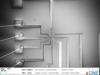

21 Wafer de nanogaps (LPN Microfab facility)

22 Method 4: In-vacuum projection of nanoparticles High vacuum chamber used for the projection of nanoparticles on the chip, using a fast pulsed valve( reponse time ~1 ms).
23 Projection curve opening of the valve < 1 ms bias voltage = 0.1 V Current measured 10s after the projection Threshold=0.01nA
24 Single gold nanoparticle trapped within the nanogap signatures of Coulomb blockade Yu, Q et al. ACS nano 2013, 7,

25 R (cm) Verwey transition in magnetite (Fe 3 O 4 ) Site A Site B O T v = 120K Temperature (K)


26 Verwey transition in single magnetite nanoparticles


27 Verwey transition in single magnetite nanoparticles d 15 nm E V = V V d = V cm 1 a = nm potential depth : V t = E V a 9.8 mev.

28 Folwer-Nordheim Plot T>T Verwey T<T Verwey
29 CONCLUSIONS Effective long distance hopping in metallic nanoparticles arrays is possible because of cotunneling Efros-Shklovskii laws applies in metallic nanoparticles arrays as a function of temperature, but also as function of electric field. A new projection method of preparing single nanoparticles devices Allows to study non-equilibrium Verwey transition in magnetite

30 Contributions to Folwer-Nordheim plot

31 Verwey transition in single magnetite nanoparticles
32 Tunneling spectroscopy of nanoparticles To study the construction of band structures with discrete electronic levels Semi-conductors (strong quantum confinement effects) Metals (fractal wave functions, random matric theory and relation with Anderson localization) Semi-metals (no studies so far) Mott Insulator (no studies so far) Superconductors (only a few works)
 CdSe/CdS (c)")
 Au-CdSe-Au rods (f)")

33 A plethora of nanoparticles (a) CdSe/CdS nanorods (b) CdSe/CdS (c) Au/PbS core-shells (d) CoPt 3 -Au dumbbells (e) Au-CdSe-Au rods (f) CdS-Au2S segmented nanoheterostructures. Talapin et al. Chem. Rev. 2010, 110, 389
34 Electron transport in granular films (Ni- SiO 2 ) as function of electric field Sheng, P. & Abeles, B. Physical Review Letters 28, 34-37(1972). Acivated law as function of electric field I I exp( / ) 0 ECoulomb ev
arxiv:cond-mat/ v2 [cond-mat.mes-hall] 25 Jun 2005
![arxiv:cond-mat/ v2 [cond-mat.mes-hall] 25 Jun 2005](/thumbs/78/76852456.jpg "arxiv:cond-mat/ v2 [cond-mat.mes-hall] 25 Jun 2005") Multiple Cotunneling in Large Quantum Dot Arrays T. B. Tran 1, I. S. Beloborodov 2, X. M. Lin 2,3, V. M. Vinokur 2, and H. M. Jaeger 1 arxiv:cond-mat/0505143v2 [cond-mat.mes-hall] 25 Jun 2005 1 James Franck
Multiple Cotunneling in Large Quantum Dot Arrays T. B. Tran 1, I. S. Beloborodov 2, X. M. Lin 2,3, V. M. Vinokur 2, and H. M. Jaeger 1 arxiv:cond-mat/0505143v2 [cond-mat.mes-hall] 25 Jun 2005 1 James Franck
Introduction to Nanotechnology Chapter 5 Carbon Nanostructures Lecture 1
 Introduction to Nanotechnology Chapter 5 Carbon Nanostructures Lecture 1 ChiiDong Chen Institute of Physics, Academia Sinica chiidong@phys.sinica.edu.tw 02 27896766 Carbon contains 6 electrons: (1s) 2,
Temperature dependence of Andreev spectra in a superconducting carbon nanotube quantum dot
 Temperature dependence of Andreev spectra in a superconducting carbon nanotube quantum dot A. Kumar, M. Gaim, D. Steininger, A. Levy Yeyati, A. Martín-Rodero, A. K. Hüttel, and C. Strunk Phys. Rev. B 89,
Defense Technical Information Center Compilation Part Notice
 UNCLASSIFIED Defense Technical Information Center Compilation Part Notice ADP013285 TITLE: On the Conduction Mechanism in Granular Materials DISTRIBUTION: Approved for public release, distribution unlimited
single-electron electron tunneling (SET)
") single-electron electron tunneling (SET) classical dots (SET islands): level spacing is NOT important; only the charging energy (=classical effect, many electrons on the island) quantum dots: : level spacing
single-electron electron tunneling (SET) classical dots (SET islands): level spacing is NOT important; only the charging energy (=classical effect, many electrons on the island) quantum dots: : level spacing
what happens if we make materials smaller?
 what happens if we make materials smaller? IAP VI/10 ummer chool 2007 Couvin Prof. ns outline Introduction making materials smaller? ynthesis how do you make nanomaterials? Properties why would you make
Chapter 7 A revised variable-range hopping model explains the peculiar T-dependence of electronic conductivity in ZnO quantum-dot solids
 A revised variable-range hopping model explains the peculiar T-dependence of electronic conductivity in ZnO quantum-dot solids The temperature dependence of electrical conductivity of assemblies of ZnO
Herre van der Zant. interplay between molecular spin and electron transport (molecular spintronics) Gate
 Gate") transport through the single molecule magnet Mn12 Herre van der Zant H.B. Heersche, Z. de Groot (Delft) C. Romeike, M. Wegewijs (RWTH Aachen) D. Barreca, E. Tondello (Padova) L. Zobbi, A. Cornia (Modena)
transport through the single molecule magnet Mn12 Herre van der Zant H.B. Heersche, Z. de Groot (Delft) C. Romeike, M. Wegewijs (RWTH Aachen) D. Barreca, E. Tondello (Padova) L. Zobbi, A. Cornia (Modena)
Single Electron Tunneling Examples
 Single Electron Tunneling Examples Danny Porath 2002 (Schönenberger et. al.) It has long been an axiom of mine that the little things are infinitely the most important Sir Arthur Conan Doyle Books and
Transport through Andreev Bound States in a Superconductor-Quantum Dot-Graphene System
 Transport through Andreev Bound States in a Superconductor-Quantum Dot-Graphene System Nadya Mason Travis Dirk, Yung-Fu Chen, Cesar Chialvo Taylor Hughes, Siddhartha Lal, Bruno Uchoa Paul Goldbart University
Spatially resolving density-dependent screening around a single charged atom in graphene
 Supplementary Information for Spatially resolving density-dependent screening around a single charged atom in graphene Dillon Wong, Fabiano Corsetti, Yang Wang, Victor W. Brar, Hsin-Zon Tsai, Qiong Wu,
Three-terminal quantum-dot thermoelectrics
 Three-terminal quantum-dot thermoelectrics Björn Sothmann Université de Genève Collaborators: R. Sánchez, A. N. Jordan, M. Büttiker 5.11.2013 Outline Introduction Quantum dots and Coulomb blockade Quantum
not to be confused with using the materials to template nanostructures
 Zeolites as Templates: continued Synthesis: Most zeolite syntheses are performed by using template-synthesis not to be confused with using the materials to template nanostructures templates are often surfactants
Starting solution. Hydrolysis reaction under thermostatic conditions. Check of viscosity and deposition test SOL. Deposition by spin coating
 Supplementary Figures Tetramethyl orthosilicate (TMOS) Tetrahydrofuran anhydrous (THF) Trimethyl methoxy silane (TMMS) Trimethyl silil acetate (TMSA) Starting solution Hydrolysis reaction under thermostatic
Fabrication / Synthesis Techniques
 Quantum Dots Physical properties Fabrication / Synthesis Techniques Applications Handbook of Nanoscience, Engineering, and Technology Ch.13.3 L. Kouwenhoven and C. Marcus, Physics World, June 1998, p.35
Mesoscopic Nano-Electro-Mechanics of Shuttle Systems
 * Mesoscopic Nano-Electro-Mechanics of Shuttle Systems Robert Shekhter University of Gothenburg, Sweden Lecture1: Mechanically assisted single-electronics Lecture2: Quantum coherent nano-electro-mechanics
Single Electron Transistor (SET)
") Single Electron Transistor (SET) e - e - dot C g V g A single electron transistor is similar to a normal transistor (below), except 1) the channel is replaced by a small dot. 2) the dot is separated from
Single Electron Transistor (SET) e - e - dot C g V g A single electron transistor is similar to a normal transistor (below), except 1) the channel is replaced by a small dot. 2) the dot is separated from
SUPPLEMENTARY INFORMATION
 Collapse of superconductivity in a hybrid tin graphene Josephson junction array by Zheng Han et al. SUPPLEMENTARY INFORMATION 1. Determination of the electronic mobility of graphene. 1.a extraction from
Role of Surface Chemistry on Charge Carrier Transport in Quantum Dot Solids
 Role of Surface Chemistry on Charge Carrier Transport in Quantum Dot Solids Cherie R. Kagan, University of Pennsylvania in collaboration with the Murray group Density of Electronic States in Quantum Dot
Sequential tunneling and inelastic cotunneling in nanoparticle arrays
 Sequential tunneling and inelastic cotunneling in nanoparticle arrays T. B. Tran, 1 I. S. Beloborodov, 1,3 Jingshi Hu, 1 X. M. Lin, 4 T. F. Rosenbaum, 1,2 and H. M. Jaeger 1,2 1 James Franck Institute,
Building blocks for nanodevices
 Building blocks for nanodevices Two-dimensional electron gas (2DEG) Quantum wires and quantum point contacts Electron phase coherence Single-Electron tunneling devices - Coulomb blockage Quantum dots (introduction)
Nanoelectronics. Topics
 Nanoelectronics Topics Moore s Law Inorganic nanoelectronic devices Resonant tunneling Quantum dots Single electron transistors Motivation for molecular electronics The review article Overview of Nanoelectronic
Cotunneling and Kondo effect in quantum dots. Part I/II
 & NSC Cotunneling and Kondo effect in quantum dots Part I/II Jens Paaske The Niels Bohr Institute & Nano-Science Center Bad Honnef, September, 2010 Dias 1 Lecture plan Part I 1. Basics of Coulomb blockade
Quantum Information Processing with Semiconductor Quantum Dots
 Quantum Information Processing with Semiconductor Quantum Dots slides courtesy of Lieven Vandersypen, TU Delft Can we access the quantum world at the level of single-particles? in a solid state environment?
Formation mechanism and Coulomb blockade effect in self-assembled gold quantum dots
 Formation mechanism and Coulomb blockade effect in self-assembled gold quantum dots S. F. Hu a) National Nano Device Laboratories, Hsinchu 300, Taiwan R. L. Yeh and R. S. Liu Department of Chemistry, National
Superconducting fluctuations, interactions and disorder : a subtle alchemy
 Les défis actuels de la supraconductivité Dautreppe 2011 Superconducting fluctuations, interactions and disorder : a subtle alchemy Claude Chapelier, Benjamin Sacépé, Thomas Dubouchet INAC-SPSMS-LaTEQS,
No reason one cannot have double-well structures: With MBE growth, can control well thicknesses and spacings at atomic scale.
 The story so far: Can use semiconductor structures to confine free carriers electrons and holes. Can get away with writing Schroedinger-like equation for Bloch envelope function to understand, e.g., -confinement
Electronic transport in low dimensional systems
 Electronic transport in low dimensional systems For example: 2D system l
STM spectroscopy (STS)
") STM spectroscopy (STS) di dv 4 e ( E ev, r) ( E ) M S F T F Basic concepts of STS. With the feedback circuit open the variation of the tunneling current due to the application of a small oscillating voltage
STM spectroscopy (STS) di dv 4 e ( E ev, r) ( E ) M S F T F Basic concepts of STS. With the feedback circuit open the variation of the tunneling current due to the application of a small oscillating voltage
Quantum Information Processing with Semiconductor Quantum Dots. slides courtesy of Lieven Vandersypen, TU Delft
 Quantum Information Processing with Semiconductor Quantum Dots slides courtesy of Lieven Vandersypen, TU Delft Can we access the quantum world at the level of single-particles? in a solid state environment?
Fig. 8.1 : Schematic for single electron tunneling arrangement. For large system this charge is usually washed out by the thermal noise
 Part 2 : Nanostuctures Lecture 1 : Coulomb blockade and single electron tunneling Module 8 : Coulomb blockade and single electron tunneling Coulomb blockade and single electron tunneling A typical semiconductor
How a single defect can affect silicon nano-devices. Ted Thorbeck
 How a single defect can affect silicon nano-devices Ted Thorbeck tedt@nist.gov The Big Idea As MOS-FETs continue to shrink, single atomic scale defects are beginning to affect device performance Gate Source
Charge fluctuators, their temperature and their response to sudden electrical fields
 Charge fluctuators, their temperature and their response to sudden electrical fields Outline Charge two-level fluctuators Measuing noise with an SET Temperature and bias dependence of the noise TLF temperature
Ideal Discrete Energy Levels in Synthesized Au. Nanoparticle for Chemically Assembled. Single-Electron Transistors
 Ideal Discrete Energy Levels in Synthesized Au Nanoparticle for Chemically Assembled Single-Electron Transistors Shinya Kano,, Yasuo Azuma,, Kosuke Maeda,, Daisuke Tanaka,, Masanori Sakamoto,,, Toshiharu
Fabrication and characterization of Au island single-electron transistors with CrO x step edge junctions
 Fabrication and characterization of Au island single-electron transistors with CrO x step edge junctions Xiangning Luo, a) Alexei O. Orlov, and Gregory L. Snider Department of Electrical Engineering, University
Size-Dependent Biexciton Quantum Yields and Carrier Dynamics of Quasi-
 Supporting Information Size-Dependent Biexciton Quantum Yields and Carrier Dynamics of Quasi- Two-Dimensional Core/Shell Nanoplatelets Xuedan Ma, Benjamin T. Diroll, Wooje Cho, Igor Fedin, Richard D. Schaller,
Multiple Exciton Generation in Quantum Dots. James Rogers Materials 265 Professor Ram Seshadri
 Multiple Exciton Generation in Quantum Dots James Rogers Materials 265 Professor Ram Seshadri Exciton Generation Single Exciton Generation in Bulk Semiconductors Multiple Exciton Generation in Bulk Semiconductors
LECTURE 2: Thermometry
 LECTURE 2: Thermometry Tunnel barrier Examples of aluminium-oxide tunnel barriers Basics of tunnel junctions E 1 2 Tunneling from occupied states to empty states V Metal Insulator Metal (NIN) tunnel junction
Supporting Information Dimensionality-dependent charge transport in close-packed nanoparticle arrays: from 2D to 3D. Contents
 Supporting Information Dimensionality-dependent charge transport in close-packed nanoparticle arrays: from 2D to 3D Ying Wang,, 2 Chao Duan, Lianmao Peng, and Jianhui Liao, Key Laboratory for the Physics
Introduction to semiconductor nanostructures. Peter Kratzer Modern Concepts in Theoretical Physics: Part II Lecture Notes
 Introduction to semiconductor nanostructures Peter Kratzer Modern Concepts in Theoretical Physics: Part II Lecture Notes What is a semiconductor? The Fermi level (chemical potential of the electrons) falls
Nano devices for single photon source and qubit
 Nano devices for single photon source and qubit, Acknowledgement K. Gloos, P. Utko, P. Lindelof Niels Bohr Institute, Denmark J. Toppari, K. Hansen, S. Paraoanu, J. Pekola University of Jyvaskyla, Finland
Electrochemically Synthesized Multi-block
 Electrochemically Synthesized Multi-block Nanorods Sungho Park SungKyunKwan University, Department of Chemistry & SKKU Advanced Institute of Nanotechnology (SAINT) J. Am. Chem. Soc. 2003, 125, 2282-2290
Large Storage Window in a-sinx/nc-si/a-sinx Sandwiched Structure
 2017 Asia-Pacific Engineering and Technology Conference (APETC 2017) ISBN: 978-1-60595-443-1 Large Storage Window in a-sinx/nc-si/a-sinx Sandwiched Structure Xiang Wang and Chao Song ABSTRACT The a-sin
Supplementary Materials for
 advances.sciencemag.org/cgi/content/full/3/4/e1602726/dc1 Supplementary Materials for Selective control of electron and hole tunneling in 2D assembly This PDF file includes: Dongil Chu, Young Hee Lee,
SUPPLEMENTARY INFORMATION
 doi:10.1038/nature17653 Supplementary Methods Electronic transport mechanism in H-SNO In pristine RNO, pronounced electron-phonon interaction results in polaron formation that dominates the electronic
Introduction to Molecular Electronics. Lecture 1: Basic concepts
 Introduction to Molecular Electronics Lecture 1: Basic concepts Conductive organic molecules Plastic can indeed, under certain circumstances, be made to behave very like a metal - a discovery for which
Micro & nano-cooling: electronic cooling and thermometry based on superconducting tunnel junctions
 Micro & nano-cooling: electronic cooling and thermometry based on superconducting tunnel junctions Hervé Courtois Néel Institute, CNRS and Université Joseph Fourier, Grenoble, France with L. Pascal, H.
2) Atom manipulation. Xe / Ni(110) Model: Experiment:
 Atom manipulation. Xe / Ni(110) Model: Experiment:") 2) Atom manipulation D. Eigler & E. Schweizer, Nature 344, 524 (1990) Xe / Ni(110) Model: Experiment: G.Meyer, et al. Applied Physics A 68, 125 (1999) First the tip is approached close to the adsorbate
2) Atom manipulation D. Eigler & E. Schweizer, Nature 344, 524 (1990) Xe / Ni(110) Model: Experiment: G.Meyer, et al. Applied Physics A 68, 125 (1999) First the tip is approached close to the adsorbate
Solar Cell Materials and Device Characterization
 Solar Cell Materials and Device Characterization April 3, 2012 The University of Toledo, Department of Physics and Astronomy SSARE, PVIC Principles and Varieties of Solar Energy (PHYS 4400) and Fundamentals
OPTICAL PROPERTIES of Nanomaterials
 OPTICAL PROPERTIES of Nanomaterials Advanced Reading Optical Properties and Spectroscopy of Nanomaterials Jin Zhong Zhang World Scientific, Singapore, 2009. Optical Properties Many of the optical properties
Laurens W. Molenkamp. Physikalisches Institut, EP3 Universität Würzburg
 Laurens W. Molenkamp Physikalisches Institut, EP3 Universität Würzburg Onsager Coefficients I electric current density J particle current density J Q heat flux, heat current density µ chemical potential
Lecture 9: Metal-semiconductor junctions
 Lecture 9: Metal-semiconductor junctions Contents 1 Introduction 1 2 Metal-metal junction 1 2.1 Thermocouples.......................... 2 3 Schottky junctions 4 3.1 Forward bias............................
Electric Field-Dependent Charge-Carrier Velocity in Semiconducting Carbon. Nanotubes. Yung-Fu Chen and M. S. Fuhrer
 Electric Field-Dependent Charge-Carrier Velocity in Semiconducting Carbon Nanotubes Yung-Fu Chen and M. S. Fuhrer Department of Physics and Center for Superconductivity Research, University of Maryland,
M.C. Escher. Angels and devils (detail), 1941
, 1941") M.C. Escher Angels and devils (detail), 1941 1 Coherent Quantum Phase Slip: Exact quantum dual to Josephson Tunneling (Coulomb blockade is a partial dual) Degree of freedom in superconductor: Phase and
M.C. Escher Angels and devils (detail), 1941 1 Coherent Quantum Phase Slip: Exact quantum dual to Josephson Tunneling (Coulomb blockade is a partial dual) Degree of freedom in superconductor: Phase and
Lectures: Condensed Matter II 1 Electronic Transport in Quantum dots 2 Kondo effect: Intro/theory. 3 Kondo effect in nanostructures
 Lectures: Condensed Matter II 1 Electronic Transport in Quantum dots 2 Kondo effect: Intro/theory. 3 Kondo effect in nanostructures Luis Dias UT/ORNL Lectures: Condensed Matter II 1 Electronic Transport
Metallic: 2n 1. +n 2. =3q Armchair structure always metallic = 2
 Properties of CNT d = 2.46 n 2 2 1 + n1n2 + n2 2π Metallic: 2n 1 +n 2 =3q Armchair structure always metallic a) Graphite Valence(π) and Conduction(π*) states touch at six points(fermi points) Carbon Nanotube:
Black phosphorus: A new bandgap tuning knob
 Black phosphorus: A new bandgap tuning knob Rafael Roldán and Andres Castellanos-Gomez Modern electronics rely on devices whose functionality can be adjusted by the end-user with an external knob. A new
To Quantum Dots and Qubits with electrons on helium
 To Quantum Dots and Qubits with electrons on helium CEA-DRECAM Service de Physique de l Etat Condensé CEA-Saclay France E. Rousseau D. Ponarine Y. Mukharsky E.Varoquaux O. Avenel J.M. Richomme Confine
Molecular electronics. Lecture 2
 Molecular electronics Lecture 2 Molecular electronics approach Electrodes and contacts Basic requirement for molecular electronics: connection of the molecule of interest to the outside world, i.e. electrode
From nanophysics research labs to cell phones. Dr. András Halbritter Department of Physics associate professor
 From nanophysics research labs to cell phones Dr. András Halbritter Department of Physics associate professor Curriculum Vitae Birth: 1976. High-school graduation: 1994. Master degree: 1999. PhD: 2003.
TRANSVERSE SPIN TRANSPORT IN GRAPHENE
 International Journal of Modern Physics B Vol. 23, Nos. 12 & 13 (2009) 2641 2646 World Scientific Publishing Company TRANSVERSE SPIN TRANSPORT IN GRAPHENE TARIQ M. G. MOHIUDDIN, A. A. ZHUKOV, D. C. ELIAS,
EE 5344 Introduction to MEMS CHAPTER 5 Radiation Sensors
 EE 5344 Introduction to MEMS CHAPTER 5 Radiation Sensors 5. Radiation Microsensors Radiation µ-sensors convert incident radiant signals into standard electrical out put signals. Radiant Signals Classification
Disordered Superconductors
 Cargese 2016 Disordered Superconductors Claude Chapelier, INAC-PHELIQS, CEA-Grenoble Superconductivity in pure metals Kamerlingh Onnes, H., "Further experiments with liquid helium. C. On the change of
Chapter 6 ELECTRICAL CONDUCTIVITY ANALYSIS
 Chapter 6 ELECTRICAL CONDUCTIVITY ANALYSIS CHAPTER-6 6.1 Introduction The suitability and potentiality of a material for device applications can be determined from the frequency and temperature response
Gold Nanoparticles Floating Gate MISFET for Non-Volatile Memory Applications
 Gold Nanoparticles Floating Gate MISFET for Non-Volatile Memory Applications D. Tsoukalas, S. Kolliopoulou, P. Dimitrakis, P. Normand Institute of Microelectronics, NCSR Demokritos, Athens, Greece S. Paul,
Crossover from phase fluctuation to amplitudedominated superconductivity: A model system
 Santa Clara University Scholar Commons Physics College of Arts & Sciences 3-6-2001 Crossover from phase fluctuation to amplitudedominated superconductivity: A model system Richard P. Barber Jr. Santa Clara
Carbon Nanotube Thin-Films & Nanoparticle Assembly
 Nanodevices using Nanomaterials : Carbon Nanotube Thin-Films & Nanoparticle Assembly Seung-Beck Lee Division of Electronics and Computer Engineering & Department of Nanotechnology, Hanyang University,
Surface Transfer Doping of Diamond by Organic Molecules
 Surface Transfer Doping of Diamond by Organic Molecules Qi Dongchen Department of Physics National University of Singapore Supervisor: Prof. Andrew T. S. Wee Dr. Gao Xingyu Scope of presentation Overview
Bruit de grenaille mesuré par comptage d'électrons dans une boîte quantique
 Bruit de grenaille mesuré par comptage d'électrons dans une boîte quantique GDR Physique Quantique Mésoscopique, Aussois, 19-22 mars 2007 Simon Gustavsson Matthias Studer Renaud Leturcq Barbara Simovic
Lecture 6: Individual nanoparticles, nanocrystals and quantum dots
 Lecture 6: Individual nanoparticles, nanocrystals and quantum dots Definition of nanoparticle: Size definition arbitrary More interesting: definition based on change in physical properties. Size smaller
Engineering Physics-II. Question Bank
 Engineering Physics-II Question Bank Unit No I Short Answer Type 1. What are de-broglie waves? 2. Discuss few properties of matter waves. 3. What do you mean by phase velocity and group velocity? 4. What
In a metal, how does the probability distribution of an electron look like at absolute zero?
 1 Lecture 6 Laser 2 In a metal, how does the probability distribution of an electron look like at absolute zero? 3 (Atom) Energy Levels For atoms, I draw a lower horizontal to indicate its lowest energy
Deposition of exchange-coupled dinickel complexes. on gold substrates utilizing ambidentate mercaptocarboxylato
 Deposition of exchange-coupled dinickel complexes on gold substrates utilizing ambidentate mercaptocarboxylato ligands Martin Börner 1, Laura Blömer 1, Marcus Kischel 1, Peter Richter 2, Georgeta Salvan
PRESENTED BY: PROF. S. Y. MENSAH F.A.A.S; F.G.A.A.S UNIVERSITY OF CAPE COAST, GHANA.
 SOLAR CELL AND ITS APPLICATION PRESENTED BY: PROF. S. Y. MENSAH F.A.A.S; F.G.A.A.S UNIVERSITY OF CAPE COAST, GHANA. OUTLINE OF THE PRESENTATION Objective of the work. A brief introduction to Solar Cell
Quantum Noise Measurement of a Carbon Nanotube Quantum dot in the Kondo Regime
 Quantum Noise Measurement of a Carbon Nanotube Quantum dot in the Kondo Regime J. Basset, 1 A.Yu. Kasumov, 1 C.P. Moca, G. Zarand,, 3 P. Simon, 1 H. Bouchiat, 1 and R. Deblock 1 1 Laboratoire de Physique
Hopping in CVD Grown Single-layer MoS 2
 Supporting Information for Large Thermoelectricity via Variable Range Hopping in CVD Grown Single-layer MoS 2 Jing Wu 1,2,3, Hennrik Schmidt 1,2, Kiran Kumar Amara 4, Xiangfan Xu 5, Goki Eda 1,2,4, and
Supplementary Figure S1. AFM images of GraNRs grown with standard growth process. Each of these pictures show GraNRs prepared independently,
 Supplementary Figure S1. AFM images of GraNRs grown with standard growth process. Each of these pictures show GraNRs prepared independently, suggesting that the results is reproducible. Supplementary Figure
29: Nanotechnology. What is Nanotechnology? Properties Control and Understanding. Nanomaterials
 29: Nanotechnology What is Nanotechnology? Properties Control and Understanding Nanomaterials Making nanomaterials Seeing at the nanoscale Quantum Dots Carbon Nanotubes Biology at the Nanoscale Some Applications
FACULTY OF ENGINEERING ALEXANDRIA UNVERSITY. Solid State lab. Instructors Dr. M. Ismail El-Banna Dr. Mohamed A. El-Shimy TA Noha Hanafy
 FACULTY OF ENGINEERING ALEXANDRIA UNVERSITY Solid State lab Instructors Dr. M. Ismail El-Banna Dr. Mohamed A. El-Shimy TA Noha Hanafy 2017-2018 first term A. Experiments 1- Relationship between the intensity
single-layer transition metal dichalcogenides MC2
 single-layer transition metal dichalcogenides MC2 Period 1 1 H 18 He 2 Group 1 2 Li Be Group 13 14 15 16 17 18 B C N O F Ne 3 4 Na K Mg Ca Group 3 4 5 6 7 8 9 10 11 12 Sc Ti V Cr Mn Fe Co Ni Cu Zn Al Ga
Microscopy and Spectroscopy with Tunneling Electrons STM. Sfb Kolloquium 23rd October 2007
 Microscopy and Spectroscopy with Tunneling Electrons STM Sfb Kolloquium 23rd October 2007 The Tunnel effect T ( E) exp( S Φ E ) Barrier width s Barrier heigth Development: The Inventors 1981 Development:
Quantum Dots for Advanced Research and Devices
 Quantum Dots for Advanced Research and Devices spectral region from 450 to 630 nm Zero-D Perovskite Emit light at 520 nm ABOUT QUANTUM SOLUTIONS QUANTUM SOLUTIONS company is an expert in the synthesis
Final exam. Introduction to Nanotechnology. Name: Student number:
 1 Final exam. Introduction to Nanotechnology Name: Student number: 1. (a) What is the definition for a cluster size-wise? (3%) (b) Calculate the energy separation near the Fermi surface of a metallic cluster
Supplementary information for Tunneling Spectroscopy of Graphene-Boron Nitride Heterostructures
 Supplementary information for Tunneling Spectroscopy of Graphene-Boron Nitride Heterostructures F. Amet, 1 J. R. Williams, 2 A. G. F. Garcia, 2 M. Yankowitz, 2 K.Watanabe, 3 T.Taniguchi, 3 and D. Goldhaber-Gordon
Semiconductor. Byungwoo Park. Department of Materials Science and Engineering Seoul National University.
 Semiconductor Byungwoo Park Department of Materials Science and Engineering Seoul National University http://bp.snu.ac.kr http://bp.snu.ac.kr Semiconductors Kittel, Solid State Physics (Chapters 7 and
Electrochemical Deposition of Iron Nanoparticles on PPY and H terminated Si substrates. Karan Sukhija Co-op Term # 1 April 28 th, 2005
 Electrochemical Deposition of Iron Nanoparticles on PPY and H terminated Si substrates Karan Sukhija Co-op Term # 1 April 28 th, 2005 Future Suggested Experiments Acknowledgments Presentation Outline Background
Organic Electronic Devices
 Organic Electronic Devices Week 5: Organic Light-Emitting Devices and Emerging Technologies Lecture 5.5: Course Review and Summary Bryan W. Boudouris Chemical Engineering Purdue University 1 Understanding
Using granular film to suppress charge leakage in a single-electron latch
 PHYSICAL REVIEW B 77, 751 28 Using granular film to suppress charge leakage in a single-electron latch Alexei O. Orlov, 1 Xiangning Luo, 1 Kameshwar K. Yadavalli, 1,2 I. S. Beloborodov, 3, and Gregory
Lecture 26: Nanosystems Superconducting, Magnetic,. What is nano? Size
 Lecture 26: Nanosystems Superconducting, Magnetic,. What is nano? Size Quantum Mechanics Structure Properties Recall discussion in Lecture 21 Add new ideas Physics 460 F 2006 Lect 26 1 Outline Electron
Saroj P. Dash. Chalmers University of Technology. Göteborg, Sweden. Microtechnology and Nanoscience-MC2
 Silicon Spintronics Saroj P. Dash Chalmers University of Technology Microtechnology and Nanoscience-MC2 Göteborg, Sweden Acknowledgement Nth Netherlands University of Technology Sweden Mr. A. Dankert Dr.
Size-dependent Metal-insulator Transition Random Materials Crystalline & Amorphous Purely Electronic Switching
 Nanometallic RRAM I-Wei Chen Department of Materials Science and Engineering University of Pennsylvania Philadelphia, PA 19104 Nature Nano, 6, 237 (2011) Adv Mater,, 23, 3847 (2011) Adv Func Mater,, 22,
Single Electron Transistor (SET)
") Single Electron Transistor (SET) SET: e - e - dot A single electron transistor is similar to a normal transistor (below), except 1) the channel is replaced by a small dot. C g 2) the dot is separated from
Single Electron Transistor (SET) SET: e - e - dot A single electron transistor is similar to a normal transistor (below), except 1) the channel is replaced by a small dot. C g 2) the dot is separated from
DEPOSITION OF THIN TiO 2 FILMS BY DC MAGNETRON SPUTTERING METHOD
 Chapter 4 DEPOSITION OF THIN TiO 2 FILMS BY DC MAGNETRON SPUTTERING METHOD 4.1 INTRODUCTION Sputter deposition process is another old technique being used in modern semiconductor industries. Sputtering
(a) (b) Supplementary Figure 1. (a) (b) (a) Supplementary Figure 2. (a) (b) (c) (d) (e)
 (b) Supplementary Figure 1. (a) (b) (a) Supplementary Figure 2. (a) (b) (c) (d) (e)") (a) (b) Supplementary Figure 1. (a) An AFM image of the device after the formation of the contact electrodes and the top gate dielectric Al 2 O 3. (b) A line scan performed along the white dashed line
(a) (b) Supplementary Figure 1. (a) An AFM image of the device after the formation of the contact electrodes and the top gate dielectric Al 2 O 3. (b) A line scan performed along the white dashed line
Transport of Electrons on Liquid Helium across a Tunable Potential Barrier in a Point Contact-like Geometry
 Journal of Low Temperature Physics - QFS2009 manuscript No. (will be inserted by the editor) Transport of Electrons on Liquid Helium across a Tunable Potential Barrier in a Point Contact-like Geometry
Electro-conductive properties of cadmium octanoate composites with CdS nanoparticles
 PACS 81.07.-b, 81.16.-c Electro-conductive properties of cadmium octanoate composites with CdS nanoparticles D.S. Zhulay 1, D.V. Fedorenko 1, A.V. Koval chuk 2, S.A. Bugaychuk 1, G.V. Klimusheva 1, T.A.
Manifestation of the Verwey Transition in the Tunneling Spectra of Magnetite Nanocrystals
 Manifestation of the Verwey Transition in the Tunneling Spectra of Magnetite Nanocrystals Pankaj Poddar 1, Tcipi Fried 1, Gil Markovich 1 ( ), Amos Sharoni 2, David Katz 2, Tommer Wizansky 2, and Oded
Supporting Online Material for
 www.sciencemag.org/cgi/content/full/320/5874/356/dc1 Supporting Online Material for Chaotic Dirac Billiard in Graphene Quantum Dots L. A. Ponomarenko, F. Schedin, M. I. Katsnelson, R. Yang, E. W. Hill,
MI 48824, USA ABSTRACT
 Mater. Res. Soc. Symp. Proc. Vol. 1785 2015 Materials Research Society DOI: 10.1557/opl.2015. 605 Thermionic Field Emission Transport at Nanowire Schottky Barrier Contacts Kan Xie 1, Steven Allen Hartz
Supplementary Figure 1 Change of the Tunnelling Transmission Coefficient from the Bulk to the Surface as a result of dopant ionization Colour-map of
 Supplementary Figure 1 Change of the Tunnelling Transmission Coefficient from the Bulk to the Surface as a result of dopant ionization Colour-map of change of the tunnelling transmission coefficient through