Application of the ATOMKI-ECRIS for materials research and prospects of the medical utilization
|
|
|
- Marlene Cameron
- 5 years ago
- Views:
Transcription
1 Application of the ATOMKI-ECRIS for materials research and prospects of the medical utilization Sándor Biri Institute of Nuclear Research (ATOMKI) ECR Laboratory Debrecen, Hungary Co-authors: ATOMKI: Univ. Deb.: I. Iván, Z. Juhász, B. Sulik, Cs. Hegedűs, A. Jenei, S. Kökényesi, J. Pálinkás Collaborators: National Institute of Radiological Sciences (NIRS), Chiba, Japan Bio-Nano Electronics Research centre, Toyo University, Kawagoe, Japan Division of Electrical Engineering, Osaka University, Osaka, Japan Tateyama Machine Co., Ltd., Toyama, Japan
2 Outline Introduction 1. New fullerene-based materials to be produced in ECR discharge 2. Bone cell growth on titanium coated with fullerene. 3. Optical changes in thin films by HCI irradiation 4. Guiding of HCI through nano- and micro-capillar apillariesies Comparison, summary 2
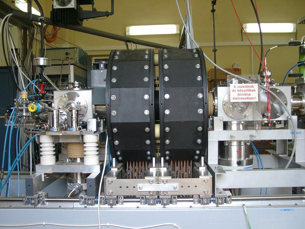
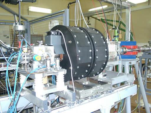
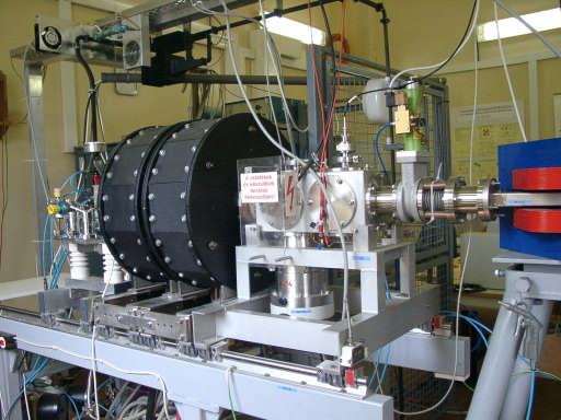
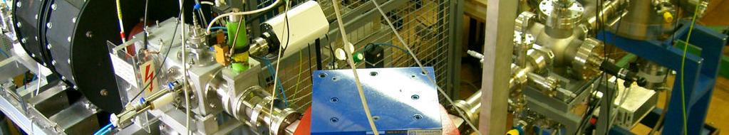
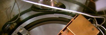
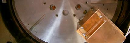
3 The ATOMKI-ECRIS 14.3 GHz/1 kw Axial field:1.2/0.4/1.0 T Radial al field: : 0.9 T Chamber: 58x200 Extraction: : KV 3


4 Two versions of the ECRIS ATOMKI-ECRIS-A ATOMKI-ECRIS-B Klystron, 14 GHz, 1000 W TWTAs, 6-18 GHz, 20 W Magnets: 1.2/0.4/1.0 and 0.9 T Magnets: 0.9/0.3/0.9 and 0.7 T Plasma chamber: 6x22 cm Plasma chamber: 10x40 cm! cm For HCI plasmas/beams For LCI, large-size plasmas 4

, no C60 research")
 Mixture plasmas (C60+X)")

5 1. Fullerene-based new materials (C60+X) to be produced in ECR-discharge Since 2000 fullerene plasmas and beams have been produced at the ATOMKI ECRIS C60: just a working material (as Ne, Ar, Fe), no C60 research Production of C60 ion beam (intensity, charge) Fullerene derivatives (destroyingadding) Mixture plasmas (C60+X) New materials (by C60+X) to detect in beam New materials to produce in macroscopic quantity Applications (surface coating, etc.) 5
6 Basic C60 experiments 6


 Quantum")


7 Slide made by R. Hatakeyama, Tohoku University, Sendai Next-Generation Information & Nano-Bio Technologies Devices ( energy / evaluation / semiconductor / storage / display / bio) Quantum computing Superconductivity High-efficient Small-sized Spintronics organic electronic circuit solar cell Gaseous Plasmas High-accuracy gene diagnosis High-density magnetic memory Low-power flat panel display High-sensitivity Bio sensor Creation of New-Functional Evolved-Nanomaterials Solution Plasmas Nanoscopic Plasma Processes Fullerene Nanotube Colloid Nanocarbon Network 7
 agent, magnetic nano-particle In ECR ion sources: Evaporation of C60 is solved (500 C) Production of fullerene derivatives is possible such")
 2.")
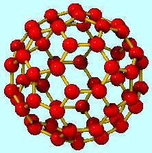
8 Iron encapsulated in fullerene Ha X=Fe Nanotechnology new SC materials quantum computing Medical tratments ultra-contrast Magnetic Resonance Imaging (MRI) agent, magnetic nano-particle In ECR ion sources: Evaporation of C60 is solved (500 C) Production of fullerene derivatives is possible such as (C60)+, (C58)+, (C56)+,, (C60)++, (C58)++, (C56)++,, Calculations showed that fullerene derivatives are less stable Therefore we must make a two-components plasma 1. component: C60 (mass and charge to be regulated) 2. component: Fe: pure iron gas, positive ions with optimal energy Synthesis: volume or surface? 8


9 Iron plasma in ECR ion sources (pre-experiments) Filament ovens: high temperature, large size, impurities Sputtering: high microwave power, high voltage, Sublimation: omly in chemical compounds, e.g. ferrocene Fe(C5H5)2: many non-wanted C, H, CxHx External ion source (e.g. MEVVA): complicated to connect (?) Indution oven: only iron! 9


10 It was decided to build a new ECR ion source at Toyo University, Kawagoe, Japan. To produce new, fullerene-based materials, mainly metal-encapsulated fullerenes. It is called: Bio-Nano-ECRIS Collaborators: Toyo Univ., NIRS, Osaka Univ., Tateyama Co. and ATOMKI 1st step: geometry and magnetic trap Hexapole: modified AECR-U ATOMKI-ECRIS-B 10
.")
11 The Bio-Nano-ECRIS project at Toyo University Geometry: plasma chamber OD=14 cm, L=35 cm. Microwave: 8-10 GHz, optional 2.45 GHz 2nd frequency. Mirror field: 2 identical RT-coils, max Tesla. Hexapole: NdFeB, modified AECRU design, 0.72/0.45 Tesla. Fullerene gas: using simple filament oven or evaporation boat. Iron gas: by induction oven (under development). Beamline: AM to transport upto 5 KV beams with M=800. First gas plasma: 2008 March Fe+C60 mixing: Induction oven, under development Bio-Nano-ECRIS, Toyo University,

 coating as intermediate layer between metal and organic tissue C60 ions can be shot to the metal surface with any required velocity: balls remain intact or damaged fullerene")
12 2. Bone cell growth on titanium coated with fullerene. ATOMKI ECRIS Group and Unideb Faculty of Dentistry collaboration Osseointegration : bone formation on Ti implants. Efforts: accelerate bone formation, improve lifetime and mechanical stability. Nanotechnology: new ways in implant technics Biological usefulness of Ti implants can be improved by (1) surface modification or (2) surface coating. Our idea: fullerene (C60) coating as intermediate layer between metal and organic tissue C60 ions can be shot to the metal surface with any required velocity: balls remain intact or damaged fullerene molecules are very reactive: hydroxyl etc other groups can be connected Such derivatised fullerenes are medically useful Physical part: to coat titanium surfaces by fullerenes with various velocity and thickness. Biological tests: growing bone cells on Ti+C60 12
 ATOMKI-ECRIS-B configuration Primary beamline, 50 cm distance from plasma 90% of")

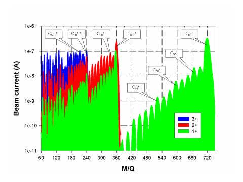
13 Task: irradiate simultaneously 10 Ti samples Size: 10x10x0.5 mm (d=50 mm beam is necessary) ATOMKI-ECRIS-B configuration Primary beamline, 50 cm distance from plasma 90% of the beam is single-charged 80% of the extracted beam is fullerene 90 deg beamline: just composition check U=250 V and U=500 V extraction voltages beam accuracy on 5 segments: less than 10% difference total intensity hit the samples: ena C60 thickness estimated: 1 and 5 layers 13
14 Summary of the Ti coatings by C60 Ti sample series C60 fraction in beam (%) Beam energy (ev) Number of C60 Time of molecular layers irradiation on the Ti surface (min)
 Cells dual labeled with special")
.")
15 Human embryonic bone cells were cultured onto the Ti substrates for 48 hours (type: palatal mesenchymal pre-osteoblast, HEPM 1486, ATCC) Cells dual labeled with special markers (FITC-falloidin), actine and vinculine Confocal imaging: laser scanning microscope (LSM 510, Carl Zeiss). Bone cells grown on glass Bone cells grown on Ti+C60 (250 ev) 15


 Further experiments: optimal")
16 The morphology of the cells is different compared to the control substrate The control cells on glass are quite spread showing an interconnected morphology The cells grown on the Ti substrates are more spindle-like shape showing denser actine and vinculine structure But there is no remarkable difference between the four Ti+C60 series, so far. Glass: Ti+C60: This first experiment: successful Proved: C60 coating does not prevent bone cells grows. High number of bone cells grew on Ti+C60 (~5*105/cm3) Further experiments: optimal beam properties (energy, rate, density, composition) Goal: improve physical (Ti-C60) and biological (C60-cells) properties 16


17 3. Modificaction of thin films by multiply charged ions : individual slow ions hitting the surface Amorphous Se layers, 500 nm, on mica Needle-like SbSJ crystals Xe charge Energy (KeV) Xe gas natural 1.0 Charge: 20+, 24+ Ion flux: ion/nm2 0.1 Epot Ekin (U=0.1) Ekin (U=2) Ekin (U=10) Ekin (U=0.5) Extraction voltage: U= 4 10 KV 17


18 Surface structuring AFM photos Xe E= kev Production of surface micro and nanostructures in one step without etching Hillocks! One possible mechanism of nano-hillock formation consists in the process, similar to the radiation-stimulated creation and diffusion of defects to the drains at the surface. 18
19 : volume effects Precedents Ion irradiation induced structural changes (H+, D+) As2S3, AsSe, Se % T,T,% Laser induced structural changes Ions: Neq+ (q=4...8) Ekin= 120 kev fixed Sample: AsSe layer on glass d=700 nm Penetration depth R= 200 nm Measured parameter: darkening (T/T0) depending on the charge nm,, nm T / T0 exp( ad ) exp( a1 R ) exp( a ( d R )) exp( a1 R ) const 19
20 nm T/T0 0.6 T/T nm fluence, ion/cm fluens, 10 ion/cm 1.1 Our experiment showed that (T/T0)sat is larger for the sample irradiated with Ne8+ ions than for the one irradiated with Ne4+ ions. R, rel. units Global optical property can be effected by the charge! charge state
21 4. Guiding of slow, highly charged ions through nano-capillaries Ions with few kev energy have been transmitted through capillaries of thin PET and SiO2 insulating foils There was significant transmission even if the capillaries were tilted by large angles, i.e., when there is no geometrical transparency for straight line trajectories. The initial charge state may be or may be not changed. Guiding Region Scattering Region Δα 10 µm Prospective applications: 100 nm - ion guiding, directing, focusing slow ion beams in nanoscale devices. - they might be used for irradiating single cells and writing on charge sensitive surfaces 21


,")
22 : ATOMKI-ECRIS-A Target: membranes of nanochanneled Al2O3, thickness 15 μm, honeycomb capillary diameters: nm to prevent charging up: 20 nm Nb layers Neon (6+, 7+), argon (8+, 9+) Extraction: 500 V Beam: two 1 mm diaphragms at 205 mm Beam current pa Detectors: FC, ion-spectrometer (channeltron), multi-channel-plate (MCP) 22
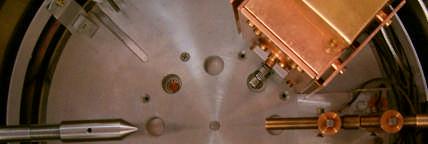
23 Spectrometer, MCP detector or Faraday cup Ion beam Capillary array Experimental setup 23
 10 100 Ne o 2+ Ne 5+ Ne Ne Ne 3+ 4+ 10 0.01 0.5 1 1.5 2 2.")
24 o 5 o 2.5 o o -5 Primary Beam Angular distributions at different tilt angles Target: 290 nm Al2O3 Normalized counts/s 1 6+ Ne Results 0.1 Sample: Al2O3, d=140 nm 1000 Tilt angle: 0 Intensity (arb. units) Ne o 2+ Ne 5+ Ne Ne Ne Ion energy/charge (kev) 1E Observation angle (degree) The capillary guiding works! UV photons were generated in the AM chamber Deflector+MCP can separate them Deflector plates + Ion CSD after the capilleries Sample Photons ~ mm Ion beam 24 3
25 Comparison and summary Project short name: Endohedral fullerenes Ti implants coating Thin layer modification Capillary guiding Ion source: ATOMKI-ECRIS-B ATOMKI-ECRIS-B ATOMKI-ECRIS-A ATOMKI-ECRIS-A and Bio-Nano-ECRIS Plasma/beam: Fe+, C60+ C60+ Ne4+ 8+ Ne6+,7+, Ar8+,9+ Beam diameter (mm) Microwave frequency (GHz) Microwave power (W) Synthesis in plasma or on surface Irradiation in the zero-degree beamline Beams with same total energy Puller on high negative voltage Extraction voltage (V) Specification: The tasks and beam requirements were different, but the ECR source proved to be versatile 25 enough to fulfill all these jobs and serves as a very useful multi-purpose facility.
26 Thank you for your attention! 26
APPLICATION OF THE ATOMKI-ECRIS FOR MATERIALS RESEARCH AND PROSPECTS OF THE MEDICAL UTILIZATION*
 APPLICATION OF THE ECRIS FOR MATERIALS RESEARCH AND PROSPECTS OF THE MEDICAL UTILIZATION* S. Biri #, I. Iván, Z. Juhász, B. Sulik, Institute of Nuclear Research (ATOMKI), Debrecen, Hungary Cs. Hegedűs,
Nano-ECRIS project: a new ECR ion source at Toyo University to produce endohedral fullerenes
 The Bio-Nano Nano-ECRIS project: a new ECR ion source at Toyo University to produce endohedral fullerenes ECRIS 2008 18th International Workshop on ECR Ion Sources Chicago, Illinois USA - September 15-18,
Studies of the ECR plasma in the visible light range
 Studies of the ECR plasma in the visible light range S. Biri, R. Rácz, J. Pálinkás* Institute of Nuclear Research (ATOMKI), Debrecen, Hungary *University of Debrecen, Dept. Exp. Physics, Hungary 1 S. Biri,
ACTA PHYSICA DEBRECENIENSIS XLI, 71 (2007) HEAVY ION PLASMAS AND HIGHLY CHARGED BEAMS. Abstract
 HEAVY ION PLASMAS AND HIGHLY CHARGED BEAMS. Abstract") ACTA PHYSICA DEBRECENIENSIS XLI, 71 (2007) HEAVY ION PLASMAS AND HIGHLY CHARGED BEAMS J. Pálinkás 1, E. Takács 1, S. Kökényesi 1, S. Biri 2, G. Szitási 1, I. Iván 2, É. Fekete 2, L.T. Hundson 3 1 University
ACTA PHYSICA DEBRECENIENSIS XLI, 71 (2007) HEAVY ION PLASMAS AND HIGHLY CHARGED BEAMS J. Pálinkás 1, E. Takács 1, S. Kökényesi 1, S. Biri 2, G. Szitási 1, I. Iván 2, É. Fekete 2, L.T. Hundson 3 1 University
Highly charged ion beams applied to fabrication of Nano-scale 3D structures. Sadao MOMOTA Kochi University of Technology
 Highly charged ion beams applied to fabrication of Nano-scale 3D structures Sadao MOMOTA Kochi University of Technology Introduction 1 Prospect of microscopic structures 2D Semiconductor 3D Ex. MEMS http://www.rise.waseda.ac.jp/proj/sci/s98s08/j-s98s08.html
ACTA PHYSICA DEBRECINA XLVIII, 1 (2014) MODIFICATION OF TITANIUM SURFACE BY GOLD ION BEAM. Abstract
 MODIFICATION OF TITANIUM SURFACE BY GOLD ION BEAM. Abstract") ACTA PHYSICA DEBRECINA XLVIII, 1 (2014) MODIFICATION OF TITANIUM SURFACE BY GOLD ION BEAM P. Hajdu 1, 2, S. Biri 1, R. Racz 1, S. Kökényesi 2, I. Csarnovics 2, A. Csik 1, K. Vad 1 1 Institute for Nuclear
ACTA PHYSICA DEBRECINA XLVIII, 1 (2014) MODIFICATION OF TITANIUM SURFACE BY GOLD ION BEAM P. Hajdu 1, 2, S. Biri 1, R. Racz 1, S. Kökényesi 2, I. Csarnovics 2, A. Csik 1, K. Vad 1 1 Institute for Nuclear
The accelerators at LNS - INFN and diagnostics aspects of the radioactive beams
 The accelerators at LNS - INFN and diagnostics aspects of the radioactive beams L. Cosentino, P. Finocchiaro, A. Pappalardo LNS INFN Catania J. Harasimowicz Univ. of Liverpool Cockroft Institute LNS INFN
Developments of the RCNP cyclotron cascade
 CYCLOTRONS 2007 The 18th International Conference on Cyclotrons and Their Applications Developments of the RCNP cyclotron cascade K. Hatanaka,, M. Fukuda, T. Saito, T. Yorita,, H. Tamura, M. Kibayashi,
Nova 600 NanoLab Dual beam Focused Ion Beam IITKanpur
 Nova 600 NanoLab Dual beam Focused Ion Beam system @ IITKanpur Dual Beam Nova 600 Nano Lab From FEI company (Dual Beam = SEM + FIB) SEM: The Electron Beam for SEM Field Emission Electron Gun Energy : 500
RECENT DEVELOPMENTS AND ELECTRON DENSITY SIMULATIONS AT THE ATOMKI 14.5 GHz ECRIS
 RECENT DEVELOPMENTS AND ELECTRON DENSITY SIMULATIONS AT THE ATOMKI 14.5 GHz ECRIS S. Biri 1#, R. Rácz 1,, Z. Perduk 1, I. Vajda 1 and J. Pálinkás 2 1 Institute of Nuclear Research (ATOMKI), Hungary, H-4026
MIDAS-NA: MInimization of Destructive plasma processes in ECR ion source
 MIDAS-NA: MInimization of Destructive plasma processes in ECR ion source H. Koivisto, ENSAR Town Meeting, 17-19 th April 2018, Groningen, The Netherlands Partners: JYFL ATOMKI CERN GANIL GSI KVI LPSC UCLM
Gaetano L Episcopo. Scanning Electron Microscopy Focus Ion Beam and. Pulsed Plasma Deposition
 Gaetano L Episcopo Scanning Electron Microscopy Focus Ion Beam and Pulsed Plasma Deposition Hystorical background Scientific discoveries 1897: J. Thomson discovers the electron. 1924: L. de Broglie propose
A DIVISION OF ULVAC-PHI
 A DIVISION OF ULVAC-PHI X-ray photoelectron spectroscopy (XPS/ESCA) is the most widely used surface analysis technique and has many well established industrial and research applications. XPS provides
Ion Beam Cocktail Development and ECR Ion Source Plasma Physics Experiments at JYFL
 Ion Beam Cocktail Development and ECR Ion Source Plasma Physics Experiments at JYFL Olli Tarvainen 11th International Conference on Heavy Ion Accelerator Technology Venice, Italy 8-12 June 29 Outline JYFL
Accelerated Neutral Atom Beam (ANAB)
") Accelerated Neutral Atom Beam (ANAB) Development and Commercialization July 2015 1 Technological Progression Sometimes it is necessary to develop a completely new tool or enabling technology to meet future
Accelerated Neutral Atom Beam (ANAB) Development and Commercialization July 2015 1 Technological Progression Sometimes it is necessary to develop a completely new tool or enabling technology to meet future
Experiments with biased side electrodes in electron cyclotron resonance ion sources a)
") Experiments with biased side electrodes in electron cyclotron resonance ion sources a) A. G. Drentje, 1,b) A. Kitagawa, 1 T. Uchida, 2 R. Rácz, 3 and S. Biri 3 1 National Institute of Radiological Sciences
Experiments with biased side electrodes in electron cyclotron resonance ion sources a) A. G. Drentje, 1,b) A. Kitagawa, 1 T. Uchida, 2 R. Rácz, 3 and S. Biri 3 1 National Institute of Radiological Sciences
Auger Electron Spectroscopy Overview
 Auger Electron Spectroscopy Overview Also known as: AES, Auger, SAM 1 Auger Electron Spectroscopy E KLL = E K - E L - E L AES Spectra of Cu EdN(E)/dE Auger Electron E N(E) x 5 E KLL Cu MNN Cu LMM E f E
6.5 Optical-Coating-Deposition Technologies
 92 Chapter 6 6.5 Optical-Coating-Deposition Technologies The coating process takes place in an evaporation chamber with a fully controlled system for the specified requirements. Typical systems are depicted
The heavy ion irradiation facility at KVI-CART
 The heavy ion irradiation facility at KVI-CART Brian N. Jones 1, Marc-Jan van Goethem 1,2, Rob Kremers 1, Harry Kiewiet 1, Emiel van der Graaf 1, Sytze Brandenburg 1 1 University of Groningen, KVI-Center
Coulomb crystal extraction from an ion trap for application to nano-beam source"
 Coulomb crystal extraction from an ion trap for application to nano-beam source" K. Ito, K. Izawa, H. Higaki and H. Okamoto,! Aadvanced Sciences of Matter, Hiroshima University,! 1-3-1 Kagamiyama, Higashi-Hiroshima,
Chapter 10. Nanometrology. Oxford University Press All rights reserved.
 Chapter 10 Nanometrology Oxford University Press 2013. All rights reserved. 1 Introduction Nanometrology is the science of measurement at the nanoscale level. Figure illustrates where nanoscale stands
MSN551 LITHOGRAPHY II
 MSN551 Introduction to Micro and Nano Fabrication LITHOGRAPHY II E-Beam, Focused Ion Beam and Soft Lithography Why need electron beam lithography? Smaller features are required By electronics industry:
Fadei Komarov Alexander Kamyshan
 Fadei Komarov Alexander Kamyshan Institute of Applied Physics Problems, Belarusian State University, Minsk, Belarus KomarovF@bsu.by Tasks and Objects 2 Introduction and motivation Experimental setup designed
THIN FILMS FOR PHOTOVOLTAICS AND OTHER APPLICATIONS. BY Dr.A.K.SAXENA PHOTONICS DIVISION INDIAN INSTITUTE OF ASTROPHYSICS
 THIN FILMS FOR PHOTOVOLTAICS AND OTHER APPLICATIONS BY Dr.A.K.SAXENA PHOTONICS DIVISION INDIAN INSTITUTE OF ASTROPHYSICS BACKGROUND 2.8 meter coating plant at VBO, Kavalur 1.5 meter coating plant at VBO,
Chapter 12. Nanometrology. Oxford University Press All rights reserved.
 Chapter 12 Nanometrology Introduction Nanometrology is the science of measurement at the nanoscale level. Figure illustrates where nanoscale stands in relation to a meter and sub divisions of meter. Nanometrology
Opportunities for Advanced Plasma and Materials Research in National Security
 Opportunities for Advanced Plasma and Materials Research in National Security Prof. J.P. Allain allain@purdue.edu School of Nuclear Engineering Purdue University Outline: Plasma and Materials Research
TMT4320 Nanomaterials November 10 th, Thin films by physical/chemical methods (From chapter 24 and 25)
") 1 TMT4320 Nanomaterials November 10 th, 2015 Thin films by physical/chemical methods (From chapter 24 and 25) 2 Thin films by physical/chemical methods Vapor-phase growth (compared to liquid-phase growth)
1 TMT4320 Nanomaterials November 10 th, 2015 Thin films by physical/chemical methods (From chapter 24 and 25) 2 Thin films by physical/chemical methods Vapor-phase growth (compared to liquid-phase growth)
Accelerated Neutral Atom Beam Processing of Ultra-thin Membranes to Enhance EUV Transmittance. February 22, 2015
 Accelerated Neutral Atom Beam Processing of Ultra-thin Membranes to Enhance EUV Transmittance February 22, 2015 1 Participation / Contacts Exogenesis Corporation, ANAB Technology Sean Kirkpatrick, Son
Preliminary Simulation of Beam Extraction for the 28 GHz ECR Ion Source
 Preliminary Simulation of Beam Extraction for the 28 GHz ECR Ion Source Bum-Sik Park*, Yonghwan Kim and Seokjin Choi RISP, Institute for Basic Science, Daejeon 305-811, Korea The 28 GHz ECR(Electron Cyclotron
Secondary ion mass spectrometry (SIMS)
") Secondary ion mass spectrometry (SIMS) ELEC-L3211 Postgraduate Course in Micro and Nanosciences Department of Micro and Nanosciences Personal motivation and experience on SIMS Offers the possibility to
Secondary ion mass spectrometry (SIMS) ELEC-L3211 Postgraduate Course in Micro and Nanosciences Department of Micro and Nanosciences Personal motivation and experience on SIMS Offers the possibility to
Nanotechnology Fabrication Methods.
 Nanotechnology Fabrication Methods. 10 / 05 / 2016 1 Summary: 1.Introduction to Nanotechnology:...3 2.Nanotechnology Fabrication Methods:...5 2.1.Top-down Methods:...7 2.2.Bottom-up Methods:...16 3.Conclusions:...19
Supplementary Figure 1 Detailed illustration on the fabrication process of templatestripped
 Supplementary Figure 1 Detailed illustration on the fabrication process of templatestripped gold substrate. (a) Spin coating of hydrogen silsesquioxane (HSQ) resist onto the silicon substrate with a thickness
The scanning microbeam PIXE analysis facility at NIRS
 Nuclear Instruments and Methods in Physics Research B 210 (2003) 42 47 www.elsevier.com/locate/nimb The scanning microbeam PIXE analysis facility at NIRS Hitoshi Imaseki a, *, Masae Yukawa a, Frank Watt
Single ion implantation for nanoelectronics and the application to biological systems. Iwao Ohdomari Waseda University Tokyo, Japan
 Single ion implantation for nanoelectronics and the application to biological systems Iwao Ohdomari Waseda University Tokyo, Japan Contents 1.History of single ion implantation (SII) 2.Novel applications
COST MP0601 Short Wavelength Laboratory Sources
 Background: Short wavelength radiation has been used in medicine and materials studies since immediately after the 1895 discovery of X-rays. The development of synchrotron sources over the last ~25 years
188 L. Jakubowski and M.J. Sadowski temperature. Some examples of the registered X-ray images are shown in Fig.1. Figure 1. X-ray pinhole images from
 Brazilian Journal of Physics, vol. 32, no. 1, March, 2002 187 Hot-Spots in Plasma-Focus Discharges as Intense Sources of Different Radiation Pulses L. Jakubowski and M.J. Sadowski The Andrzej Soltan Institute
2008,, Jan 7 All-Paid US-Japan Winter School on New Functionalities in Glass. Controlling Light with Nonlinear Optical Glasses and Plasmonic Glasses
 2008,, Jan 7 All-Paid US-Japan Winter School on New Functionalities in Glass Photonic Glass Controlling Light with Nonlinear Optical Glasses and Plasmonic Glasses Takumi FUJIWARA Tohoku University Department
Plasma Deposition (Overview) Lecture 1
 Lecture 1") Plasma Deposition (Overview) Lecture 1 Material Processes Plasma Processing Plasma-assisted Deposition Implantation Surface Modification Development of Plasma-based processing Microelectronics needs (fabrication
Plasma Deposition (Overview) Lecture 1 Material Processes Plasma Processing Plasma-assisted Deposition Implantation Surface Modification Development of Plasma-based processing Microelectronics needs (fabrication
Crystalline Surfaces for Laser Metrology
 Crystalline Surfaces for Laser Metrology A.V. Latyshev, Institute of Semiconductor Physics SB RAS, Novosibirsk, Russia Abstract: The number of methodological recommendations has been pronounced to describe
Magnetic measurements (Pt. IV) advanced probes
 advanced probes") Magnetic measurements (Pt. IV) advanced probes Ruslan Prozorov October 2018 Physics 590B types of local probes microscopic (site-specific) NMR neutrons Mossbauer stationary Bitter decoration magneto-optics
Magnetic measurements (Pt. IV) advanced probes Ruslan Prozorov October 2018 Physics 590B types of local probes microscopic (site-specific) NMR neutrons Mossbauer stationary Bitter decoration magneto-optics
Secondary Ion Mass Spectrometry (SIMS)
") CHEM53200: Lecture 10 Secondary Ion Mass Spectrometry (SIMS) Major reference: Surface Analysis Edited by J. C. Vickerman (1997). 1 Primary particles may be: Secondary particles can be e s, neutral species
CHEM53200: Lecture 10 Secondary Ion Mass Spectrometry (SIMS) Major reference: Surface Analysis Edited by J. C. Vickerman (1997). 1 Primary particles may be: Secondary particles can be e s, neutral species
PHI 5000 Versaprobe-II Focus X-ray Photo-electron Spectroscopy
 PHI 5000 Versaprobe-II Focus X-ray Photo-electron Spectroscopy The very basic theory of XPS XPS theroy Surface Analysis Ultra High Vacuum (UHV) XPS Theory XPS = X-ray Photo-electron Spectroscopy X-ray
Keywords. 1=magnetron sputtering, 2= rotatable cathodes, 3=substrate temperature, 4=anode. Abstract
 Managing Anode Effects and Substrate Heating from Rotatable Sputter Targets. F. Papa*, V. Bellido-Gonzalez**, Alex Azzopardi**, Dr. Dermot Monaghan**, *Gencoa Technical & Business Support in US, Davis,
Supporting Information s for
 Supporting Information s for # Self-assembling of DNA-templated Au Nanoparticles into Nanowires and their enhanced SERS and Catalytic Applications Subrata Kundu* and M. Jayachandran Electrochemical Materials
Methods of surface analysis
 Methods of surface analysis Nanomaterials characterisation I RNDr. Věra Vodičková, PhD. Surface of solid matter: last monoatomic layer + absorbed monolayer physical properties are effected (crystal lattice
Infrastructure of Thin Films Laboratory in Institute of Molecular Physics Polish Academy of Sciences
 Infrastructure of Thin Films Laboratory in Institute of Molecular Physics Polish Academy of Sciences Outline Sample preparation Magnetron sputtering Ion-beam sputtering Pulsed laser deposition Electron-beam
Energetic particles and their detection in situ (particle detectors) Part II. George Gloeckler
 Part II. George Gloeckler") Energetic particles and their detection in situ (particle detectors) Part II George Gloeckler University of Michigan, Ann Arbor, MI University of Maryland, College Park, MD Simple particle detectors Gas-filled
Energetic particles and their detection in situ (particle detectors) Part II George Gloeckler University of Michigan, Ann Arbor, MI University of Maryland, College Park, MD Simple particle detectors Gas-filled
Magnetic measurements (Pt. IV) advanced probes
 advanced probes") Magnetic measurements (Pt. IV) advanced probes Ruslan Prozorov 26 February 2014 Physics 590B types of local probes microscopic (site-specific) NMR neutrons Mossbauer stationary Bitter decoration magneto-optics
Magnetic measurements (Pt. IV) advanced probes Ruslan Prozorov 26 February 2014 Physics 590B types of local probes microscopic (site-specific) NMR neutrons Mossbauer stationary Bitter decoration magneto-optics
Chapter 6. Summary and Conclusions
 Chapter 6 Summary and Conclusions Plasma deposited amorphous hydrogenated carbon films (a-c:h) still attract a lot of interest due to their extraordinary properties. Depending on the deposition conditions
Ion Implantation. alternative to diffusion for the introduction of dopants essentially a physical process, rather than chemical advantages:
 Ion Implantation alternative to diffusion for the introduction of dopants essentially a physical process, rather than chemical advantages: mass separation allows wide varies of dopants dose control: diffusion
Dielectric Meta-Reflectarray for Broadband Linear Polarization Conversion and Optical Vortex Generation
 Supporting Information Dielectric Meta-Reflectarray for Broadband Linear Polarization Conversion and Optical Vortex Generation Yuanmu Yang, Wenyi Wang, Parikshit Moitra, Ivan I. Kravchenko, Dayrl P. Briggs,
Bremsstrahlung and Ion Beam Current Measurements with SuSI ECR Ion Source
 Bremsstrahlung and Ion Beam Current Measurements with SuSI ECR Ion Source Tommi Ropponen NSCL/MSU East Lansing, MI, USA ropponen@nscl.msu.edu August 25 th 20, ECRIS, Grenoble, France T. Ropponen, ECRIS,
Ionization Techniques Part IV
 Ionization Techniques Part IV CU- Boulder CHEM 5181 Mass Spectrometry & Chromatography Presented by Prof. Jose L. Jimenez High Vacuum MS Interpretation Lectures Sample Inlet Ion Source Mass Analyzer Detector
INTRODUCTION TO THE HYBRID PLASMA EQUIPMENT MODEL
 INTRODUCTION TO THE HYBRID PLASMA EQUIPMENT MODEL Prof. Mark J. Kushner Department of Electrical and Computer Engineering 1406 W. Green St. Urbana, IL 61801 217-144-5137 mjk@uiuc.edu http://uigelz.ece.uiuc.edu
Imaging Methods: Scanning Force Microscopy (SFM / AFM)
") Imaging Methods: Scanning Force Microscopy (SFM / AFM) The atomic force microscope (AFM) probes the surface of a sample with a sharp tip, a couple of microns long and often less than 100 Å in diameter.
Imaging Methods: Scanning Force Microscopy (SFM / AFM) The atomic force microscope (AFM) probes the surface of a sample with a sharp tip, a couple of microns long and often less than 100 Å in diameter.
Nanotechnology Nanofabrication of Functional Materials. Marin Alexe Max Planck Institute of Microstructure Physics, Halle - Germany
 Nanotechnology Nanofabrication of Functional Materials Marin Alexe Max Planck Institute of Microstructure Physics, Halle - Germany Contents Part I History and background to nanotechnology Nanoworld Nanoelectronics
RCNP cyclotron facility
 11th International Conference on HEAVY ION ACCELERATOR TECHNOLOGY RCNP cyclotron facility K. Hatanaka hatanaka@rcnp.osaka-u.ac.jp Research Center for Nuclear Physics Osaka University HIAT09 TU9 June 9,
Fabrication Methods: Chapter 4. Often two methods are typical. Top Down Bottom up. Begins with atoms or molecules. Begins with bulk materials
 Fabrication Methods: Chapter 4 Often two methods are typical Top Down Bottom up Begins with bulk materials Begins with atoms or molecules Reduced in size to nano By thermal, physical Chemical, electrochemical
The electron accelerator of the ISOF-CNR Institute: its characteristics and use
 The electron accelerator of the ISOF-CNR Institute: its characteristics and use P. Fuochi, U. Corda, and M. Lavalle ISOF-CNR Institute, Via P. Gobetti 101, I-40129 Bologna, Italy LINAC Laboratory: ISOF-CNR,
Industrial Applications of Ultrafast Lasers: From Photomask Repair to Device Physics
 Industrial Applications of Ultrafast Lasers: From Photomask Repair to Device Physics Richard Haight IBM TJ Watson Research Center PO Box 218 Yorktown Hts., NY 10598 Collaborators Al Wagner Pete Longo Daeyoung
Auger Electron Spectroscopy
 Auger Electron Spectroscopy Auger Electron Spectroscopy is an analytical technique that provides compositional information on the top few monolayers of material. Detect all elements above He Detection
Superconducting Single-photon Detectors
 : Quantum Cryptography Superconducting Single-photon Detectors Hiroyuki Shibata Abstract This article describes the fabrication and properties of a single-photon detector made of a superconducting NbN
Supporting Information
 Supporting Information Clustered Ribbed-Nanoneedle Structured Copper Surfaces with High- Efficiency Dropwise Condensation Heat Transfer Performance Jie Zhu, Yuting Luo, Jian Tian, Juan Li and Xuefeng Gao*
MEASUREMENT OF TEMPORAL RESOLUTION AND DETECTION EFFICIENCY OF X-RAY STREAK CAMERA BY SINGLE PHOTON IMAGES
 Proceedings of IBIC212, Tsukuba, Japan MEASUREMENT OF TEMPORAL RESOLUTION AND DETECTION EFFICIENCY OF X-RAY STREAK CAMERA BY SINGLE PHOTON IMAGES A. Mochihashi, M. Masaki, S. Takano, K. Tamura, H. Ohkuma,
David B. Cassidy. Department of Physics and Astronomy, University of California, Riverside, USA. Varenna, July 09
 Experimental production of many- positron systems: L2, techniques David B. Cassidy Department of Physics and Astronomy, University of California, Riverside, USA cassidy@physics.ucr.edu Varenna, July 09
Performance of the ANL ECR Charge Breeder. with Low Mass Beams. Investigations with low mass species. Review of charge breeder design
 Review of charge breeder design Investigations with low mass species Injection simulations Richard Vondrasek, Sergey Kutsaev, Richard Pardo, Robert Scott Argonne National Laboratory Pierre Delahaye, Laurent
Imaging Carbon materials with correlative Raman-SEM microscopy. Introduction. Raman, SEM and FIB within one chamber. Diamond.
 Imaging Carbon materials with correlative Raman-SEM microscopy Application Example Carbon materials are widely used in many industries for their exceptional properties. Electric conductance, light weight,
Introductory Lecture on Plasmas EEG 783. Robert A. Schill, Jr. University of Nevada Las Vegas
 Introductory Lecture on Plasmas EEG 783 Robert A. Schill, Jr. University of Nevada Las Vegas States of Matter Four Naturally Occurring States of Matter Solids, Liquids, Gas, Plasmas Solids Condense matter
object objective lens eyepiece lens
 Advancing Physics G495 June 2015 SET #1 ANSWERS Field and Particle Pictures Seeing with electrons The compound optical microscope Q1. Before attempting this question it may be helpful to review ray diagram
Preparation of Nanostructures(Příprava Nanostruktur)
") Preparation of Nanostructures (Příprava Nanostruktur) jaroslav.hamrle@vsb.cz September 23, 2013 Outline 1 Introduction 2 Bulk crystal growth 3 Thin film preparation 4 Lateral structures 5 Surface plasma
Preparation of Nanostructures (Příprava Nanostruktur) jaroslav.hamrle@vsb.cz September 23, 2013 Outline 1 Introduction 2 Bulk crystal growth 3 Thin film preparation 4 Lateral structures 5 Surface plasma
For use with Comprehensive Secondary Physics
 SUB- 166 SUB- 167 For use with Physics Secondary Form Four Physics : Term One SUB- 1 Converging and diverging lenses diverging and converging lenses. Using light beams to distinguish between diverging
Tailoring of optical properties of LiNbO 3 by ion implantation
 SMR/1758-14 "Workshop on Ion Beam Studies of Nanomaterials: Synthesis, Modification and Characterization" 26 June - 1 July 2006 Tailoring of Optical Properties of LiNbO3 by ion implantation Cinzia SADA
From nanophysics research labs to cell phones. Dr. András Halbritter Department of Physics associate professor
 From nanophysics research labs to cell phones Dr. András Halbritter Department of Physics associate professor Curriculum Vitae Birth: 1976. High-school graduation: 1994. Master degree: 1999. PhD: 2003.
Self-assembled nanostructures for antireflection optical coatings
 Self-assembled nanostructures for antireflection optical coatings Yang Zhao 1, Guangzhao Mao 2, and Jinsong Wang 1 1. Deaprtment of Electrical and Computer Engineering 2. Departmentof Chemical Engineering
A DIVISION OF ULVAC-PHI. Quantera II. Scanning XPS Microprobe
 A DIVISION OF ULVAC-PHI Quantera II Scanning XPS Microprobe X-ray Photoelectron Spectroscopy (XPS/ESCA) is the most widely used surface analysis technique and has many well established industrial and
M. Audronis 1 and F. Zimone 2 1. Nova Fabrica Ltd. 1. Angstrom Sciences Inc.
 M. Audronis 1 and F. Zimone 2 1 Nova Fabrica Ltd. 1 Angstrom Sciences Inc. Email: info@novafabrica.biz 1 Founded in 2013 the company is based in Lithuania (northern EU). NF are involved in two business
Introduction to Thin Film Processing
 Introduction to Thin Film Processing Deposition Methods Many diverse techniques available Typically based on three different methods for providing a flux of atomic or molecular material Evaporation Sputtering
Quantum Technologies CCEM Workshop March 23 rd, 2017
 Quantum Technologies CCEM Workshop March 23 rd, 2017 JT Janssen Welcome to the National Physical Laboratory The first quantum revolution h V n f 2 e 1 The second quantum revolution Superposition Entanglement
New Tandetron Accelerator Laboratory at MTA Atomki, Debrecen: Multi-Purpose and Multi-User Facility
 New Tandetron Accelerator Laboratory at MTA Atomki, Debrecen: Multi-Purpose and Multi-User Facility István Rajta MTA Atomki, Debrecen, Hungary Dirk Mous High Voltage Engineering Europa B.V., Amersfoort,
Carbon Nanotube Thin-Films & Nanoparticle Assembly
 Nanodevices using Nanomaterials : Carbon Nanotube Thin-Films & Nanoparticle Assembly Seung-Beck Lee Division of Electronics and Computer Engineering & Department of Nanotechnology, Hanyang University,
X-Ray Photoelectron Spectroscopy (XPS) Prof. Paul K. Chu
 Prof. Paul K. Chu") X-Ray Photoelectron Spectroscopy (XPS) Prof. Paul K. Chu X-ray Photoelectron Spectroscopy Introduction Qualitative analysis Quantitative analysis Charging compensation Small area analysis and XPS imaging
X-Ray Photoelectron Spectroscopy (XPS) Prof. Paul K. Chu X-ray Photoelectron Spectroscopy Introduction Qualitative analysis Quantitative analysis Charging compensation Small area analysis and XPS imaging
HIRFL STATUS AND HIRFL-CSR PROJECT IN LANZHOU
 HIRFL STATUS AND HIRFL-CSR PROJECT IN LANZHOU J. W. Xia, Y. F. Wang, Y. N. Rao, Y. J. Yuan, M. T. Song, W. Z. Zhang, P. Yuan, W. Gu, X. T. Yang, X. D. Yang, S. L. Liu, H.W.Zhao, J.Y.Tang, W. L. Zhan, B.
Characterization of Secondary Emission Materials for Micro-Channel Plates. S. Jokela, I. Veryovkin, A. Zinovev
 Characterization of Secondary Emission Materials for Micro-Channel Plates S. Jokela, I. Veryovkin, A. Zinovev Secondary Electron Yield Testing Technique We have incorporated XPS, UPS, Ar-ion sputtering,
Experimental High Energy Physics & Plasma Etching
 Experimental High Energy Physics & Plasma Etching Samah M. Balouza Purdue University Nikhef Doctoral Interview 07/06/2017 Outlines Plasma Physics Research Experimental High Energy PhysicsResearch Samah
Dual Beam Helios Nanolab 600 and 650
 Dual Beam Helios Nanolab 600 and 650 In the Clean Room facilities of the INA LMA, several lithography facilities permit to pattern structures at the micro and nano meter scale and to create devices. In
Defense Technical Information Center Compilation Part Notice
 UNCLASSIFIED Defense Technical Information Center Compilation Part Notice ADP013065 TITLE: Two-Dimensional Photonic Crystal Fabrication Using Fullerene Films DISTRIBUTION: Approved for public release,
Formation of High-b ECH Plasma and Inward Particle Diffusion in RT-1
 J Fusion Energ (2010) 29:553 557 DOI 10.1007/s10894-010-9327-6 ORIGINAL RESEARCH Formation of High-b ECH Plasma and Inward Particle Diffusion in RT-1 H. Saitoh Z. Yoshida J. Morikawa Y. Yano T. Mizushima
Applications of Micro-Area Analysis Used by JPS-9200 X-ray Photoelectron Spectrometer
 Applications of Micro-Area Analysis Used by JPS-9200 X-ray Photoelectron Spectrometer Yoshitoki Iijima Application & Research Center, JEOL Ltd. Introduction Recently, with advances in the development of
LECTURE 11 ELECTROMAGNETIC WAVES & POLARIZATION. Instructor: Kazumi Tolich
 LECTURE 11 ELECTROMAGNETIC WAVES & POLARIZATION Instructor: Kazumi Tolich Lecture 11 2 25.5 Electromagnetic waves Induced fields Properties of electromagnetic waves Polarization Energy of electromagnetic
Secondary Ion Mass Spectrometry (SIMS) Thomas Sky
 Thomas Sky") 1 Secondary Ion Mass Spectrometry (SIMS) Thomas Sky Depth (µm) 2 Characterization of solar cells 0,0 1E16 1E17 1E18 1E19 1E20 0,2 0,4 0,6 0,8 1,0 1,2 P Concentration (cm -3 ) Characterization Optimization
1 Secondary Ion Mass Spectrometry (SIMS) Thomas Sky Depth (µm) 2 Characterization of solar cells 0,0 1E16 1E17 1E18 1E19 1E20 0,2 0,4 0,6 0,8 1,0 1,2 P Concentration (cm -3 ) Characterization Optimization
GEM: A new concept for electron amplification in gas detectors
 GEM: A new concept for electron amplification in gas detectors F. Sauli, Nucl. Instr. & Methods in Physics Research A 386 (1997) 531-534 Contents 1. Introduction 2. Two-step amplification: MWPC combined
CYCLOTRON-RESONANCE ION SOURCE (ECRIS) FOR THE PRODUCTION OF MULTIPLY CHARGED IONS
 FOR THE PRODUCTION OF MULTIPLY CHARGED IONS") CYCLOTRON-RESONANCE ION SOURCE (ECRIS) FOR THE PRODUCTION OF MULTIPLY CHARGED IONS M. Schlapp'*], R. Trassl[+', P. Hathirammi[*], R. W. McCullough"], J.B Greenwood[#] and E. Salzborn'+] ['I Argonne National
CYCLOTRON-RESONANCE ION SOURCE (ECRIS) FOR THE PRODUCTION OF MULTIPLY CHARGED IONS M. Schlapp'*], R. Trassl[+', P. Hathirammi[*], R. W. McCullough"], J.B Greenwood[#] and E. Salzborn'+] ['I Argonne National
Soft X-ray multilayer mirrors by ion assisted sputter deposition
 Soft X-ray multilayer mirrors by ion assisted sputter deposition Valentino Rigato INFN Laboratori Nazionali di Legnaro Bologna, September 21, 2010 Source: INFN-LNL-2009 V. RIGATO 1 SIF- Bologna September
Nanostructures induced by highly charged ions
 Nanostructures induced by highly charged ions R. Heller, R. Wilhelm, A. S. ElSaid, S. Facsko Institute for Ion Beam Physics and Materials Research in cooperation with: group of F. Aumayr: W. Meissl, G.
Laser and Plasma-based Nanotechnologies
 Simpozionul: De la excelenta la competitivitate: tehnologiile generice esentiale Aula Academiei Romane, Bucuresti 15 mai 2014. Laser and Plasma-based Nanotechnologies Marian ZAMFIRESCU National Institute
HIGH INTENSITY ION BEAMS AT GANIL F. Chautard, September 6th, Cyclotron 2010 Lanzhou, China, september F. Chautard
 HIGH INTENSITY ION BEAMS AT GANIL F. Chautard, September 6th, 2010 OUTLINE Operation modes at GANIL Statistics Stable beams Exotic beams ISOL In Flight Beam developments Stable beams Exotic beams Machine
X-Rays From Laser Plasmas
 X-Rays From Laser Plasmas Generation and Applications I. C. E. TURCU CLRC Rutherford Appleton Laboratory, UK and J. B. DANCE JOHN WILEY & SONS Chichester New York Weinheim Brisbane Singapore Toronto Contents
Progress in April December 2007 Schedule in Jan. March 2008
 A Report to the Advisory Committee of CNS The Accelerator Group Outline Upgrade of AVF Cyclotron Progress in April December 2007 Schedule in Jan. March 2008 Shigeru Kubono, Yukimitsu Ohshiro, Shin-ichi
University of Groningen. Extraction and transport of ion beams from an ECR ion source Saminathan, Suresh
 University of Groningen Extraction and transport of ion beams from an ECR ion source Saminathan, Suresh IMPORTANT NOTE: You are advised to consult the publisher's version (publisher's PDF) if you wish
Fluctuation Suppression during the ECH Induced Potential Formation in the Tandem Mirror GAMMA 10
 EXC/P8-2 Fluctuation Suppression during the ECH Induced Potential Formation in the Tandem Mirror GAMMA M. Yoshikawa ), Y. Miyata ), M. Mizuguchi ), Y. Oono ), F. Yaguchi ), M. Ichimura ), T. Imai ), T.