A DIVISION OF ULVAC-PHI. Quantera II. Scanning XPS Microprobe
|
|
|
- Mark Lloyd
- 5 years ago
- Views:
Transcription

1 A DIVISION OF ULVAC-PHI Quantera II Scanning XPS Microprobe


2
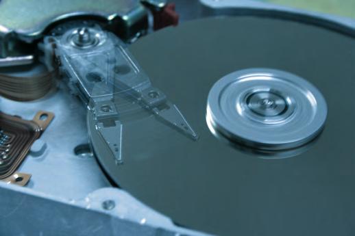
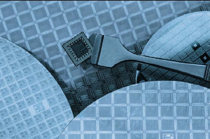
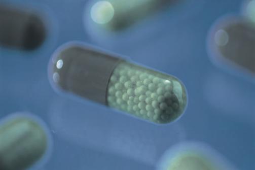
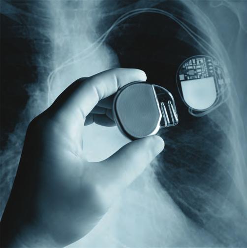
3 X-ray Photoelectron Spectroscopy (XPS/ESCA) is the most widely used surface analysis technique and has many well established industrial and research applications. XPS provides quantitative elemental and chemical state information from surfaces and thin film structures. XPS is applied to a diverse range of materials applications including: polymers, metals, catalysts, thin films, photovoltaics, batteries, wear coatings, nanomaterials, semiconductor devices, magnetic storage media, display technology, and biomedical devices. The Quantera II is built upon Physical Electronics (PHI) revolutionary scanning XPS microprobe instrument platform that includes: a patented micro-focused scanning x-ray source, patented dual beam charge neutralization technology, a floating column ion gun for optimized XPS sputter depth profiling, flexible robotic sample handling, and a fully automated internet ready instrument platform. The Quantera II increases the performance and productivity of these revolutionary technologies, providing the highest performance XPS system available to meet your current and future XPS needs.
 generated by scanning a focused 10 μm x-ray beam across the sample.")

4 THE SCANNING XPS MICROPROBE ADVANTAGE Quartz Crystal Monochromator Energy Analyzer Raster Scanned Electron Gun Unique Capabilities PHI s scanning XPS microprobe instrument platform provides secondary electron images (SXI) generated by scanning a focused 10 μm x-ray beam across the sample. These SXI images have a contrast mechanism that is dominated by photoelectron yield (composition), and therefore often reveal features that are not visible optically or related to topography. SXI images provide a high degree of confidence in locating small features for analysis. The micro-focused x-ray beam defines the analysis area pattern for large area spectroscopy, micro area spectroscopy, chemical state imaging, and depth profiling. Analyzer Input Lens Multi-Channel Detector Sample Al Anode PHI s patented scanning XPS microprobe technology delivers a micro-focused, raster scanned, monochromatic x-ray beam to the sample surface providing unique and powerful capabilities to our users.
 from a polymer")


5 SXI Multi-Area Spectroscopy MICRO AREA XPS Microprobe Workflow X-ray beam induced secondary electron image (SXI) from a polymer film reveals the presence of unexpected contaminants on the samples surface. Micro area spectra reveal the composition of the unknown contaminants. Chemical Imaging Elemental images show the smaller features in the secondary electron image do not contain fluorine. A micro area spectrum from the smaller features, obtained using a 10 μm diameter x-ray beam, identifies the presence of a second contaminant that contains Zn. A x-ray beam induced secondary electron image immediately revealed the presence of unexpected localized contaminants on a polymers surface. Micro area spectra obtained with a 20 μm diameter x-ray beam identified a fluorocarbon contaminant in a few minutes. Elemental maps show the smaller features in the secondary electron image do not contain fluorine. A micro area spectrum from the smaller features, obtained using a 10 μm diameter x-ray beam, identifies the presence of a second contaminant that contains Zn.

6 ROBUST AUTO ANALYSIS High Productivity Whether you are analyzing a thin polymer sheet, a large plastic lens, a steel razor blade, or electrically isolated solder bumps; the instrument set-up is the same. Point and click at an optical image to select the analysis areas. Then start the analysis with the dual beam neutralizer and the auto-z functions activated to provide automatic sample alignment and charge neutralization. There is no individual sample tuning, no concerns over sample composition and size, and no worries about walking away from the instrument and letting it automatically collect data from all your samples. No Special Sample Mounting or Masking Robust Automatic Sample Alignment ( Auto-Z ) Hands-Off Charge Neutralization


7 THIN FILM ANALYSIS Optimized Configuration 2 kev Ar sputter depth profile of the 10 kev C 60 depth profile of a 50/50 surface species on a solder ball used for rapamycin and PLGA film showing semiconductor packaging segregation of the rapamycin to the surface of the coating. Inorganic Thin Film Analysis Organic Thin Film Analysis 0-5 kv floating column Ar ion gun Optional C 60 cluster source ion gun Low voltage depth profiling for ultra Optional Ar 2500 cluster source thin films ion gun Bend in column to stop neutrals Mass filtered ion beam Compucentric Zalar rotation Bend in column to stop neutrals Micro Area depth profiling Sputters many polymer and organic Multi-point depth profiling materials without damaging their chemistry A focused x-ray beam, high sensitivity spectrometer, high performance floating column ion gun, turnkey dual beam charge neutralization, compucentric Zalar rotation, and advanced data reduction algorithms provide the highest performance XPS depth profiling capability available. Applications include: semiconductor thin film structures, magnetic media thin films, optical coatings, decorative coatings, wear coatings and, with the optional C60 or GCIB cluster ion beams, polymer and organic thin films such as time release drug coatings and organic LED films.


8 A DIVISION OF ULVAC-PHI Physical Electronics - USA ULVAC-PHI Inc. - Japan Phone: Phone: sales@phi.com Web: webmasterjp@phi.com Web: Standard Features XPS microprobe with 7.5 μ m spatial resolution Optional Accessories High performance floating column ion gun High sensitivity electrostatic High speed snapshot depth detection optics profiling mode Dual beam charge Quantitative chemical state neutralization mapping Robotic sample handling Automated Angle Dependent profiles Samples up to 100 mm diameter and 25 mm thick PHI MultiPak data reduction software Two internal sample parking stations Sample Positioning Station Dedicated turbo pump for Ar ion gun Hot/Cold sample stage Cold sample introduction apparatus Sample transfer chamber to external test stations C60 sputter ion gun Ar 2500 Gas Cluster Ion Beam (GCIB)
PHI. Scanning XPS Microprobe
 PHI Scanning XPS Microprobe Unique Scanning XPS Microprobe X-ray photoelectron spectroscopy (XPS/ESA) is the most widely used surface analysis technique and has many well established industrial and research
A DIVISION OF ULVAC-PHI
 A DIVISION OF ULVAC-PHI X-ray photoelectron spectroscopy (XPS/ESCA) is the most widely used surface analysis technique and has many well established industrial and research applications. XPS provides
PHI 5000 Versaprobe-II Focus X-ray Photo-electron Spectroscopy
 PHI 5000 Versaprobe-II Focus X-ray Photo-electron Spectroscopy The very basic theory of XPS XPS theroy Surface Analysis Ultra High Vacuum (UHV) XPS Theory XPS = X-ray Photo-electron Spectroscopy X-ray
A DIVISION OF ULVAC-PHI. Time-of-Flight Secondary Ion Mass Spectrometer with Parallel Imaging MS/MS for Confident Molecular Identification
 A DIVISION OF ULVAC-PHI Time-of-Flight Secondary Ion Mass Spectrometer with Parallel Imaging MS/MS for Confident Molecular Identification Designed for Confident Molecular Identification and Superior Imaging
Thermo Scientific K-Alpha + XPS Spectrometer. Fast, powerful and accessible chemical analysis for surface and thin film characterization
 Thermo Scientific K-Alpha + XPS Spectrometer Fast, powerful and accessible chemical analysis for surface and thin film characterization X-ray Photoelectron Spectroscopy Quantitative, chemical identification
Auger Electron Spectroscopy Overview
 Auger Electron Spectroscopy Overview Also known as: AES, Auger, SAM 1 Auger Electron Spectroscopy E KLL = E K - E L - E L AES Spectra of Cu EdN(E)/dE Auger Electron E N(E) x 5 E KLL Cu MNN Cu LMM E f E
Multi-technique photoelectron spectrometer for micro-area spectroscopy and imaging
 Multi-technique photoelectron spectrometer for micro-area spectroscopy and imaging U. Manju, M. Sreemony and A. K. Chakraborty In this note we present the new multipurpose photoelectron spectroscopy facility
PHI Model 06-C60 Sputter Ion Gun
 PHI Model 6-C6 Sputter Ion Gun Introduction: Physical Electronics introduced the model 6-C6 C 6 sputter ion gun and its unique capabilities for surface cleaning and depth profiling of soft materials (figure
X-Ray Photoelectron Spectroscopy (XPS) Prof. Paul K. Chu
 Prof. Paul K. Chu") X-Ray Photoelectron Spectroscopy (XPS) Prof. Paul K. Chu X-ray Photoelectron Spectroscopy Introduction Qualitative analysis Quantitative analysis Charging compensation Small area analysis and XPS imaging
X-Ray Photoelectron Spectroscopy (XPS) Prof. Paul K. Chu X-ray Photoelectron Spectroscopy Introduction Qualitative analysis Quantitative analysis Charging compensation Small area analysis and XPS imaging
The Benefit of Wide Energy Range Spectrum Acquisition During Sputter Depth Profile Measurements
 The Benefit of Wide Energy Range Spectrum Acquisition During Sputter Depth Profile Measurements Uwe Scheithauer, 82008 Unterhaching, Germany E-Mail: scht.uhg@googlemail.com Internet: orcid.org/0000-0002-4776-0678;
Auger Electron Spectroscopy
 Auger Electron Spectroscopy Auger Electron Spectroscopy is an analytical technique that provides compositional information on the top few monolayers of material. Detect all elements above He Detection
The solution for all of your
 The solution for all of your nanoparticle sizing and zeta potential needs. DelsaNano Series Blood Banking Capillary Electrophoresis Cell Analysis Centrifugation Genomics Lab Automation Lab Tools Particle
CIG B5. Capitolato Tecnico Technical requirements
 Gara a procedura aperta per l'affidamento della fornitura di uno strumento per X-ray Photoelectron Spetroscopy (XPS) destinato alla Nanochemistry Facility dell Istituto Italiano di Tecnologia CIG 05092316B5
Secondary Ion Mass Spectrometry (SIMS)
") CHEM53200: Lecture 10 Secondary Ion Mass Spectrometry (SIMS) Major reference: Surface Analysis Edited by J. C. Vickerman (1997). 1 Primary particles may be: Secondary particles can be e s, neutral species
CHEM53200: Lecture 10 Secondary Ion Mass Spectrometry (SIMS) Major reference: Surface Analysis Edited by J. C. Vickerman (1997). 1 Primary particles may be: Secondary particles can be e s, neutral species
Large Area TOF-SIMS Imaging of the Antibacterial Distribution in Frozen-Hydrated Contact Lenses
 Large Area TOF-SIMS Imaging of the Antibacterial Distribution in Frozen-Hydrated Contact Lenses Overview: Imaging by time-of-flight secondary ion mass spectrometry (TOF-SIMS) is accomplished in a vacuum
Depth profiling of Organic Films using mixed C60 + and Ar + Ion-Sputtering
 Principle of Depth Profile Depth profiling of rganic Films using mixed C6 + and Ar + Ion-puttering putter Ion Beam Jing-Jong hyue, Ph.D. Analysis Depth ".5-1 nm# Research Center for Applied ciences, Academia
Hiden SIMS Secondary Ion Mass Spectrometers. Analysers for surface, elemental and molecular analysis
 Hiden SIMS Secondary Ion Mass Spectrometers Analysers for surface, elemental and molecular analysis vacuum analysis surface science plasma diagnostics gas analysis SIMS Versatility SIMS is a high sensitivity
Application of Surface Analysis for Root Cause Failure Analysis
 Application of Surface Analysis for Root Cause Failure Analysis David A. Cole Evans Analytical Group East Windsor, NJ Specialists in Materials Characterization Outline Introduction X-Ray Photoelectron
Dual Beam Helios Nanolab 600 and 650
 Dual Beam Helios Nanolab 600 and 650 In the Clean Room facilities of the INA LMA, several lithography facilities permit to pattern structures at the micro and nano meter scale and to create devices. In
Characterization of Secondary Emission Materials for Micro-Channel Plates. S. Jokela, I. Veryovkin, A. Zinovev
 Characterization of Secondary Emission Materials for Micro-Channel Plates S. Jokela, I. Veryovkin, A. Zinovev Secondary Electron Yield Testing Technique We have incorporated XPS, UPS, Ar-ion sputtering,
SNMS. SNMS Applications. Combined SIMS and SNMS
 Hiden SIMS SNMS Sputtered Neutral Mass Spectrometry is a quantitative technique using essentially the same instrumentation as SIMS. However, instead of detecting the secondary ions which are formed at
Technical description of photoelectron spectrometer Escalab 250Xi
 Technical description of photoelectron spectrometer Escalab 250Xi Resource center Physical Methods of Surface Investigations 2014 Table of contents Common description 3 Analytical chamber 8 Preparation
for XPS surface analysis
 Thermo Scientific Avantage XPS Software Powerful instrument operation and data processing for XPS surface analysis Avantage Software Atomic Concentration (%) 100 The premier software for surface analysis
ICP-MS. High Resolution ICP-MS.
 ICP-MS attom ES High Resolution ICP-MS www.nu-ins.com Attom ES Enhanced Sensitivity Enhanced Speed Enhanced Selectivity Enhanced Software The Attom ES from Nu Instruments is a double focussing inductively
Mass Spectrometers. for Surface Analysis SURFACE ANALYSIS
 Mass Spectrometers for Surface Analysis SURFACE ANALYSIS MASS SPECTROMETERS for Surface Analysis Hiden Analytical have been designing and developing the highest quality quadrupole mass spectrometer based
TESCAN S New generation of FIB-SEM microscope
 TESCAN S New generation of FIB-SEM microscope rising standards in sample preparation Key Features SEM COLUMN Versatile system for unlimited applications: resolution imaging (0.9 nm at 15 kev, 1.4 nm at
Applications of Micro-Area Analysis Used by JPS-9200 X-ray Photoelectron Spectrometer
 Applications of Micro-Area Analysis Used by JPS-9200 X-ray Photoelectron Spectrometer Yoshitoki Iijima Application & Research Center, JEOL Ltd. Introduction Recently, with advances in the development of
X-ray Photoelectron Spectroscopy/ Electron spectroscopy for chemical analysis (ESCA), By Francis Chindeka
, By Francis Chindeka") X-ray Photoelectron Spectroscopy/ Electron spectroscopy for chemical analysis (ESCA), By Francis Chindeka X-ray photoelectron spectroscopy (XPS) or Electron spectroscopy for chemical analysis (ESCA), Surface
X-ray Photoelectron Spectroscopy/ Electron spectroscopy for chemical analysis (ESCA), By Francis Chindeka X-ray photoelectron spectroscopy (XPS) or Electron spectroscopy for chemical analysis (ESCA), Surface
Methods of surface analysis
 Methods of surface analysis Nanomaterials characterisation I RNDr. Věra Vodičková, PhD. Surface of solid matter: last monoatomic layer + absorbed monolayer physical properties are effected (crystal lattice
Defining quality standards for the analysis of solid samples
 Defining quality standards for the analysis of solid samples Thermo Scientific Element GD Plus Glow Discharge Mass Spectrometer Redefine your quality standards for the elemental analysis of solid samples
Beamline practice at BL01B1 (XAFS) In-situ XAFS measurement of catalyst samples
 In-situ XAFS measurement of catalyst samples") Beamline practice at BL01B1 (XAFS) In-situ XAFS measurement of catalyst samples ver. 2015/09/18 T. Ina, K. Kato, T. Uruga (JASRI), P. Fons (AIST/JASRI) 1. Introduction The bending magnet beamline, BL01B1,
Beamline practice at BL01B1 (XAFS) In-situ XAFS measurement of catalyst samples ver. 2015/09/18 T. Ina, K. Kato, T. Uruga (JASRI), P. Fons (AIST/JASRI) 1. Introduction The bending magnet beamline, BL01B1,
Elemental analysis by X-ray f luorescence. Sequential benchtop WDXRF spectrometer
 Elemental analysis by X-ray f luorescence Sequential benchtop WDXRF spectrometer Elemental analysis is one of the most important fundamental measurements made for industrial quality control and research
Modern Optical Spectroscopy
 Modern Optical Spectroscopy X-Ray Microanalysis Shu-Ping Lin, Ph.D. Institute of Biomedical Engineering E-mail: splin@dragon.nchu.edu.tw Website: http://web.nchu.edu.tw/pweb/users/splin/ Backscattered
Photoemission Spectroscopy
 FY13 Experimental Physics - Auger Electron Spectroscopy Photoemission Spectroscopy Supervisor: Per Morgen SDU, Institute of Physics Campusvej 55 DK - 5250 Odense S Ulrik Robenhagen,
ToF-SIMS or XPS? Xinqi Chen Keck-II
 ToF-SIMS or XPS? Xinqi Chen Keck-II 1 Time of Flight Secondary Ion Mass Spectrometry (ToF-SIMS) Not ToF MS (laser, solution) X-ray Photoelectron Spectroscopy (XPS) 2 3 Modes of SIMS 4 Secondary Ion Sputtering
An Introduction to Auger Electron Spectroscopy
 An Introduction to Auger Electron Spectroscopy Spyros Diplas MENA3100 SINTEF Materials & Chemistry, Department of Materials Physics & Centre of Materials Science and Nanotechnology, Department of Chemistry,
Secondary Ion Mass Spectroscopy (SIMS)
") Secondary Ion Mass Spectroscopy (SIMS) Analyzing Inorganic Solids * = under special conditions ** = semiconductors only + = limited number of elements or groups Analyzing Organic Solids * = under special
Secondary Ion Mass Spectroscopy (SIMS) Analyzing Inorganic Solids * = under special conditions ** = semiconductors only + = limited number of elements or groups Analyzing Organic Solids * = under special
Characterization of plasma-treated surfaces by X-ray Photoelectron Spectroscopy (XPS)
") Characterization of plasma-treated surfaces by X-ray Photoelectron Spectroscopy (XPS) Teresa de los Arcos September 13, 2010 X-Ray photoelectron spectroscopy (XPS) is a technique used to determine the
Characterization of plasma-treated surfaces by X-ray Photoelectron Spectroscopy (XPS) Teresa de los Arcos September 13, 2010 X-Ray photoelectron spectroscopy (XPS) is a technique used to determine the
Clark Atlanta University Center for Surface Chemistry and Catalysis Instrument Capabilities
 Center for Surface Chemistry and Catalysis Instrument Capabilities For information contact: Dr. Eric Mintz Research Center for Science and Technology Clark Atlanta University Atlanta, Georgia 30314 Phone:
VASE. J.A. Woollam Co., Inc. Ellipsometry Solutions
 VASE J.A. Woollam Co., Inc. Ellipsometry Solutions Accurate Capabilities The VASE is our most accurate and versatile ellipsometer for research on all types of materials: semiconductors, dielectrics, polymers,
Keywords: Abstract. Uwe Scheithauer. Unterhaching
 Sputter Induced Cross Contaminations in Analytical AES and XPS Instrumentation: Utilization of the effect for the In situ Deposition of Ultrathin Functional Layers Uwe Scheithauer Unterhaching Phone: +49
MSE 321 Structural Characterization
 Auger Spectroscopy Auger Electron Spectroscopy (AES) Scanning Auger Microscopy (SAM) Incident Electron Ejected Electron Auger Electron Initial State Intermediate State Final State Physical Electronics
Application of the GD-Profiler 2 to the PV domain
 Application of the GD-Profiler 2 to the PV domain GD Profiler 2 RF GDOES permits to follow the distribution of the elements as function of depth. This is an ultra fast characterisation technique capable
MSE 321 Structural Characterization
 Auger Spectroscopy Auger Electron Spectroscopy (AES) Scanning Auger Microscopy (SAM) Incident Electron Ejected Electron Auger Electron Initial State Intermediate State Final State Physical Electronics
Auger Electron Spectroscopy (AES)
") 1. Introduction Auger Electron Spectroscopy (AES) Silvia Natividad, Gabriel Gonzalez and Arena Holguin Auger Electron Spectroscopy (Auger spectroscopy or AES) was developed in the late 1960's, deriving
1. Introduction Auger Electron Spectroscopy (AES) Silvia Natividad, Gabriel Gonzalez and Arena Holguin Auger Electron Spectroscopy (Auger spectroscopy or AES) was developed in the late 1960's, deriving
Gaetano L Episcopo. Scanning Electron Microscopy Focus Ion Beam and. Pulsed Plasma Deposition
 Gaetano L Episcopo Scanning Electron Microscopy Focus Ion Beam and Pulsed Plasma Deposition Hystorical background Scientific discoveries 1897: J. Thomson discovers the electron. 1924: L. de Broglie propose
S8 TIGER Series 2 for ASTM D 6443
 Lab Report XRF 139 S8 TIGER Series 2 for ASTM D 6443 Standard Test Method for Determination of Ca, Cl, Cu, Mg, P, S and Zn in Unused Lubricating Oils and Additives Introduction Lubricating oils are generally
In-situ Ar Plasma Cleaning of Samples Prior to Surface Analysis
 In-situ Ar Plasma Cleaning of Samples Prior to Surface Analysis GE Global Research Vincent S. Smentkowski, Cameron Moore and Hong Piao 04GRC955, October 04 Public (Class ) Technical Information Series
The design of an integrated XPS/Raman spectroscopy instrument for co-incident analysis
 The design of an integrated XPS/Raman spectroscopy instrument for co-incident analysis Tim Nunney The world leader in serving science 2 XPS Surface Analysis XPS +... UV Photoelectron Spectroscopy UPS He(I)
Secondary ion mass spectrometry (SIMS)
") Secondary ion mass spectrometry (SIMS) ELEC-L3211 Postgraduate Course in Micro and Nanosciences Department of Micro and Nanosciences Personal motivation and experience on SIMS Offers the possibility to
Secondary ion mass spectrometry (SIMS) ELEC-L3211 Postgraduate Course in Micro and Nanosciences Department of Micro and Nanosciences Personal motivation and experience on SIMS Offers the possibility to
1 Introduction COPYRIGHTED MATERIAL. 1.1 HowdoweDefinetheSurface?
 1 Introduction JOHN C. VICKERMAN Manchester Interdisciplinary Biocentre, School of Chemical Engineering and Analytical Science, The University of Manchester, Manchester, UK The surface behaviour of materials
of mass spectrometry
 Thermo Scientific 253 Ultra High resolution isotope ratio MS Discover a new world of mass spectrometry Paleoclimatology Atmospheric science Biogeochemistry Petrology Discover the isotopic anatomy of molecules
Electrochemical Deposition of Iron Nanoparticles on PPY and H terminated Si substrates. Karan Sukhija Co-op Term # 1 April 28 th, 2005
 Electrochemical Deposition of Iron Nanoparticles on PPY and H terminated Si substrates Karan Sukhija Co-op Term # 1 April 28 th, 2005 Future Suggested Experiments Acknowledgments Presentation Outline Background
SCANNING ELECTRON MICROSCOPE
 21.05.2010 Hacettepe University SCANNING ELECTRON MICROSCOPE Berrak BOYBEK Tuğba ÖZTÜRK Vicdan PINARBAŞI Cahit YAYAN OUTLINE Definition of scanning electron microscope History Applications of SEM Components
Auger Analyses Using Low Angle Incident Electrons
 Auger Analyses Using Low Angle Incident Electrons Kenichi Tsutsumi, Yuji agasawa and Toyohiko Tazawa Electron ptics Division, JEL Ltd. Introduction Auger Electron Spectroscopy (AES) is widely used, as
Introduction to X-ray Photoelectron Spectroscopy (XPS) XPS which makes use of the photoelectric effect, was developed in the mid-1960
 XPS which makes use of the photoelectric effect, was developed in the mid-1960") Introduction to X-ray Photoelectron Spectroscopy (XPS) X-ray Photoelectron Spectroscopy (XPS), also known as Electron Spectroscopy for Chemical Analysis (ESCA) is a widely used technique to investigate
Introduction to X-ray Photoelectron Spectroscopy (XPS) X-ray Photoelectron Spectroscopy (XPS), also known as Electron Spectroscopy for Chemical Analysis (ESCA) is a widely used technique to investigate
Catalysis CAPABILITIES
 Catalysis www.extrel.com CAPABILITIES Contents Extrel instruments have been recognized for their exceptional performance by the world s leading researchers for more than 50 years. Reliability and flexibility
Dr. Tim Nunney Thermo Fisher Scientific, East Grinstead, UK Dr. Nick Bulloss Thermo Fisher Scientific, Madison, WI, USA Dr. Harry Meyer III Oak Ridge
 Dr. Tim Nunney Thermo Fisher Scientific, East Grinstead, UK Dr. Nick Bulloss Thermo Fisher Scientific, Madison, WI, USA Dr. Harry Meyer III Oak Ridge National Laboratory, TN, USA Introduction New materials
Nanoscale IR spectroscopy of organic contaminants
 The nanoscale spectroscopy company The world leader in nanoscale IR spectroscopy Nanoscale IR spectroscopy of organic contaminants Application note nanoir uniquely and unambiguously identifies organic
Atomic Absorption Spectrometer ZEEnit P series
 Atomic Absorption Spectrometer ZEEnit P series Technical Data ZEEnit series Update 07/2014 OBue 1/ 5 ZEEnit P series Variable high-end AA Spectrometer with Deuterium and Zeeman Background Correction with
Thermo Scientific ELEMENT GD PLUS Glow Discharge Mass Spectrometer. Defining quality standards for the analysis of solid samples
 Thermo Scientific ELEMENT GD PLUS Glow Discharge Mass Spectrometer Defining quality standards for the analysis of solid samples Redefine your quality standards for the elemental analysis of solid samples
MICRO-TOMOGRAPHY AND X-RAY ANALYSIS OF GEOLOGICAL SAMPLES
 THE PUBLISHING HOUSE PROCEEDINGS OF THE ROMANIAN ACADEMY, Series A, OF THE ROMANIAN ACADEMY Volume 18, Number 1/2017, pp. 42 49 MICRO-TOMOGRAPHY AND X-RAY ANALYSIS OF GEOLOGICAL SAMPLES Ion GRUIA University
REX Evaluation Guide. American Micro Detection Systems Inc March Lane, Suite 200 Stockton, CA 95219
 REX Evaluation Guide American Micro Detection Systems Inc. 2800 March Lane, Suite 200 Stockton, CA 95219 I. INTRODUCTION REX (Real-time Elemental X-ray Fluorescence System) is the only instrument capable
Nova 600 NanoLab Dual beam Focused Ion Beam IITKanpur
 Nova 600 NanoLab Dual beam Focused Ion Beam system @ IITKanpur Dual Beam Nova 600 Nano Lab From FEI company (Dual Beam = SEM + FIB) SEM: The Electron Beam for SEM Field Emission Electron Gun Energy : 500
CHARACTERIZATION of NANOMATERIALS KHP
 CHARACTERIZATION of NANOMATERIALS Overview of the most common nanocharacterization techniques MAIN CHARACTERIZATION TECHNIQUES: 1.Transmission Electron Microscope (TEM) 2. Scanning Electron Microscope
Photoelectron spectroscopy Instrumentation. Nanomaterials characterization 2
 Photoelectron spectroscopy Instrumentation Nanomaterials characterization 2 RNDr. Věra V Vodičkov ková,, PhD. Photoelectron Spectroscopy general scheme Impact of X-ray emitted from source to the sample
Introduction to SIMS Basic principles Components Techniques Drawbacks Figures of Merit Variations Resources
 Introduction to SIMS Basic principles Components Techniques Drawbacks Figures of Merit Variations Resources New technique for surface chemical analysis. SIMS examines the mass of ions, instead of energy
Transmission Electron Microscopy
 L. Reimer H. Kohl Transmission Electron Microscopy Physics of Image Formation Fifth Edition el Springer Contents 1 Introduction... 1 1.1 Transmission Electron Microscopy... 1 1.1.1 Conventional Transmission
IONTOF. Latest Developments in 2D and 3D TOF-SIMS Analysis. Surface Analysis Innovations and Solutions for Industry 2017 Coventry
 Latest Developments in 2D and 3D TOF-SIMS Analysis Surface Analysis Innovations and Solutions for Industry 2017 Coventry 12.10.2017 Matthias Kleine-Boymann Regional Sales Manager matthias.kleine-boymann@iontof.com
MSN551 LITHOGRAPHY II
 MSN551 Introduction to Micro and Nano Fabrication LITHOGRAPHY II E-Beam, Focused Ion Beam and Soft Lithography Why need electron beam lithography? Smaller features are required By electronics industry:
Repeatability of Spectral Intensity Using an Auger Electron Spectroscopy Instrument Equipped with a Cylindrical Mirror Analyzer
 A. Kurokawa et al. Repeatability of Spectral Intensity Using an Auger lectron Spectroscopy Instrument quipped with a Cylindrical Mirror Analyzer Paper Repeatability of Spectral Intensity Using an Auger
Application Note GA-301E. MBMS for Preformed Ions. Extrel CMS, 575 Epsilon Drive, Pittsburgh, PA I. SAMPLING A CHEMICAL SOUP
 Application Note MBMS for Preformed Ions, 575 Epsilon Drive, Pittsburgh, PA 15238 (Poster Presented at 45th ASMS Conference on Mass Spectrometry, June 1-5, 1997) In order to accurately characterize a plasma
ACCELERATOR MASS SPECTROMETRY AT THE LUND PELLETRON ACCELERATOR
 [RADIOCARBON, VOL. 34, No. 3, 1992, P. 468-472] ACCELERATOR MASS SPECTROMETRY AT THE LUND PELLETRON ACCELERATOR GORAN SKOG Radiocarbon Dating Laboratory, University of Lund, S-22363 Lund, Sweden RAGNAR
Scanning Kelvin Probe Systems
 Scanning Kelvin Probe Systems SKP5050, ASKP100100, ASKP200250, ASKP350350 System Description Our large range of Scanning Kelvin Probes give the user full access to 2D and 3D work function plots of samples
Practical Surface Analysis
 Practical Surface Analysis SECOND EDITION Volume 1 Auger and X-ray Photoelectron Spectroscopy Edited by D. BRIGGS ICI PLC, Wilton Materials Research Centre, Wilton, Middlesbrough, Cleveland, UK and M.
PHI nanotof II TOF-SIMS. 1
 PHI nanotof II TOF-SIMS 1 25+ Years of TOF-SIMS at PHI Pulsed Cs Gun Direct Imaging TRIFT I LMIG PHI Purchased CE&A TOF-SIMS business New Cs gun 200 mm 300 mm TRIFT II Dual Source Column Larger Analyzer
IAP NAN of Ukraine activity in. Possible areas of cooperation in. Roman Kholodov, PICS Meeting, Basivka, Ukraine,
 1 IAP NAN of Ukraine activity in field of High Energy Physics. Possible areas of cooperation in frame of PICS and beyond. Institute of Applied Physics National Academy of Sciences of Ukraine 2 The Institute
Chapter 10. Nanometrology. Oxford University Press All rights reserved.
 Chapter 10 Nanometrology Oxford University Press 2013. All rights reserved. 1 Introduction Nanometrology is the science of measurement at the nanoscale level. Figure illustrates where nanoscale stands
Microscopy: Principles
 Low Voltage Electron Microscopy: Principles and Applications Edited by David C. Bell Harvard University, USA and Natasha Erdman JEOL USA Inc., USA Published in association with the Royal Microscopical
MEASUREMENT OF TEMPORAL RESOLUTION AND DETECTION EFFICIENCY OF X-RAY STREAK CAMERA BY SINGLE PHOTON IMAGES
 Proceedings of IBIC212, Tsukuba, Japan MEASUREMENT OF TEMPORAL RESOLUTION AND DETECTION EFFICIENCY OF X-RAY STREAK CAMERA BY SINGLE PHOTON IMAGES A. Mochihashi, M. Masaki, S. Takano, K. Tamura, H. Ohkuma,
Design and Development of a Smartphone Based Visible Spectrophotometer for Analytical Applications
 Design and Development of a Smartphone Based Visible Spectrophotometer for Analytical Applications Bedanta Kr. Deka, D. Thakuria, H. Bora and S. Banerjee # Department of Physicis, B. Borooah College, Ulubari,
IDRaman reader and IDRaman mini: Raster Orbital Scanning (ROS)
") IDRaman reader and IDRaman mini: Raster Orbital Scanning (ROS) Tightly focused beam may give noisy signals or miss the Raman active target completely leading to false negatives from unidentified samples
IDRaman reader and IDRaman mini: Raster Orbital Scanning (ROS) Tightly focused beam may give noisy signals or miss the Raman active target completely leading to false negatives from unidentified samples
X-Ray Photoelectron Spectroscopy (XPS)
") X-Ray Photoelectron Spectroscopy (XPS) Louis Scudiero http://www.wsu.edu/~scudiero; 5-2669 Electron Spectroscopy for Chemical Analysis (ESCA) The basic principle of the photoelectric effect was enunciated
X-Ray Photoelectron Spectroscopy (XPS) Louis Scudiero http://www.wsu.edu/~scudiero; 5-2669 Electron Spectroscopy for Chemical Analysis (ESCA) The basic principle of the photoelectric effect was enunciated
Lecture 5-8 Instrumentation
 Lecture 5-8 Instrumentation Requirements 1. Vacuum Mean Free Path Contamination Sticking probability UHV Materials Strength Stability Permeation Design considerations Pumping speed Virtual leaks Leaking
Supporting Information. Effects of Environmental Water Absorption by. Film Transistor Performance and Mobility
 Supporting Information Effects of Environmental Water Absorption by Solution-Deposited Al 2 O 3 Gate Dielectrics on Thin Film Transistor Performance and Mobility Trey B. Daunis, James M. H. Tran, and Julia
XBC300 Gen2. Fully-automated debonder and Cleaner
 XBC300 Gen2 Fully-automated debonder and Cleaner XBC300 Gen2 FULLY AUTOMATED DEBONDER AND CLEANER The SUSS XBC300 Gen2 debonder and cleaner platform is designed for process development as well as high
Spin-resolved photoelectron spectroscopy
 Spin-resolved photoelectron spectroscopy Application Notes Spin-resolved photoelectron spectroscopy experiments were performed in an experimental station consisting of an analysis and a preparation chamber.
Application of surface analysis for root cause failure analysis
 Application of surface analysis for root cause failure analysis DAVID A. COLE * Evans Analytical Group, 104 Windsor Center, Suite 101, East Windsor, NJ 08520 1. INTRODUCTION Elucidating the root cause
Model 2300XP PSL & Process-Particle Wafer Deposition System
 Model 2300XP PSL & Process-Particle Wafer Deposition System Deposit PSL spheres on wafers to create NISTtraceable PSL size standards for - calibrating wafer inspection systems - providing fab-wide and
Electron beam scanning
 Electron beam scanning The Electron beam scanning operates through an electro-optical system which has the task of deflecting the beam Synchronously with cathode ray tube which create the image, beam moves
Imaging Carbon materials with correlative Raman-SEM microscopy. Introduction. Raman, SEM and FIB within one chamber. Diamond.
 Imaging Carbon materials with correlative Raman-SEM microscopy Application Example Carbon materials are widely used in many industries for their exceptional properties. Electric conductance, light weight,
XPS/UPS and EFM. Brent Gila. XPS/UPS Ryan Davies EFM Andy Gerger
 XPS/UPS and EFM Brent Gila XPS/UPS Ryan Davies EFM Andy Gerger XPS/ESCA X-ray photoelectron spectroscopy (XPS) also called Electron Spectroscopy for Chemical Analysis (ESCA) is a chemical surface analysis
Solutions for Assignment-8
 Solutions for Assignment-8 Q1. The process of adding impurities to a pure semiconductor is called: [1] (a) Mixing (b) Doping (c) Diffusing (d) None of the above In semiconductor production, doping intentionally
Supporting Information. For. Preparation and Characterization of Highly Planar Flexible Silver
 Supporting Information For Preparation and Characterization of Highly Planar Flexible Silver Crystal Belts Dharmesh Varade and Kazutoshi Haraguchi* [*] Dr. K. Haraguchi (Corresponding-Author), Dr. D. Varade
Applications of XPS, AES, and TOF-SIMS
 Applications of XPS, AES, and TOF-SIMS Scott R. Bryan Physical Electronics 1 Materials Characterization Techniques Microscopy Optical Microscope SEM TEM STM SPM AFM Spectroscopy Energy Dispersive X-ray
ABC s of Electrochemistry series Materials Characterization techniques: SEM and EDS Ana María Valenzuela-Muñiz November 3, 2011
 ABC s of Electrochemistry series Materials Characterization techniques: SEM and EDS Ana María Valenzuela-Muñiz November 3, 2011 CEER, Department of Chemical and Biomolecular Engineering Outline Introduction
Introduction to Fourier Transform Infrared Spectroscopy
 Introduction to Fourier Transform Infrared Spectroscopy Introduction What is FTIR? FTIR stands for Fourier transform infrared, the preferred method of infrared spectroscopy. In infrared spectroscopy, IR
Massachusetts Institute of Technology. Dr. Nilanjan Chatterjee
 Massachusetts Institute of Technology Dr. Nilanjan Chatterjee Electron Probe Micro-Analysis (EPMA) Imaging and micrometer-scale chemical compositional analysis of solids Signals produced in The Electron
Characteristic X-rays of molybdenum
 Characteristic X-rays of molybdenum TEP Related Topics X-ray tubes, bremsstrahlung, characteristic X-radiation, energy levels, crystal structures, lattice constant, absorption of X-rays, absorption edges,
HIGH PERFORMANCE MASS SPECTROMETERS FOR EARTH AND PLANETARY SCIENCE
 Nu Plasma II Multi-Collector ICP-MS Attom High Resolution ICP-MS Panorama HR Stable Isotope Ratio MS HIGH PERFORMANCE MASS SPECTROMETERS FOR EARTH AND PLANETARY SCIENCE PRODUCT BROCHURE Astrum Glow Discharge