A DIVISION OF ULVAC-PHI
|
|
|
- Ann Bradford
- 5 years ago
- Views:
Transcription

1 A DIVISION OF ULVAC-PHI


2
3 X-ray photoelectron spectroscopy (XPS/ESCA) is the most widely used surface analysis technique and has many well established industrial and research applications. XPS provides quantitative elemental and chemical state information from surfaces and thin film structures. XPS is applied to a diverse range of materials applications including: polymers, metals, catalysts, thin films, photovoltaics, batteries, wear coatings, nanomaterials, semiconductor devices, magnetic storage media, display technology, and biomedical devices. The VersaProbe III is the next generation of PHI s highly successful multi-technique XPS product line and provides a two to three-fold increase in sensitivity over the previous generation. Physical Electronics (PHI) is the leading supplier of surface analysis instrumentation and PHI XPS instruments are the only XPS instruments that are equipped with a micro-focused, raster scanned, x-ray beam that provides the unique capabilities associated with a scanning XPS microprobe while maintaining an uncompromised large area spectroscopy capability. An array of optional excitation sources, ion guns, and sample treatment options are available to support your multi-technique requirements.


4 THE SCANNING XPS MICROPROBE ADVANTAGE Quartz Crystal Monochromator Unique Capabilities PHI s scanning XPS microprobe instrument platform provides secondary electron images (SXI) generated by scanning a focused 10 μm x-ray beam across the sample. These SXI images have a contrast mechanism that is dominated by photoelectron yield (composition), and therefore often reveal features that are not visible optically or related to topography. SXI images provide a high degree of confidence in locating small features for analysis. The micro-focused x-ray beam defines the analysis area pattern for large area spectroscopy, micro area spectroscopy, chemical state imaging and depth profiling. Multi-Channel Detector Energy Analyzer Analyzer Input Lens Sample AI Anode Raster Scanned Electron Gun PHI s patented scanning XPS microprobe technology delivers a micro-focused, raster scanned, monochromatic x-ray beam to the sample surface providing unique and powerful capabilities to our users.


, oxy-nitride (green), silicide (blue) Si chemical state images were")
5 THE SCANNING XPS MICROPROBE ADVANTAGE SXI image of a patterned device structure. Si Basis Spectra Spectra from three selected locations on the SXI obtained using a sub 10 μm x-ray beam. Si Chemical Images Microprobe Workflow A typical analysis begins by collecting an SXI image that is quickly generated using a sub 10 μm diameter raster scanned x-ray beam. Regions for spectral analysis or imaging are selected from the SXI image with a point-andclick user interface. The resulting spectra are used to guide the next steps which may include: obtaining high energy resolution spectra for chemical state analysis, chemical state images, or compositional sputter depth profiles. oxide (red), oxy-nitride (green), silicide (blue) Si chemical state images were created using linear least squares fitting with 128 channel basis spectra that were extracted from the elemental Si 2p image data set. Elemental Images Elemental images obtained with a sub 10 μm x-ray beam.


 point obtained using a sub 10 μm x-ray")
6 THE SCANNING XPS MICROPROBE ADVANTAGE Multi-Point Depth Profiling A unique and powerful capability enabled by PHI s scanning XPS microprobe technology is the ability to obtain a multi-point sputter depth profile data set using analysis points defined on an SXI image. In one measurement, with one sputter crater, depth profiles from multiple locations can be obtained as shown in the example on this page. The ability to obtain comparative depth profiles from neighboring sample features or on and off of a defect in a single measurement is a powerful tool for PHI XPS users. SXI of a patterned device structure showing analysis locations for a multi-point sputter depth profile. Depth profile of the blue (silicide) point obtained using a sub 10 μm x-ray beam. Depth profile of the green (oxy-nitride) point obtained using a sub 10 μm x-ray beam. Depth profile of the red (oxide) point obtained using a sub 10 μm x-ray beam.


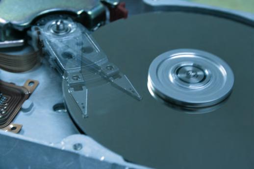
7 THIN FILM ANALYSIS Optimized Configuration 2 kev Ar + sputter depth profile of a multi-layer coating on a computer hard disk performed using Zalar rotation to enhance layer definition. A focused x-ray beam, high sensitivity spectrometer, high performance floating column argon ion gun, turnkey dual beam charge neutralization, compucentric Zalar rotation, and advanced data reduction algorithms provide the highest performance XPS depth profiling capability available. The standard monatomic argon ion gun is capable of generating 5 ev to 5 kev Ar ion beams and is ideally suited for most inorganic depth profiling applications. Inorganic Thin Film Analysis Floating column ion gun enables efficient low voltage depth profiling Bend in ion column to stop neutrals Compucentric Zalar rotation Robust dual beam charge neutralization Micro-area depth profiling Multi-point depth profiling


8 Ar 2500 CLUSTER SOURCE ION GUN OPTION Organic Depth Profiling It is well known that monatomic Ar ion guns used for inorganic thin film analysis typically cause severe chemical damage when sputtering most polymer and organic materials. PHI has led the way in developing and applying cluster source ion guns for the successful thin film analysis of polymer and organic materials. Our optional 20 kv Ar 2500 gas cluster ion gun and optional C 60 ion guns have proven performance for depth profiling many polymer and organic films while minimizing the potential for chemical damage. BPhen TCTA 10 kv Ar 2500 gas cluster ion beam sputter depth profile of a graded OLED test structure showing the ability to preserve and observe the two organic species that make up the test structure. The montage plot of N 1s spectra, on the right, shows the spectra that were used to create chemical state plots for N with the linear least squares fitting algorithm in PHI MultiPak.

9 C 60 CLUSTER SOURCE ION GUN OPTION Inorganic depth profiling With the introduction of cluster source ion guns for organic and polymer thin film depth profiling, interest has grown in applying these ion guns to inorganic structures that sustain chemical damage with monatomic Ar ion beam sputtering. Our experience has shown that some metalloids, oxides, and thin film structures that contain both organic and inorganic materials sustain less chemical damage and differential sputtering artifacts when depth profiled using a 20 kv C 60 cluster source ion gun. 20 kv C 60 sputter depth profile of an inverted organic photovoltaic device that contains metal layers, organic layers, oxide layers and a mixed matrix layer with an organic and TiO 2 nanorods. Compucentric Zalar rotation was used to enhance layer definition.

10 VERSATILE TEST CHAMBER CONFIGURATION Integrated Optional Accessories The VersaProbe III test chamber is designed to accept multiple photon and ion sources that are focused on a common analysis point on the sample and are all controlled from the SmartSoft user interface. Electron energy analyzer Optional UV light source for UPS Optional 20 kv Ar 2500 gas cluster ion gun Five axis automated sample manipulator Scanning x-ray source Optional UHV sample preparation chambers Sample introduction chamber Optional 20 kv C 60 gas cluster ion gun Monatomic Ar ion gun

11 CAPABILITIES Standard Features Scanned, micro-focused, monochromatic x-ray beam X-ray beam induced secondary electron imaging Dual beam charge neutralization 128 data channel detection Large area XPS Micro area XPS Chemical state imaging Multi-point sputter depth profiling Floating column monatomic Ar ion gun Compucentric Zalar rotation Angle dependent XPS Five axis automated sample manipulator 25 mm and 60 mm diameter sample holders Optional Accessories 10 kv C 60 ion gun 20 kv C 60 ion gun 20 kv Ar 2500 gas cluster ion gun 100 nm Scanning AES UV light source for UPS Dual anode, achromatic x-ray source Hot / Cold sample manipulator Custom sample preparation chambers
12 A DIVISION OF ULVAC-PHI Physical Electronics - USA Phone: sales@phi.com Web: ULVAC-PHI Inc. - Japan Phone: webmasterjp@phi.com Web:
A DIVISION OF ULVAC-PHI. Quantera II. Scanning XPS Microprobe
 A DIVISION OF ULVAC-PHI Quantera II Scanning XPS Microprobe X-ray Photoelectron Spectroscopy (XPS/ESCA) is the most widely used surface analysis technique and has many well established industrial and
PHI. Scanning XPS Microprobe
 PHI Scanning XPS Microprobe Unique Scanning XPS Microprobe X-ray photoelectron spectroscopy (XPS/ESA) is the most widely used surface analysis technique and has many well established industrial and research
PHI 5000 Versaprobe-II Focus X-ray Photo-electron Spectroscopy
 PHI 5000 Versaprobe-II Focus X-ray Photo-electron Spectroscopy The very basic theory of XPS XPS theroy Surface Analysis Ultra High Vacuum (UHV) XPS Theory XPS = X-ray Photo-electron Spectroscopy X-ray
Multi-technique photoelectron spectrometer for micro-area spectroscopy and imaging
 Multi-technique photoelectron spectrometer for micro-area spectroscopy and imaging U. Manju, M. Sreemony and A. K. Chakraborty In this note we present the new multipurpose photoelectron spectroscopy facility
Auger Electron Spectroscopy Overview
 Auger Electron Spectroscopy Overview Also known as: AES, Auger, SAM 1 Auger Electron Spectroscopy E KLL = E K - E L - E L AES Spectra of Cu EdN(E)/dE Auger Electron E N(E) x 5 E KLL Cu MNN Cu LMM E f E
A DIVISION OF ULVAC-PHI. Time-of-Flight Secondary Ion Mass Spectrometer with Parallel Imaging MS/MS for Confident Molecular Identification
 A DIVISION OF ULVAC-PHI Time-of-Flight Secondary Ion Mass Spectrometer with Parallel Imaging MS/MS for Confident Molecular Identification Designed for Confident Molecular Identification and Superior Imaging
PHI Model 06-C60 Sputter Ion Gun
 PHI Model 6-C6 Sputter Ion Gun Introduction: Physical Electronics introduced the model 6-C6 C 6 sputter ion gun and its unique capabilities for surface cleaning and depth profiling of soft materials (figure
Auger Electron Spectroscopy
 Auger Electron Spectroscopy Auger Electron Spectroscopy is an analytical technique that provides compositional information on the top few monolayers of material. Detect all elements above He Detection
X-Ray Photoelectron Spectroscopy (XPS) Prof. Paul K. Chu
 Prof. Paul K. Chu") X-Ray Photoelectron Spectroscopy (XPS) Prof. Paul K. Chu X-ray Photoelectron Spectroscopy Introduction Qualitative analysis Quantitative analysis Charging compensation Small area analysis and XPS imaging
X-Ray Photoelectron Spectroscopy (XPS) Prof. Paul K. Chu X-ray Photoelectron Spectroscopy Introduction Qualitative analysis Quantitative analysis Charging compensation Small area analysis and XPS imaging
Thermo Scientific K-Alpha + XPS Spectrometer. Fast, powerful and accessible chemical analysis for surface and thin film characterization
 Thermo Scientific K-Alpha + XPS Spectrometer Fast, powerful and accessible chemical analysis for surface and thin film characterization X-ray Photoelectron Spectroscopy Quantitative, chemical identification
Secondary Ion Mass Spectrometry (SIMS)
") CHEM53200: Lecture 10 Secondary Ion Mass Spectrometry (SIMS) Major reference: Surface Analysis Edited by J. C. Vickerman (1997). 1 Primary particles may be: Secondary particles can be e s, neutral species
CHEM53200: Lecture 10 Secondary Ion Mass Spectrometry (SIMS) Major reference: Surface Analysis Edited by J. C. Vickerman (1997). 1 Primary particles may be: Secondary particles can be e s, neutral species
Depth profiling of Organic Films using mixed C60 + and Ar + Ion-Sputtering
 Principle of Depth Profile Depth profiling of rganic Films using mixed C6 + and Ar + Ion-puttering putter Ion Beam Jing-Jong hyue, Ph.D. Analysis Depth ".5-1 nm# Research Center for Applied ciences, Academia
Hiden SIMS Secondary Ion Mass Spectrometers. Analysers for surface, elemental and molecular analysis
 Hiden SIMS Secondary Ion Mass Spectrometers Analysers for surface, elemental and molecular analysis vacuum analysis surface science plasma diagnostics gas analysis SIMS Versatility SIMS is a high sensitivity
The Benefit of Wide Energy Range Spectrum Acquisition During Sputter Depth Profile Measurements
 The Benefit of Wide Energy Range Spectrum Acquisition During Sputter Depth Profile Measurements Uwe Scheithauer, 82008 Unterhaching, Germany E-Mail: scht.uhg@googlemail.com Internet: orcid.org/0000-0002-4776-0678;
IONTOF. Latest Developments in 2D and 3D TOF-SIMS Analysis. Surface Analysis Innovations and Solutions for Industry 2017 Coventry
 Latest Developments in 2D and 3D TOF-SIMS Analysis Surface Analysis Innovations and Solutions for Industry 2017 Coventry 12.10.2017 Matthias Kleine-Boymann Regional Sales Manager matthias.kleine-boymann@iontof.com
Methods of surface analysis
 Methods of surface analysis Nanomaterials characterisation I RNDr. Věra Vodičková, PhD. Surface of solid matter: last monoatomic layer + absorbed monolayer physical properties are effected (crystal lattice
An Introduction to Auger Electron Spectroscopy
 An Introduction to Auger Electron Spectroscopy Spyros Diplas MENA3100 SINTEF Materials & Chemistry, Department of Materials Physics & Centre of Materials Science and Nanotechnology, Department of Chemistry,
Applications of XPS, AES, and TOF-SIMS
 Applications of XPS, AES, and TOF-SIMS Scott R. Bryan Physical Electronics 1 Materials Characterization Techniques Microscopy Optical Microscope SEM TEM STM SPM AFM Spectroscopy Energy Dispersive X-ray
CIG B5. Capitolato Tecnico Technical requirements
 Gara a procedura aperta per l'affidamento della fornitura di uno strumento per X-ray Photoelectron Spetroscopy (XPS) destinato alla Nanochemistry Facility dell Istituto Italiano di Tecnologia CIG 05092316B5
Technical description of photoelectron spectrometer Escalab 250Xi
 Technical description of photoelectron spectrometer Escalab 250Xi Resource center Physical Methods of Surface Investigations 2014 Table of contents Common description 3 Analytical chamber 8 Preparation
Dual Beam Helios Nanolab 600 and 650
 Dual Beam Helios Nanolab 600 and 650 In the Clean Room facilities of the INA LMA, several lithography facilities permit to pattern structures at the micro and nano meter scale and to create devices. In
MSE 321 Structural Characterization
 Auger Spectroscopy Auger Electron Spectroscopy (AES) Scanning Auger Microscopy (SAM) Incident Electron Ejected Electron Auger Electron Initial State Intermediate State Final State Physical Electronics
MSE 321 Structural Characterization
 Auger Spectroscopy Auger Electron Spectroscopy (AES) Scanning Auger Microscopy (SAM) Incident Electron Ejected Electron Auger Electron Initial State Intermediate State Final State Physical Electronics
ToF-SIMS or XPS? Xinqi Chen Keck-II
 ToF-SIMS or XPS? Xinqi Chen Keck-II 1 Time of Flight Secondary Ion Mass Spectrometry (ToF-SIMS) Not ToF MS (laser, solution) X-ray Photoelectron Spectroscopy (XPS) 2 3 Modes of SIMS 4 Secondary Ion Sputtering
Photoemission Spectroscopy
 FY13 Experimental Physics - Auger Electron Spectroscopy Photoemission Spectroscopy Supervisor: Per Morgen SDU, Institute of Physics Campusvej 55 DK - 5250 Odense S Ulrik Robenhagen,
Auger Electron Spectroscopy (AES)
") 1. Introduction Auger Electron Spectroscopy (AES) Silvia Natividad, Gabriel Gonzalez and Arena Holguin Auger Electron Spectroscopy (Auger spectroscopy or AES) was developed in the late 1960's, deriving
1. Introduction Auger Electron Spectroscopy (AES) Silvia Natividad, Gabriel Gonzalez and Arena Holguin Auger Electron Spectroscopy (Auger spectroscopy or AES) was developed in the late 1960's, deriving
Fig 1: Auger Electron Generation (a) Step 1 and (b) Step 2
 Step 1 and (b) Step 2") Auger Electron Spectroscopy (AES) Physics of AES: Auger Electrons were discovered in 1925 but were used in surface analysis technique in 1968. Auger Electron Spectroscopy (AES) is a very effective method
Auger Electron Spectroscopy (AES) Physics of AES: Auger Electrons were discovered in 1925 but were used in surface analysis technique in 1968. Auger Electron Spectroscopy (AES) is a very effective method
Large Area TOF-SIMS Imaging of the Antibacterial Distribution in Frozen-Hydrated Contact Lenses
 Large Area TOF-SIMS Imaging of the Antibacterial Distribution in Frozen-Hydrated Contact Lenses Overview: Imaging by time-of-flight secondary ion mass spectrometry (TOF-SIMS) is accomplished in a vacuum
for XPS surface analysis
 Thermo Scientific Avantage XPS Software Powerful instrument operation and data processing for XPS surface analysis Avantage Software Atomic Concentration (%) 100 The premier software for surface analysis
Application of Surface Analysis for Root Cause Failure Analysis
 Application of Surface Analysis for Root Cause Failure Analysis David A. Cole Evans Analytical Group East Windsor, NJ Specialists in Materials Characterization Outline Introduction X-Ray Photoelectron
Photoelectron spectroscopy Instrumentation. Nanomaterials characterization 2
 Photoelectron spectroscopy Instrumentation Nanomaterials characterization 2 RNDr. Věra V Vodičkov ková,, PhD. Photoelectron Spectroscopy general scheme Impact of X-ray emitted from source to the sample
AES - Auger Electron Spectrosopy
 Advanced Materials - Lab Intermediate Physics Ulm University Institute of Solid State Physics AES - Auger Electron Spectrosopy Sebastian Schnurr March 13, 2013 Safety Precautions MAKE SURE THAT YOU UNDERSTAND
Gaetano L Episcopo. Scanning Electron Microscopy Focus Ion Beam and. Pulsed Plasma Deposition
 Gaetano L Episcopo Scanning Electron Microscopy Focus Ion Beam and Pulsed Plasma Deposition Hystorical background Scientific discoveries 1897: J. Thomson discovers the electron. 1924: L. de Broglie propose
Auger Analyses Using Low Angle Incident Electrons
 Auger Analyses Using Low Angle Incident Electrons Kenichi Tsutsumi, Yuji agasawa and Toyohiko Tazawa Electron ptics Division, JEL Ltd. Introduction Auger Electron Spectroscopy (AES) is widely used, as
Characterization of Secondary Emission Materials for Micro-Channel Plates. S. Jokela, I. Veryovkin, A. Zinovev
 Characterization of Secondary Emission Materials for Micro-Channel Plates S. Jokela, I. Veryovkin, A. Zinovev Secondary Electron Yield Testing Technique We have incorporated XPS, UPS, Ar-ion sputtering,
The design of an integrated XPS/Raman spectroscopy instrument for co-incident analysis
 The design of an integrated XPS/Raman spectroscopy instrument for co-incident analysis Tim Nunney The world leader in serving science 2 XPS Surface Analysis XPS +... UV Photoelectron Spectroscopy UPS He(I)
XPS/UPS and EFM. Brent Gila. XPS/UPS Ryan Davies EFM Andy Gerger
 XPS/UPS and EFM Brent Gila XPS/UPS Ryan Davies EFM Andy Gerger XPS/ESCA X-ray photoelectron spectroscopy (XPS) also called Electron Spectroscopy for Chemical Analysis (ESCA) is a chemical surface analysis
Supplementary Information. Atomic Layer Deposition of Platinum Catalysts on Nanowire Surfaces for Photoelectrochemical Water Reduction
 Supplementary Information Atomic Layer Deposition of Platinum Catalysts on Nanowire Surfaces for Photoelectrochemical Water Reduction Neil P. Dasgupta 1 ǂ, Chong Liu 1,2 ǂ, Sean Andrews 1,2, Fritz B. Prinz
Introduction to X-ray Photoelectron Spectroscopy (XPS) XPS which makes use of the photoelectric effect, was developed in the mid-1960
 XPS which makes use of the photoelectric effect, was developed in the mid-1960") Introduction to X-ray Photoelectron Spectroscopy (XPS) X-ray Photoelectron Spectroscopy (XPS), also known as Electron Spectroscopy for Chemical Analysis (ESCA) is a widely used technique to investigate
Introduction to X-ray Photoelectron Spectroscopy (XPS) X-ray Photoelectron Spectroscopy (XPS), also known as Electron Spectroscopy for Chemical Analysis (ESCA) is a widely used technique to investigate
A Sustainable Synthesis of Nitrogen-Doped Carbon Aerogels
 A Sustainable Synthesis of Nitrogen-Doped Carbon Aerogels Supporting Information By Robin J. White, a, * Noriko Yoshizawa, b Markus Antonietti, a and Maria-Magdalena Titirici. a * e-mail: robin.white@mpikg.mpg.de
Advantages of coincident XPS-Raman in the analysis of mineral oxides species
 APPLICATION NOTE Advantages of coincident XPS-Raman in the analysis of mineral oxides species No. AN52950 Authors: Jon Treacy, Thermo Fisher Scientific, East Grinstead, Great Britain and Robert Heintz,
Auger Electron Spectroscopy (AES) Prof. Paul K. Chu
 Prof. Paul K. Chu") Auger Electron Spectroscopy (AES) Prof. Paul K. Chu Auger Electron Spectroscopy Introduction Principles Instrumentation Qualitative analysis Quantitative analysis Depth profiling Mapping Examples The Auger
Auger Electron Spectroscopy (AES) Prof. Paul K. Chu Auger Electron Spectroscopy Introduction Principles Instrumentation Qualitative analysis Quantitative analysis Depth profiling Mapping Examples The Auger
Electrochemical Deposition of Iron Nanoparticles on PPY and H terminated Si substrates. Karan Sukhija Co-op Term # 1 April 28 th, 2005
 Electrochemical Deposition of Iron Nanoparticles on PPY and H terminated Si substrates Karan Sukhija Co-op Term # 1 April 28 th, 2005 Future Suggested Experiments Acknowledgments Presentation Outline Background
Chemistry 311: Instrumentation Analysis Topic 2: Atomic Spectroscopy. Chemistry 311: Instrumentation Analysis Topic 2: Atomic Spectroscopy
 Topic 2b: X-ray Fluorescence Spectrometry Text: Chapter 12 Rouessac (1 week) 4.0 X-ray Fluorescence Download, read and understand EPA method 6010C ICP-OES Winter 2009 Page 1 Atomic X-ray Spectrometry Fundamental
VASE. J.A. Woollam Co., Inc. Ellipsometry Solutions
 VASE J.A. Woollam Co., Inc. Ellipsometry Solutions Accurate Capabilities The VASE is our most accurate and versatile ellipsometer for research on all types of materials: semiconductors, dielectrics, polymers,
Beamline practice at BL01B1 (XAFS) In-situ XAFS measurement of catalyst samples
 In-situ XAFS measurement of catalyst samples") Beamline practice at BL01B1 (XAFS) In-situ XAFS measurement of catalyst samples ver. 2015/09/18 T. Ina, K. Kato, T. Uruga (JASRI), P. Fons (AIST/JASRI) 1. Introduction The bending magnet beamline, BL01B1,
Beamline practice at BL01B1 (XAFS) In-situ XAFS measurement of catalyst samples ver. 2015/09/18 T. Ina, K. Kato, T. Uruga (JASRI), P. Fons (AIST/JASRI) 1. Introduction The bending magnet beamline, BL01B1,
Chapter 10. Nanometrology. Oxford University Press All rights reserved.
 Chapter 10 Nanometrology Oxford University Press 2013. All rights reserved. 1 Introduction Nanometrology is the science of measurement at the nanoscale level. Figure illustrates where nanoscale stands
X-Ray Photoelectron Spectroscopy XPS. Mark Engelhard
 X-Ray Photoelectron Spectroscopy XPS Mark Engelhard 1 Physical Electronics Quantera XPS High Energy Resolution Focused X-ray Beam Capability Glove box Glove box XPS glove box interface EMSL XPS Instrumentation
Surface and Interface Characterization of Polymer Films
 Surface and Interface Characterization of Polymer Films Jeff Shallenberger, Evans Analytical Group 104 Windsor Center Dr., East Windsor NJ Copyright 2013 Evans Analytical Group Outline Introduction to
Spin-resolved photoelectron spectroscopy
 Spin-resolved photoelectron spectroscopy Application Notes Spin-resolved photoelectron spectroscopy experiments were performed in an experimental station consisting of an analysis and a preparation chamber.
Chapter 12. Nanometrology. Oxford University Press All rights reserved.
 Chapter 12 Nanometrology Introduction Nanometrology is the science of measurement at the nanoscale level. Figure illustrates where nanoscale stands in relation to a meter and sub divisions of meter. Nanometrology
Modern Optical Spectroscopy
 Modern Optical Spectroscopy X-Ray Microanalysis Shu-Ping Lin, Ph.D. Institute of Biomedical Engineering E-mail: splin@dragon.nchu.edu.tw Website: http://web.nchu.edu.tw/pweb/users/splin/ Backscattered
Application of the GD-Profiler 2 to the PV domain
 Application of the GD-Profiler 2 to the PV domain GD Profiler 2 RF GDOES permits to follow the distribution of the elements as function of depth. This is an ultra fast characterisation technique capable
MICRO-TOMOGRAPHY AND X-RAY ANALYSIS OF GEOLOGICAL SAMPLES
 THE PUBLISHING HOUSE PROCEEDINGS OF THE ROMANIAN ACADEMY, Series A, OF THE ROMANIAN ACADEMY Volume 18, Number 1/2017, pp. 42 49 MICRO-TOMOGRAPHY AND X-RAY ANALYSIS OF GEOLOGICAL SAMPLES Ion GRUIA University
THIN FILMS FOR PHOTOVOLTAICS AND OTHER APPLICATIONS. BY Dr.A.K.SAXENA PHOTONICS DIVISION INDIAN INSTITUTE OF ASTROPHYSICS
 THIN FILMS FOR PHOTOVOLTAICS AND OTHER APPLICATIONS BY Dr.A.K.SAXENA PHOTONICS DIVISION INDIAN INSTITUTE OF ASTROPHYSICS BACKGROUND 2.8 meter coating plant at VBO, Kavalur 1.5 meter coating plant at VBO,
1 Introduction COPYRIGHTED MATERIAL. 1.1 HowdoweDefinetheSurface?
 1 Introduction JOHN C. VICKERMAN Manchester Interdisciplinary Biocentre, School of Chemical Engineering and Analytical Science, The University of Manchester, Manchester, UK The surface behaviour of materials
ABC s of Electrochemistry series Materials Characterization techniques: SEM and EDS Ana María Valenzuela-Muñiz November 3, 2011
 ABC s of Electrochemistry series Materials Characterization techniques: SEM and EDS Ana María Valenzuela-Muñiz November 3, 2011 CEER, Department of Chemical and Biomolecular Engineering Outline Introduction
Reduced preferential sputtering of TiO 2 (and Ta 2 O 5 ) thin films through argon cluster ion bombardment.
 thin films through argon cluster ion bombardment.") NATIOMEM Reduced preferential sputtering of TiO 2 (and Ta 2 O 5 ) thin films through argon cluster ion bombardment. R. Grilli *, P. Mack, M.A. Baker * * University of Surrey, UK ThermoFisher Scientific
NATIOMEM Reduced preferential sputtering of TiO 2 (and Ta 2 O 5 ) thin films through argon cluster ion bombardment. R. Grilli *, P. Mack, M.A. Baker * * University of Surrey, UK ThermoFisher Scientific
Lecture 5-8 Instrumentation
 Lecture 5-8 Instrumentation Requirements 1. Vacuum Mean Free Path Contamination Sticking probability UHV Materials Strength Stability Permeation Design considerations Pumping speed Virtual leaks Leaking
X-Ray Photoelectron Spectroscopy (XPS)
") X-Ray Photoelectron Spectroscopy (XPS) Louis Scudiero http://www.wsu.edu/~scudiero; 5-2669 Electron Spectroscopy for Chemical Analysis (ESCA) The basic principle of the photoelectric effect was enunciated
X-Ray Photoelectron Spectroscopy (XPS) Louis Scudiero http://www.wsu.edu/~scudiero; 5-2669 Electron Spectroscopy for Chemical Analysis (ESCA) The basic principle of the photoelectric effect was enunciated
IDRaman reader and IDRaman mini: Raster Orbital Scanning (ROS)
") IDRaman reader and IDRaman mini: Raster Orbital Scanning (ROS) Tightly focused beam may give noisy signals or miss the Raman active target completely leading to false negatives from unidentified samples
IDRaman reader and IDRaman mini: Raster Orbital Scanning (ROS) Tightly focused beam may give noisy signals or miss the Raman active target completely leading to false negatives from unidentified samples
structure and paramagnetic character R. Kakavandi, S-A. Savu, A. Caneschi, T. Chassé, M. B. Casu Electronic Supporting Information
 At the interface between organic radicals and TiO 2 (110) single crystals: electronic structure and paramagnetic character R. Kakavandi, S-A. Savu, A. Caneschi, T. Chassé, M. B. Casu Electronic Supporting
Defining quality standards for the analysis of solid samples
 Defining quality standards for the analysis of solid samples Thermo Scientific Element GD Plus Glow Discharge Mass Spectrometer Redefine your quality standards for the elemental analysis of solid samples
X Rays & Crystals. Characterizing Mineral Chemistry & Structure. J.D. Price
 X Rays & Crystals Characterizing Mineral Chemistry & Structure J.D. Price Light - electromagnetic spectrum Wave behavior vs. particle behavior If atoms are on the 10-10 m scale, we need to use sufficiently
TESCAN S New generation of FIB-SEM microscope
 TESCAN S New generation of FIB-SEM microscope rising standards in sample preparation Key Features SEM COLUMN Versatile system for unlimited applications: resolution imaging (0.9 nm at 15 kev, 1.4 nm at
Secondary Ion Mass Spectroscopy (SIMS)
") Secondary Ion Mass Spectroscopy (SIMS) Analyzing Inorganic Solids * = under special conditions ** = semiconductors only + = limited number of elements or groups Analyzing Organic Solids * = under special
Secondary Ion Mass Spectroscopy (SIMS) Analyzing Inorganic Solids * = under special conditions ** = semiconductors only + = limited number of elements or groups Analyzing Organic Solids * = under special
Catalysis CAPABILITIES
 Catalysis www.extrel.com CAPABILITIES Contents Extrel instruments have been recognized for their exceptional performance by the world s leading researchers for more than 50 years. Reliability and flexibility
Two-dimensional homologous perovskites as light absorbing materials for solar cell applications
 Supporting Information for Two-dimensional homologous perovskites as light absorbing materials for solar cell applications Duyen H. Cao, Constantinos C. Stoumpos, Omar K. Farha,, Joseph T. Hupp, and Mercouri
Keywords: Abstract. Uwe Scheithauer. Unterhaching
 Sputter Induced Cross Contaminations in Analytical AES and XPS Instrumentation: Utilization of the effect for the In situ Deposition of Ultrathin Functional Layers Uwe Scheithauer Unterhaching Phone: +49
Practical Surface Analysis
 Practical Surface Analysis SECOND EDITION Volume 1 Auger and X-ray Photoelectron Spectroscopy Edited by D. BRIGGS ICI PLC, Wilton Materials Research Centre, Wilton, Middlesbrough, Cleveland, UK and M.
X-ray Photoelectron Spectroscopy/ Electron spectroscopy for chemical analysis (ESCA), By Francis Chindeka
, By Francis Chindeka") X-ray Photoelectron Spectroscopy/ Electron spectroscopy for chemical analysis (ESCA), By Francis Chindeka X-ray photoelectron spectroscopy (XPS) or Electron spectroscopy for chemical analysis (ESCA), Surface
X-ray Photoelectron Spectroscopy/ Electron spectroscopy for chemical analysis (ESCA), By Francis Chindeka X-ray photoelectron spectroscopy (XPS) or Electron spectroscopy for chemical analysis (ESCA), Surface
X-Ray Photoelectron Spectroscopy (XPS)
") X-Ray Photoelectron Spectroscopy (XPS) Louis Scudiero http://www.wsu.edu/~scudiero; 5-2669 Fulmer 261A Electron Spectroscopy for Chemical Analysis (ESCA) The basic principle of the photoelectric effect
X-Ray Photoelectron Spectroscopy (XPS) Louis Scudiero http://www.wsu.edu/~scudiero; 5-2669 Fulmer 261A Electron Spectroscopy for Chemical Analysis (ESCA) The basic principle of the photoelectric effect
ABC s of Electrochemistry: X-Ray Photoelectron Spectroscopy (XPS) Madhivanan Muthuvel
 Madhivanan Muthuvel") ABC s of Electrochemistry: X-Ray Photoelectron Spectroscopy (XPS) Madhivanan Muthuvel Center for Electrochemical Engineering Research (CEER) Chemical and Biomolecular Engineering Ohio University Athens,
ABC s of Electrochemistry: X-Ray Photoelectron Spectroscopy (XPS) Madhivanan Muthuvel Center for Electrochemical Engineering Research (CEER) Chemical and Biomolecular Engineering Ohio University Athens,
QUESTIONS AND ANSWERS
 QUESTIONS AND ANSWERS (1) For a ground - state neutral atom with 13 protons, describe (a) Which element this is (b) The quantum numbers, n, and l of the inner two core electrons (c) The stationary state
TMT4320 Nanomaterials November 10 th, Thin films by physical/chemical methods (From chapter 24 and 25)
") 1 TMT4320 Nanomaterials November 10 th, 2015 Thin films by physical/chemical methods (From chapter 24 and 25) 2 Thin films by physical/chemical methods Vapor-phase growth (compared to liquid-phase growth)
1 TMT4320 Nanomaterials November 10 th, 2015 Thin films by physical/chemical methods (From chapter 24 and 25) 2 Thin films by physical/chemical methods Vapor-phase growth (compared to liquid-phase growth)
Characterization of plasma-treated surfaces by X-ray Photoelectron Spectroscopy (XPS)
") Characterization of plasma-treated surfaces by X-ray Photoelectron Spectroscopy (XPS) Teresa de los Arcos September 13, 2010 X-Ray photoelectron spectroscopy (XPS) is a technique used to determine the
Characterization of plasma-treated surfaces by X-ray Photoelectron Spectroscopy (XPS) Teresa de los Arcos September 13, 2010 X-Ray photoelectron spectroscopy (XPS) is a technique used to determine the
A COMPARATIVE CHEMICAL STUDY OF THE TOP LAYERS OF TWO DIFFERENT QUALITY SILICON SOLAR CELLS
 A COMPARATIVE CHEMICAL STUDY OF THE TOP LAYERS OF TWO DIFFERENT QUALITY SILICON SOLAR CELLS M.J. Ariza and D.Leinen Departamento de Fisica Aplicada I, Facultad de Ciencias, Universidad de Málaga, E-2971
raw materials C V Mn Mg S Al Ca Ti Cr Si G H Nb Na Zn Ni K Co A B C D E F
 Today s advanced batteries require a range of specialized analytical tools to better understand the electrochemical processes that occur during battery cycling. Evans Analytical Group (EAG) offers a wide-range
Secondary ion mass spectrometry (SIMS)
") Secondary ion mass spectrometry (SIMS) ELEC-L3211 Postgraduate Course in Micro and Nanosciences Department of Micro and Nanosciences Personal motivation and experience on SIMS Offers the possibility to
Secondary ion mass spectrometry (SIMS) ELEC-L3211 Postgraduate Course in Micro and Nanosciences Department of Micro and Nanosciences Personal motivation and experience on SIMS Offers the possibility to
Combinatorial RF Magnetron Sputtering for Rapid Materials Discovery: Methodology and Applications
 Combinatorial RF Magnetron Sputtering for Rapid Materials Discovery: Methodology and Applications Philip D. Rack,, Jason D. Fowlkes,, and Yuepeng Deng Department of Materials Science and Engineering University
Electron Microprobe Analysis 1 Nilanjan Chatterjee, Ph.D. Principal Research Scientist
 12.141 Electron Microprobe Analysis 1 Nilanjan Chatterjee, Ph.D. Principal Research Scientist Massachusetts Institute of Technology Electron Microprobe Facility Department of Earth, Atmospheric and Planetary
Lecture 22 Ion Beam Techniques
 Lecture 22 Ion Beam Techniques Schroder: Chapter 11.3 1/44 Announcements Homework 6/6: Will be online on later today. Due Wednesday June 6th at 10:00am. I will return it at the final exam (14 th June).
Auger Electron Spectrometry. EMSE-515 F. Ernst
 Auger Electron Spectrometry EMSE-515 F. Ernst 1 Principle of AES electron or photon in, electron out radiation-less transition Auger electron electron energy properties of atom 2 Brief History of Auger
Electron Microprobe Analysis 1 Nilanjan Chatterjee, Ph.D. Principal Research Scientist
 12.141 Electron Microprobe Analysis 1 Nilanjan Chatterjee, Ph.D. Principal Research Scientist Massachusetts Institute of Technology Electron Microprobe Facility Department of Earth, Atmospheric and Planetary
Nanoscale IR spectroscopy of organic contaminants
 The nanoscale spectroscopy company The world leader in nanoscale IR spectroscopy Nanoscale IR spectroscopy of organic contaminants Application note nanoir uniquely and unambiguously identifies organic
Imaging Methods: Scanning Force Microscopy (SFM / AFM)
") Imaging Methods: Scanning Force Microscopy (SFM / AFM) The atomic force microscope (AFM) probes the surface of a sample with a sharp tip, a couple of microns long and often less than 100 Å in diameter.
Imaging Methods: Scanning Force Microscopy (SFM / AFM) The atomic force microscope (AFM) probes the surface of a sample with a sharp tip, a couple of microns long and often less than 100 Å in diameter.
Introduction to SIMS Basic principles Components Techniques Drawbacks Figures of Merit Variations Resources
 Introduction to SIMS Basic principles Components Techniques Drawbacks Figures of Merit Variations Resources New technique for surface chemical analysis. SIMS examines the mass of ions, instead of energy
Dr. Tim Nunney Thermo Fisher Scientific, East Grinstead, UK Dr. Nick Bulloss Thermo Fisher Scientific, Madison, WI, USA Dr. Harry Meyer III Oak Ridge
 Dr. Tim Nunney Thermo Fisher Scientific, East Grinstead, UK Dr. Nick Bulloss Thermo Fisher Scientific, Madison, WI, USA Dr. Harry Meyer III Oak Ridge National Laboratory, TN, USA Introduction New materials
CHARACTERIZATION of NANOMATERIALS KHP
 CHARACTERIZATION of NANOMATERIALS Overview of the most common nanocharacterization techniques MAIN CHARACTERIZATION TECHNIQUES: 1.Transmission Electron Microscope (TEM) 2. Scanning Electron Microscope
Nova 600 NanoLab Dual beam Focused Ion Beam IITKanpur
 Nova 600 NanoLab Dual beam Focused Ion Beam system @ IITKanpur Dual Beam Nova 600 Nano Lab From FEI company (Dual Beam = SEM + FIB) SEM: The Electron Beam for SEM Field Emission Electron Gun Energy : 500
High Resolution Photoemission Study of the Spin-Dependent Band Structure of Permalloy and Ni
 High Resolution Photoemission Study of the Spin-Dependent Band Structure of Permalloy and Ni K. N. Altmann, D. Y. Petrovykh, and F. J. Himpsel Department of Physics, University of Wisconsin, Madison, 1150
X-ray photoelectron spectroscopy with a laser-plasma source
 Proc. SPIE Vol.3157 (1997) pp.176-183 X-ray photoelectron spectroscopy with a laser-plasma source Toshihisa TOMIE a, Hiroyuki KONDO b, Hideaki SHIMIZU a, and Peixiang Lu a a Electrotechnical Laboratory,
X-Ray Photoelectron Spectroscopy (XPS) Auger Electron Spectroscopy (AES)
 Auger Electron Spectroscopy (AES)") X-Ray Photoelectron Spectroscopy (XPS) Auger Electron Spectroscopy (AES) XPS X-ray photoelectron spectroscopy (XPS) is one of the most used techniques to chemically characterize the surface. Also known
X-Ray Photoelectron Spectroscopy (XPS) Auger Electron Spectroscopy (AES) XPS X-ray photoelectron spectroscopy (XPS) is one of the most used techniques to chemically characterize the surface. Also known
Electronic Supplementary Information: Synthesis and Characterization of Photoelectrochemical and Photovoltaic Cu2BaSnS4 Thin Films and Solar Cells
 Electronic Supplementary Material (ESI) for Journal of Materials Chemistry C. This journal is The Royal Society of Chemistry 2017 Electronic Supplementary Information: Synthesis and Characterization of
MS482 Materials Characterization ( 재료분석 ) Lecture Note 4: XRF
 Lecture Note 4: XRF") 2016 Fall Semester MS482 Materials Characterization ( 재료분석 ) Lecture Note 4: XRF Byungha Shin Dept. of MSE, KAIST 1 Course Information Syllabus 1. Overview of various characterization techniques (1 lecture)
2016 Fall Semester MS482 Materials Characterization ( 재료분석 ) Lecture Note 4: XRF Byungha Shin Dept. of MSE, KAIST 1 Course Information Syllabus 1. Overview of various characterization techniques (1 lecture)
UV-Vis optical fiber assisted spectroscopy in thin films and solutions
 UV-Vis optical fiber assisted spectroscopy in thin films and solutions Description UV-Visible absorption and transmission spectra provide fundamental information for all experiments related to the attenuation
Repeatability of Spectral Intensity Using an Auger Electron Spectroscopy Instrument Equipped with a Cylindrical Mirror Analyzer
 A. Kurokawa et al. Repeatability of Spectral Intensity Using an Auger lectron Spectroscopy Instrument quipped with a Cylindrical Mirror Analyzer Paper Repeatability of Spectral Intensity Using an Auger
Experimental 2.1 Introduction. Ultra high vacuum.
 2 Experimental 2.1 Introduction. Ultra high vacuum. The interest in solid-gas (or solid-vacuum) interfaces has been increasing rapidly during the last three decades. On one hand this is due to the practical
Segregated chemistry and structure on (001) and (100) surfaces of
 and (100) surfaces of") Supporting Information Segregated chemistry and structure on (001) and (100) surfaces of (La 1-x Sr x ) 2 CoO 4 override the crystal anisotropy in oxygen exchange kinetics Yan Chen a, Helena Téllez b,c,
Supporting Information Segregated chemistry and structure on (001) and (100) surfaces of (La 1-x Sr x ) 2 CoO 4 override the crystal anisotropy in oxygen exchange kinetics Yan Chen a, Helena Téllez b,c,
Energetic particles and their detection in situ (particle detectors) Part II. George Gloeckler
 Part II. George Gloeckler") Energetic particles and their detection in situ (particle detectors) Part II George Gloeckler University of Michigan, Ann Arbor, MI University of Maryland, College Park, MD Simple particle detectors Gas-filled
Energetic particles and their detection in situ (particle detectors) Part II George Gloeckler University of Michigan, Ann Arbor, MI University of Maryland, College Park, MD Simple particle detectors Gas-filled