Atmospheric pressure graphitization of SiC(0001) A route towards wafer-size graphene layers
|
|
|
- Esther Robbins
- 6 years ago
- Views:
Transcription
1 Atmospheric pressure graphitization of SiC(000) A route towards wafer-size graphene layers Konstantin V. Emtsev, Aaron Bostwick, Karsten Horn 3, Johannes Jobst 4, Gary L. Kellogg 5, Lothar Ley, Jessica L. McChesney, Taisuke Ohta 5, Sergey A. Reshanov 4, Eli Rotenberg, Andreas K. Schmid 6, Daniel Waldmann 4, Heiko B. Weber 4, Thomas Seyller,* Lehrstuhl für Technische Physik, Friedrich-Alexander-Universität Erlangen-Nürnberg, Erlangen, Germany Advanced Light Source, Lawrence Berkeley National Laboratory, Berkeley, CA, USA 3 Department of Molecular Physics, Fritz-Haber-Institut der Max-Planck-Gesellschaft, Berlin, Germany 4 Lehrstuhl für Angewandte Physik, Friedrich-Alexander-Universität Erlangen-Nürnberg, Erlangen, Germany 5 Sandia National Laboratories, Albuquerque, NM, USA 6 National Center for Electron Microscopy, Lawrence Berkeley National Laboratory, Berkeley, CA, USA * Corresponding author: thomas.seyller@physik.uni-erlangen.de Graphene, a single monolayer of graphite, has recently attracted considerable interest due to its novel magneto transport properties -3, high carrier mobility, and ballistic transport up to room temperature 4. It has technological applications as a potential successor of silicon for the post Moore s law era 5-7, as single molecule gas sensor 8, in spintronics 9-, in quantum computing, or as terahertz oscillators 3. For such applications, uniform ordered growth of graphene on an insulating substrate is necessary. While on the one hand exfoliation of graphene from graphite yields high quality crystals, such isolated samples with dimensions in the 0 micrometer range are unsuitable for large-scale device production; on the other hand the vacuum decomposition of SiC yields wafer-sized samples with small grains (30-00nm) that are equally unsuitable. Here we show that the ex-situ graphitization of Si-terminated SiC(000) in an argon atmosphere of about bar produces monolayer graphene films with much larger domain sizes than previously attainable. Hall measurements confirm the quality of the films thus obtained. For two different geometries, high electronic mobilities were found, which reach µ = 000 cm /Vs at T=7 K. A linear decrease of the mobility towards higher temperature is observed, which is presumably related to electron-electron
2 interaction. This method establishes the synthesis of graphene films on a technologically viable basis. The preparation of single layer graphene by the thermal decomposition of SiC is envisaged as a viable route for the synthesis of uniform, wafer-size graphene layers for technological applications, but the large scale structural quality is presently limited by the lack of continuity and uniformity of the grown film 5,6. On the Si-terminated (000) basal plane, vacuum annealing leads to small graphene domains typically nm in diameter, while on the C-terminated ( 000 ) face, larger domains (~00 nm) of multilayered, rotationally disordered graphene have been produced 4. The small-grain structure is due to morphological changes of the surface in the course of high temperature annealing. Moreover, decomposition of SiC is not a self-limiting process and, as a result, regions of different film thicknesses coexist, as shown by low-energy electron microscopy (LEEM) 5,6. Such inhomogeneous films do not meet the demands of large scale device production which requires larger grains and tighter thickness control. Homogeneous film thickness is particularly important because the electronic structure of the film depends strongly on the number of layers. For example, while monolayer graphene is a gapless semiconductor, a forbidden gap can be induced in bilayer graphene and tuned by an external electrostatic potential,7-0. We have devised a method of preparing graphene on SiC which results in a significantly improved film quality. Consider the data in Fig., where we compare samples prepared by vacuum annealing with samples produced by ex-situ annealing under argon atmosphere. Panels (a)-(c) show the morphology of the SiC (000) surface before and after the formation of a graphene monolayer by annealing in ultra high vacuum (UHV) as determined by atomic force microscopy (AFM) and LEEM. The initial SiC(000) surface in Fig.(a), obtained after hydrogen etching, is characterized by wide, highly uniform, atomically flat terraces. The step direction and terrace width (on the order of nm) are determined by the incidental misorientation of the substrate surface with respect to the crystallographic (000) plane. The step height is 5 Å which corresponds to the dimension of the 6H-SiC unit cell in the direction perpendicular to the surface (c-axis). On defect-free areas of the sample, the terraces typically extend undisturbed over 50 µm in length. The morphology of the surface covered with a monolayer of graphene prepared by vacuum annealing is shown in Fig. (b). The surface obviously undergoes significant modifications; it is now covered with small pits up to 0 nm in depth, and the original steps are hardly discernible any longer. This indicates that graphene growth is accompanied by substantial changes in the morphology of the substrate itself, leading to a considerable
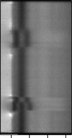
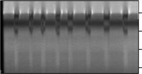
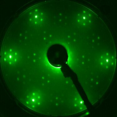
3 roughening. As a consequence of this roughening, the graphene layer acquires an inhomogeneous thickness distribution as can be seen in the LEEM image shown in Fig.(c). The irregularly-shaped graphene islands are at most a few hundred nm in size, in agreement with x- ray diffraction 4. Moreover, monolayer graphene areas coexist with graphene bilayer islands as well as with uncovered regions of the ( ) buffer layer. In stark contrast to the low quality resulting from vacuum graphitization (Fig. (b)), films grown under 900 mbar of argon have a greatly improved surface morphology, as demonstrated by the AFM image in Fig. (d). Step bunching is manifested by the formation of macro-terraces with a width that increases from about 0.5 µm on the original surface (Fig. (a)) to about 3 µm. Correspondingly, the macro-steps which are running in the same crystallographic direction as the original steps reach a height of about 5 nm. Parallel to the steps, uninterrupted macroterraces more than 50 µm long have been observed. The thickness distribution of the graphene film grown ex-situ under an argon atmosphere is determined by LEEM as shown in figs. (e,f). Series of spatially-resolved LEEM I-V spectra taken along a vertical and a horizontal line in fig. (f) are shown in figs. (g,h). The layer thickness is easily determined from the number of minima in the individual spectra; the LEEM image taken at a particular energy shows stripes that follow in width and orientation the macroterraces with a contrast that is determined by the graphene layer thickness. 5,6 Hence, we can unambiguously conclude that except for narrow stripes at the edges, the large atomically flat macro-terraces are homogeneously covered with a graphene monolayer. The domain size of monolayer graphene is significantly larger than that of the vacuum annealed samples as a comparison between figs. (c) and (f) shows. In fact, the domain size appears to be limited by the length and width of the SiC terraces only. Narrower, darker regions at the downward edges of the terraces correspond to bilayer and in some cases trilayer graphene (see region 3 in fig. (f)). In the AFM image these regions (see fig. (i)) appear as small depressions of around 4 Å and 8 Å amplitude located at the very edge of the macrostep. This indicates that the nucleation of new graphene layers starts at step edges of the substrate surface. We also note that the laterally averaged graphene thickness determined by LEEM is in perfect agreement with the average layer thickness value of. ML obtained by x-ray photoelectron spectroscopy (XPS). The graphene layers grown under an argon atmosphere exhibit high structural and electronic quality as demonstrated by the LEED and photoelectron spectroscopy data in Figure, taken from an Ar-grown film with a thickness of. ML. The LEED pattern demonstrates that
4 the graphene layer is well ordered and aligned with respect to the substrate, such that the basal plane unit vectors of graphene and SiC subtend an angle of 30 degrees. The Cs core level spectrum shows the characteristic signals of the SiC substrate, the ( ) interface layer and the graphene monolayer, respectively, in excellent agreement with previous work,. The angle-resolved photoelectron spectroscopy (ARPES) measurement reveals the characteristic band structure of monolayer graphene 0,3,4. Note that, as for vacuum grown layers 0,3,4, the Dirac point (E D ) is shifted below the Fermi level (E F ) due to electron doping from the substrate. Therefore, while our epitaxial growth process results in a dramatic improvement in surface morphology all other important properties such as crystalline order, electronic structure, and charge carrier density remain unaltered as compared to vacuum grown layers. What is the reason for the observed improvement of the surface morphology of the Arannealed samples compared to the samples annealed in UHV? From the data in Fig.. it is clear that the surface undergoes considerable morphological changes at the temperature where graphitization occurs. The large roughness of the UHV annealed samples suggests that the surface is far from equilibrium, such that a transformation to a smooth morphology cannot be achieved under these conditions. The key factor in achieving an improved growth is the significantly higher annealing temperature of 650 C that is required for graphene formation under argon at a pressure of 900 mbar as compared to 80 C in UHV. Graphene formation is the result of Si evaporation from the substrate. For a given temperature, the presence of a high pressure of argon leads to a reduced Si evaporation rate because the silicon atoms desorbing from the surface have a finite probability of being reflected back to the surface by collision with Ar atoms, as originally pointed out by Langmuir 5,6. The significantly higher growth temperature thus attained results in an enhancement of surface diffusion such that the restructuring of the surface that lowers the surface free energy (by step bunching, for example) is completed before graphene is formed. Ultimately, this leads to the dramatically improved surface morphology that we observe here. The macrostep structure is also responsible for the tighter thickness control. As shown above, a new graphene layer starts to grow from the step edges; hence having fewer steps along well defined crystallographic directions reduces the nucleation density of multilayer graphene. In order to evaluate the electronic quality of our graphene layers we determined the carrier mobility of monolayer epitaxial graphene on SiC(000) using Hall effect measurements. Two different geometries were investigated, both patterned with electron beam lithography: square graphene films (00 µm 00 µm) with contact pads at the four corners for van der Pauw
5 measurements as well as Hall bars ( µm 30 µm) placed on macroterraces. No significant difference in electron mobility was observed between the two geometries indicating that step edges play a minor role. Mobilities of 930 cm /Vs and 000 cm /Vs were measured at 300 and 7 K, respectively. At the same time the electron density remained basically constant n 0 3 cm increasing only by 3%. Experiments performed in other groups reported on maximum values of 00 cm /Vs, but on many-layer graphene 6,7. Figure 3 shows the temperature dependence of the electron mobility measured in van der Pauw geometry. The linear µ(t) dependence is unexpected. Scattering at acoustic phonons of graphene would result in T -4 behavior at low temperatures 8. A theoretical treatment of the effect of static impurities in graphene predicts /T dependence of the mobility 9. Candidates for such impurities are certainly dangling bonds below the graphene layer. Also adsorbates might play a certain role. The linear dependence of the scattering rates rather fits to the case of electronelectron interaction in a D electron gas 30. Clearly more work is required to understand the temperature dependence of the mobility in epitaxial graphene. In conclusion, we have shown that the growth of epitaxial graphene on SiC(000) in an Ar atmosphere close to atmospheric pressure provides morphologically superior graphene layers in comparison to vacuum graphitization. Extensive step bunching taking place during processing yields arrays of parallel terraces up to 3 µm wide and more than 50 µm long. The terraces are essentially completely and homogeneously covered with a monolayer of graphene. At present, downward step edges, where the initiation of second and third layer graphene growth is detected, are prohibiting an even larger extend of the graphene domains. Because the substrate step direction and step width are determined by the magnitude and azimuthal orientation of the surface misorientation with respect to major crystallographic directions, a proper choice of these parameters controls terrace width and length and hence the ultimate uninterrupted lateral extent of the graphene layer. An improved substrate quality in terms of crystallographic orientation is therefore expected to lead to further improvements. In comparison to the UHV treatment, the technique presented here is much closer to standard preparation conditions in semiconductor manufacture, permitting the use of standard CVD (chemical vapor deposition) equipment for the fabrication of graphene layers. All necessary processing steps, i.e. hydrogen etching and graphene synthesis, can be carried out in a single reactor. Electrical measurements confirm the picture of improved film quality: mobilities around 000 cm /Vs at room temperature, which increases linearly up to 000 cm /Vs at 7 K.
6 Methods Graphene layers were synthesized on commercial, nominally on-axis oriented wafers of 6H-SiC(000) purchased from SiCrystal AG. Prior to graphene epitaxy the samples were etched in hydrogen (grade 5.0, p= bar, T=550 C, t=5 minutes) in order to remove surface polishing damage. Graphene growth was carried out in a vertical cold wall reactor comprised of a doublewalled quartz tube and a graphite susceptor in a moderate flow of argon (5.0). Heating and cooling rates were -3 C per second. A wide range of annealing temperatures from 500 to 000 C and reactor gas pressures from 0 mbar to 900 mbar were tested and a detailed account of all observations will be provided elsewhere. Surface composition and graphene thicknesses were obtained from core-level photoelectron spectroscopy (XPS) by means of a Specs PHOIBOS50 analyzer in combination with a monochromatized Al K α source. Owing to the chemical inertness of graphene the samples can be easily transported through air. Asprepared graphene samples showed no detectable oxygen on the surface (below % of a monolayer) even after air exposure for about hour. Prolonged air exposure, however, leads to a fractional layer of physisorbed hydrocarbons and water which can be removed by annealing in vacuum at around 600 C. ARPES measurements were performed at the Advanced Light Source (ALS) using a Scienta R4000 analyzer. Core level measurements were performed at BESSY-II with a Specs PHOIBOS50 analyzer. The surface morphology was probed by atomic force microscopy (AFM) in non-contact mode. LEEM measurements were carried out at Sandia National Laboratory and at the National Center for Electron Microscopy, Lawrence Berkeley National Laboratory. The crystal structure of the films was monitored by low-energy electron diffraction (LEED). For the electrical characterization, the samples were patterened by two electron beam lithography steps: The first step defined the graphene film (undesired areas were etched with oxygen plasma). A second step defined the contact pads, which consist of thermally evaporated Ti/Au double layer, patterned by a standard lift-off technique. Electrical measurements in van der Pauw geometry or on Hall bar structures were carried out in a continuous flow cryostat (sample in vacuum), using magnetic fields of ±0.66 T at temperatures between 300 and 5 K. References Novoselov, K. S. et al., Two-dimensional gas of massless Dirac fermions in graphene. Nature 438, 97 (005). Zhang, Y. B., Tan, Y. W., Stormer, H. L., and Kim, P., Experimental observation of the quantum Hall effect and Berry's phase in graphene. Nature 438, 0 (005).
7 Novoselov, K. S. et al., Unconventional quantum Hall effect and Berry's phase of pi in bilayer graphene. Nat. Phys., 77 (006). Novoselov, K. S. et al., Room-Temperature Quantum Hall Effect in Graphene. Science, 370 (007). Geim, A. K. and Novoselov, K. S., The rise of graphene. Nat. Mater. 6, 83 (007). Berger, C. et al., Ultrathin epitaxial graphite: D electron gas properties and a route toward graphene-based nanoelectronics. J. Phys. Chem. B 08, 99 (004). Berger, C. et al., Electronic confinement and coherence in patterned epitaxial graphene. Science 3, 9 (006). Schedin, F. et al., Detection of individual gas molecules adsorbed on graphene. Nat. Mater. 6, 65 (007). Son, Y.-W., Cohen, M. L., and Louie, S. G., Half-metallic graphene nanoribbons. Nature 444, 347 (006). Trauzettel, B., Bulaev, D. V., Loss, D., and Burkard, G., Spin qubits in graphene quantum dots. Nat. Phys. 3 (3), 9 (007). Yokoyama, T., Controllable spin transport in ferromagnetic graphene junctions. Phys. Rev. B 77, (008). Fal'ko, V. I., Graphene: Quantum information on chicken wire. Nat. Phys. 3, 5 (007). Rana, F., Graphene Terahertz Plasmon Oscillators. IEEE Trans. Nanotechnol. 7, 9 (008). Hass, J. et al., Highly ordered graphene for two dimensional electronics. Appl. Phys. Lett. 89, 4306 (006). Hibino, H. et al., Microscopic thickness determination of thin graphite films formed on SiC from quantized oscillation in reflectivity of low-energy electrons. Phys. Rev. B 77, (008). Ohta, T. et al., Morphology of graphene thin film growth on SiC(000). New J. Phys. 0, (008). Guinea, F., Neto, A. H. Castro, and Peres, N. M. R., Electronic states and Landau levels in graphene stacks. Phys. Rev. B 73, 4546 (006). McCann, E., Asymmetry gap in the electronic band structure of bilayer graphene. Phys. Rev. B 74, 6403 (006). McCann, E. and Fal'ko, V. I., Landau-Level Degeneracy and Quantum Hall Effect in a Graphite Bilayer. Phys. Rev. Lett. 96, (006). Ohta, T. et al., Controlling the electronic structure of bilayer graphene. Science 33, 95 (006). Emtsev, K. V. et al., Interaction, growth, and ordering of epitaxial graphene on SiC{000} surfaces: A comparative photoelectron spectroscopy study. Phys. Rev. B 77, (008). Emtsev, K. V. et al., Initial stages of the graphite-sic(000) interface formation studied by photoelectron spectroscopy. Mater. Sci. Forum , 55 (007). Bostwick, A. et al., Quasiparticle dynamics in graphene. Nat. Phys. 3, 36 (007). Ohta, T. et al., Interlayer interaction and electronic screening in multilayer graphene. Phys. Rev. Lett. 98, 0680 (007). Langmuir, I., Convection and conduction of heat in gases. Phys. Rev. (Series I) 34, 40 (9). Fonda, G. R., Evaporation of tungsten under various pressures of argon. Phys. Rev. (Series II) 3, 60 (98). Kedzierski, J. et al., Epitaxial Graphene Transistors on SiC Substrates. IEEE Transactions on Electron Devices 55, 078 (008). Hwang, E. H. and Sarma, S. Das, Acoustic phonon scattering limited carrier mobility in two-dimensional extrinsic graphene. Phys. Rev. B 77, 5449 (008).
8 9 30 Cheianov, Vadim V. and Fal'ko, Vladimir I., Friedel Oscillations, Impurity Scattering, and Temperature Dependence of Resistivity in Graphene. Phys. Rev. Lett. 97, 680 (006). Zala, Gábor, Narozhny, B. N., and Aleiner, I. L., Interaction corrections at intermediate temperatures: Longitudinal conductivity and kinetic equation. Phys. Rev. B 64, 404 (00). Acknowledgements We gratefully acknowledge support by the DFG under contract SE 087/5-, contract WE454-5-, and within the Cluster of Excellence Engineering of Advanced Materials ( at the Friedrich-Alexander-Universität Erlangen-Nürnberg, and the BMBF under contract 05 ES3XBA/5. A part of the work was performed at Sandia National Laboratories, a multiprogram laboratory operated by Sandia Corporation, a Lockheed Martin company, for the United States Department of Energy, Office of Basic Energy Sciences, Division of Materials Science and Engineering, under Contract No. DE-AC04-94AL The work performed at the ALS supported by the Director, Office of Science, Office of Basic Energy Sciences, of the U.S. Department of Energy under Contract No. DE-AC03-76SF Correspondence and requests for materials should be addressed to T.S. (thomas.seyller@physik.uni-erlangen.de). Author Contributions K.E. performed the growth of graphene with the help of S.R. AFM measurements were done by K.E. and T.O. T.O. and A.S. carried out the LEEM measurements with the help of G.K. Photoelectron spectroscopy measurements were performed by K.E., T.S., A.B., J.M., E.R., and K.H. J. J., D. W., and H.B.W performed lithography and electrical measurements, T.S., K.E., and L.L. wrote the manuscript with revision and input from all other coauthors. Competing financial interests The authors declare that they have no competing financial interests.
9 Figure captions Fig : Morphological changes of 6H-SiC(000) during graphene growth. (a) Initial surface after H-etching imaged by AFM. The step height is 5 Å. (b) AFM image of graphene on 6H- SiC(000) with a nominal thickness of ML formed by annealing in UHV at a temperature of about 80 C. (c) LEEM image of a UHV grown graphene film on SiC(000) with a nominal thickness of. monolayers. The image contrast is due to the locally different layer thickness. Light, medium, and dark gray correspond to a local thickness of 0,, and ML, respectively. (d) AFM image of graphene on 6H-SiC(000) with a nominal thickness of. ML formed by annealing in Ar (p=900 mbar, T= 650 C). (e) LEEM image of a sample equivalent to that of (d) revealing macroterraces covered with graphene up to 50µm long and at least µm wide. (f) Close-up LEEM image revealing monolayer coverage on the terraces and bilayer/trilayer growth at the step edges. (g,h) Electron reflectivity spectra (gray scale images) taken at positions indicated by the blue lines in (f). Monolayer, bilayer, and trilayer graphene are readily identified by the presence of,, or 3 reflectivity minima, respectively. (i) Close-up AFM images of the film shown in (d). In the right hand side image the z-scale was adjusted such that the terraces appear at the same height. The profile shows that small depressions 4 and 8 Å in height exist at the step edges due to nd and 3 rd layer nucleation. Fig. Atomic and electronic structure of ex-situ grown monolayer graphene. (a) LEED pattern at 74 ev showing the diffraction spots due to the SiC(000) substrate (blue arrows) and the graphene lattice (red arrows). The additional spots are due to the ( ) interface layer. (b) Cs core level spectrum measured at a photon energy of 700 ev. The spectrum contains contributions from the SiC substrate (marked SiC), the ( ) interface layer (marked S and S), and from the graphene layer (G) residing on top of the interface layer. (c) π-bands probed by ARPES in the vicinity of the K-point of the hexagonal Brillouin zone. The position of the Dirac Energy (E D ) at 0.45 ev below the Fermi energy is consistent with previous reports on UHV grown graphene on SiC(000). Faint features marked in yellow signal the presence of small regions bilayer graphene in agreement with the LEEM results. Fig. 3. Temperature dependence of electron mobility in a monolayer epitaxial graphene. The mobility values were derived from Hall measurements on a sample in van der Pauw geometry. The experimental data display a linear T dependence. Qualitatively the same data have been measured for Hall effect geometries.


10 Fig. a d i A A B B 70nm 8.0µm b e.0µm 0µm c f g µm 0ML ML ML E=.9eV h 4µm 3 horiz. position energy (ev) 0 5 vert. position

11 Fig. a b c E D
12 Fig. 3
Atmospheric pressure graphitization of SiC(0001) A route towards wafer-size graphene layers
 A route towards wafer-size graphene layers") Atmospheric pressure graphitization of SiC(000) A route towards wafer-size graphene layers Konstantin V. Emtsev, Aaron Bostwick, Karsten Horn 3, Johannes Jobst 4, Gary L. Kellogg 5, Lothar Ley, Jessica
Atmospheric pressure graphitization of SiC(000) A route towards wafer-size graphene layers Konstantin V. Emtsev, Aaron Bostwick, Karsten Horn 3, Johannes Jobst 4, Gary L. Kellogg 5, Lothar Ley, Jessica
SUPPLEMENTARY INFORMATION
 SUPPLEMENTARY INFORMATION Towards wafer-size graphene layers by atmospheric pressure graphitization of silicon carbide Supporting online material Konstantin V. Emtsev 1, Aaron Bostwick 2, Karsten Horn
- 1 - Advanced Light Source, Lawrence Berkeley National Laboratory, Berkeley, California,
 - 1 - Morphology of graphene thin film growth on SiC(0001) Taisuke Ohta 1,2, Farid El Gabaly 3, Aaron Bostwick 1, Jessica McChesney 1,2, Konstantin V. Emtsev 4, Andreas K. Schmid 3, Thomas Seyller 4, Karsten
Optimizing Graphene Morphology on SiC(0001)
") Optimizing Graphene Morphology on SiC(0001) James B. Hannon Rudolf M. Tromp Graphene sheets Graphene sheets can be formed into 0D,1D, 2D, and 3D structures Chemically inert Intrinsically high carrier mobility
Optimizing Graphene Morphology on SiC(0001) James B. Hannon Rudolf M. Tromp Graphene sheets Graphene sheets can be formed into 0D,1D, 2D, and 3D structures Chemically inert Intrinsically high carrier mobility
Self-Doping Effects in Epitaxially-Grown Graphene. Abstract
 Self-Doping Effects in Epitaxially-Grown Graphene D.A.Siegel, 1,2 S.Y.Zhou, 1,2 F.ElGabaly, 3 A.V.Fedorov, 4 A.K.Schmid, 3 anda.lanzara 1,2 1 Department of Physics, University of California, Berkeley,
SiC Graphene Suitable For Quantum Hall Resistance Metrology.
 SiC Graphene Suitable For Quantum Hall Resistance Metrology. Samuel Lara-Avila 1, Alexei Kalaboukhov 1, Sara Paolillo, Mikael Syväjärvi 3, Rositza Yakimova 3, Vladimir Fal'ko 4, Alexander Tzalenchuk 5,
Graphene films on silicon carbide (SiC) wafers supplied by Nitride Crystals, Inc.
 wafers supplied by Nitride Crystals, Inc.") 9702 Gayton Road, Suite 320, Richmond, VA 23238, USA Phone: +1 (804) 709-6696 info@nitride-crystals.com www.nitride-crystals.com Graphene films on silicon carbide (SiC) wafers supplied by Nitride Crystals,
9702 Gayton Road, Suite 320, Richmond, VA 23238, USA Phone: +1 (804) 709-6696 info@nitride-crystals.com www.nitride-crystals.com Graphene films on silicon carbide (SiC) wafers supplied by Nitride Crystals,
Spin and angular resolved photoemission experiments on epitaxial graphene. Abstract
 Spin and angular resolved photoemission experiments on epitaxial graphene Isabella Gierz, 1, Jan Hugo Dil, 2, 3 Fabian Meier, 2, 3 Bartosz Slomski, 2, 3 Jürg Osterwalder, 3 Jürgen Henk, 4 Roland Winkler,
Low-temperature ballistic transport in nanoscale epitaxial graphene cross junctions
 Low-temperature ballistic transport in nanoscale epitaxial graphene cross junctions S. Weingart, C. Bock, and U. Kunze Werkstoffe und Nanoelektronik, Ruhr-Universität Bochum, D-44780 Bochum, Germany F.
Initial Stages of Growth of Organic Semiconductors on Graphene
 Initial Stages of Growth of Organic Semiconductors on Graphene Presented by: Manisha Chhikara Supervisor: Prof. Dr. Gvido Bratina University of Nova Gorica Outline Introduction to Graphene Fabrication
GRAPHENE ON THE Si-FACE OF SILICON CARBIDE USER MANUAL
 GRAPHENE ON THE Si-FACE OF SILICON CARBIDE USER MANUAL 1. INTRODUCTION Silicon Carbide (SiC) is a wide band gap semiconductor that exists in different polytypes. The substrate used for the fabrication
Graphene Novel Material for Nanoelectronics
 Graphene Novel Material for Nanoelectronics Shintaro Sato Naoki Harada Daiyu Kondo Mari Ohfuchi (Manuscript received May 12, 2009) Graphene is a flat monolayer of carbon atoms with a two-dimensional honeycomb
Overview. Carbon in all its forms. Background & Discovery Fabrication. Important properties. Summary & References. Overview of current research
 Graphene Prepared for Solid State Physics II Pr Dagotto Spring 2009 Laurene Tetard 03/23/09 Overview Carbon in all its forms Background & Discovery Fabrication Important properties Overview of current
TRANSVERSE SPIN TRANSPORT IN GRAPHENE
 International Journal of Modern Physics B Vol. 23, Nos. 12 & 13 (2009) 2641 2646 World Scientific Publishing Company TRANSVERSE SPIN TRANSPORT IN GRAPHENE TARIQ M. G. MOHIUDDIN, A. A. ZHUKOV, D. C. ELIAS,
Hydrogenated Graphene
 Hydrogenated Graphene Stefan Heun NEST, Istituto Nanoscienze-CNR and Scuola Normale Superiore Pisa, Italy Outline Epitaxial Graphene Hydrogen Chemisorbed on Graphene Hydrogen-Intercalated Graphene Outline
1. Theoretical predictions for charged impurity scattering in graphene
 Supplementary Information 1. Theoretical predictions for charged impurity scattering in graphene We briefly review the state of theoretical and experimental work on zeromagnetic-field charge transport
SUPPLEMENTARY INFORMATION
 DOI: 10.1038/NCHEM.2491 Experimental Realization of Two-dimensional Boron Sheets Baojie Feng 1, Jin Zhang 1, Qing Zhong 1, Wenbin Li 1, Shuai Li 1, Hui Li 1, Peng Cheng 1, Sheng Meng 1,2, Lan Chen 1 and
Supplementary Figure 1 Experimental setup for crystal growth. Schematic drawing of the experimental setup for C 8 -BTBT crystal growth.
 Supplementary Figure 1 Experimental setup for crystal growth. Schematic drawing of the experimental setup for C 8 -BTBT crystal growth. Supplementary Figure 2 AFM study of the C 8 -BTBT crystal growth
Intrinsic Electronic Transport Properties of High. Information
 Intrinsic Electronic Transport Properties of High Quality and MoS 2 : Supporting Information Britton W. H. Baugher, Hugh O. H. Churchill, Yafang Yang, and Pablo Jarillo-Herrero Department of Physics, Massachusetts
SUPPLEMENTARY INFORMATION
 SUPPLEMENTARY INFORMATION Facile Synthesis of High Quality Graphene Nanoribbons Liying Jiao, Xinran Wang, Georgi Diankov, Hailiang Wang & Hongjie Dai* Supplementary Information 1. Photograph of graphene
Graphene. Tianyu Ye November 30th, 2011
 Graphene Tianyu Ye November 30th, 2011 Outline What is graphene? How to make graphene? (Exfoliation, Epitaxial, CVD) Is it graphene? (Identification methods) Transport properties; Other properties; Applications;
Analysis of the Formation Conditions for Large Area Epitaxial Graphene on SiC Substrates
 Analysis of the Formation Conditions for Large Area Epitaxial Graphene on SiC Substrates Rositsa Yakimova, Chariya Virojanadara, Daniela Gogova, Mikael Syväjärvi, D. Siche, Krister Larsson and Leif Johansson
A. Optimizing the growth conditions of large-scale graphene films
 1 A. Optimizing the growth conditions of large-scale graphene films Figure S1. Optical microscope images of graphene films transferred on 300 nm SiO 2 /Si substrates. a, Images of the graphene films grown
LOW-TEMPERATURE Si (111) HOMOEPITAXY AND DOPING MEDIATED BY A MONOLAYER OF Pb
 HOMOEPITAXY AND DOPING MEDIATED BY A MONOLAYER OF Pb") LOW-TEMPERATURE Si (111) HOMOEPITAXY AND DOPING MEDIATED BY A MONOLAYER OF Pb O.D. DUBON, P.G. EVANS, J.F. CHERVINSKY, F. SPAEPEN, M.J. AZIZ, and J.A. GOLOVCHENKO Division of Engineering and Applied Sciences,
LOW-TEMPERATURE Si (111) HOMOEPITAXY AND DOPING MEDIATED BY A MONOLAYER OF Pb O.D. DUBON, P.G. EVANS, J.F. CHERVINSKY, F. SPAEPEN, M.J. AZIZ, and J.A. GOLOVCHENKO Division of Engineering and Applied Sciences,
Special Properties of Au Nanoparticles
 Special Properties of Au Nanoparticles Maryam Ebrahimi Chem 7500/750 March 28 th, 2007 1 Outline Introduction The importance of unexpected electronic, geometric, and chemical properties of nanoparticles
Observation of graphene on SiC using various types of microscopy
 SCIENTIFIC INSTRUMENT NEWS 06 Vol. 7 SEPTEMBER Technical magazine of Electron Microscope and Analytical Instruments. Article Observation of graphene on SiC using various types of microscopy Masao Nagase
An account of our efforts towards air quality monitoring in epitaxial graphene on SiC
 European Network on New Sensing Technologies for Air Pollution Control and Environmental Sustainability - EuNetAir COST Action TD1105 2 nd International Workshop EuNetAir on New Sensing Technologies for
Supplementary Figure S1. AFM images of GraNRs grown with standard growth process. Each of these pictures show GraNRs prepared independently,
 Supplementary Figure S1. AFM images of GraNRs grown with standard growth process. Each of these pictures show GraNRs prepared independently, suggesting that the results is reproducible. Supplementary Figure
Surface atoms/molecules of a material act as an interface to its surrounding environment;
 1 Chapter 1 Thesis Overview Surface atoms/molecules of a material act as an interface to its surrounding environment; their properties are often complicated by external adsorbates/species on the surface
Correlated 2D Electron Aspects of the Quantum Hall Effect
 Correlated 2D Electron Aspects of the Quantum Hall Effect Magnetic field spectrum of the correlated 2D electron system: Electron interactions lead to a range of manifestations 10? = 4? = 2 Resistance (arb.
Greg Andreev and Aravind Vijayaraghavan 9/27/13
 Mapping Graphene s surface potential with
Formation of Epitaxial Graphene on SiC(0001) using Vacuum or Argon Environments
 using Vacuum or Argon Environments") Formation of Epitaxial Graphene on SiC(0001) using Vacuum or Argon Environments Luxmi, N. Srivastava, and R. M. Feenstra Department of Physics, Carnegie Mellon University, Pittsburgh, PA 15213 P. J. Fisher
Formation of Epitaxial Graphene on SiC(0001) using Vacuum or Argon Environments Luxmi, N. Srivastava, and R. M. Feenstra Department of Physics, Carnegie Mellon University, Pittsburgh, PA 15213 P. J. Fisher
Graphene: Plane and Simple Electrical Metrology?
 Graphene: Plane and Simple Electrical Metrology? R. E. Elmquist, F. L. Hernandez-Marquez, M. Real, T. Shen, D. B. Newell, C. J. Jacob, and G. R. Jones, Jr. National Institute of Standards and Technology,
SUPPLEMENTARY INFORMATION
 DOI: 1.138/NMAT3449 Topological crystalline insulator states in Pb 1 x Sn x Se Content S1 Crystal growth, structural and chemical characterization. S2 Angle-resolved photoemission measurements at various
Single-Molecule Junctions: Vibrational and Magnetic Degrees of Freedom, and Novel Experimental Techniques
 Single-Molecule Junctions: Vibrational and Magnetic Degrees of Freedom, and Novel Experimental Techniques Heiko B. Weber Lehrstuhl für Angewandte Physik Friedrich-Alexander-Universität Erlangen-Nürnberg
SUPPLEMENTARY INFORMATION
 Dirac electron states formed at the heterointerface between a topological insulator and a conventional semiconductor 1. Surface morphology of InP substrate and the device Figure S1(a) shows a 10-μm-square
Supplementary Figure 1 Magneto-transmission spectra of graphene/h-bn sample 2 and Landau level transition energies of three other samples.
 Supplementary Figure 1 Magneto-transmission spectra of graphene/h-bn sample 2 and Landau level transition energies of three other samples. (a,b) Magneto-transmission ratio spectra T(B)/T(B 0 ) of graphene/h-bn
Growth of Embedded and Protrusive Striped Graphene on 6H-SiC (0001)
") Growth of Embedded and Protrusive Striped Graphene on 6H-SiC (0001) A. Ruammaitree, H. Nakahara, K. Soda, Y. Saito Department of Quantum Engineering, Faculty of Engineering, Nagoya University, Nagoya 464-8603
Growth of Embedded and Protrusive Striped Graphene on 6H-SiC (0001) A. Ruammaitree, H. Nakahara, K. Soda, Y. Saito Department of Quantum Engineering, Faculty of Engineering, Nagoya University, Nagoya 464-8603
Epitaxial graphene on SiC formed by the surface structure control technique
 Epitaxial graphene on SiC formed by the surface structure control technique Takuya Aritsuki*, Takeshi Nakashima, Keisuke Kobayashi, Yasuhide Ohno, and Masao Nagase Tokushima University, Tokushima 770-8506,
Electronic states on the surface of graphite
 Electronic states on the surface of graphite Guohong Li, Adina Luican, Eva Y. Andrei * Department of Physics and Astronomy, Rutgers Univsersity, Piscataway, NJ 08854, USA Elsevier use only: Received date
SUPPLEMENTARY FIGURES
 1 SUPPLEMENTARY FIGURES Supplementary Figure 1: Initial stage showing monolayer MoS 2 islands formation on Au (111) surface. a, Scanning tunneling microscopy (STM) image of molybdenum (Mo) clusters deposited
Solid Surfaces, Interfaces and Thin Films
 Hans Lüth Solid Surfaces, Interfaces and Thin Films Fifth Edition With 427 Figures.2e Springer Contents 1 Surface and Interface Physics: Its Definition and Importance... 1 Panel I: Ultrahigh Vacuum (UHV)
SUPPLEMENTARY INFORMATION
 DOI: 1.138/NNANO.211.214 Control over topological insulator photocurrents with light polarization J.W. McIver*, D. Hsieh*, H. Steinberg, P. Jarillo-Herrero and N. Gedik SI I. Materials and device fabrication
Impact of Calcium on Transport Property of Graphene. Jyoti Katoch and Masa Ishigami*
 Impact of Calcium on Transport Property of Graphene Jyoti Katoch and Masa Ishigami* Department of Physics and Nanoscience Technology Center, University of Central Florida, Orlando, FL, 32816 *Corresponding
Guowei He, N. Srivastava, R. M. Feenstra * Dept. Physics, Carnegie Mellon University, Pittsburgh, PA 15213
 Formation of Graphene on SiC( 0001 ) Surfaces in Disilane and Neon Environments Guowei He, N. Srivastava, R. M. Feenstra * Dept. Physics, Carnegie Mellon University, Pittsburgh, PA 15213 Abstract The formation
Graphene Fundamentals and Emergent Applications
 Graphene Fundamentals and Emergent Applications Jamie H. Warner Department of Materials University of Oxford Oxford, UK Franziska Schaffel Department of Materials University of Oxford Oxford, UK Alicja
Raman spectroscopy study of rotated double-layer graphene: misorientation angle dependence of electronic structure
 Supplementary Material for Raman spectroscopy study of rotated double-layer graphene: misorientation angle dependence of electronic structure Kwanpyo Kim 1,2,3, Sinisa Coh 1,3, Liang Z. Tan 1,3, William
Carbon based Nanoscale Electronics
 Carbon based Nanoscale Electronics 09 02 200802 2008 ME class Outline driving force for the carbon nanomaterial electronic properties of fullerene exploration of electronic carbon nanotube gold rush of
Structure analysis: Electron diffraction LEED TEM RHEED
 Structure analysis: Electron diffraction LEED: Low Energy Electron Diffraction SPA-LEED: Spot Profile Analysis Low Energy Electron diffraction RHEED: Reflection High Energy Electron Diffraction TEM: Transmission
CVD growth of Graphene. SPE ACCE presentation Carter Kittrell James M. Tour group September 9 to 11, 2014
 CVD growth of Graphene SPE ACCE presentation Carter Kittrell James M. Tour group September 9 to 11, 2014 Graphene zigzag armchair History 1500: Pencil-Is it made of lead? 1789: Graphite 1987: The first
Yugang Sun Center for Nanoscale Materials, Argonne National Laboratory, Argonne, IL 60439
 Morphology of Graphene on SiC( 000 1 ) Surfaces Luxmi, P. J. Fisher, N. Srivastava, and R. M. Feenstra Dept. Physics, Carnegie Mellon University, Pittsburgh, PA 15213 Yugang Sun Center for Nanoscale Materials,
Epitaxial graphene on SiC(0001): More than just honeycombs. Y. Qi, S. H. Rhim, G. F. Sun, M. Weinert, and L. Li*
: More than just honeycombs. Y. Qi, S. H. Rhim, G. F. Sun, M. Weinert, and L. Li*") Epitaxial graphene on SiC(0001): More than just honeycombs Y. Qi, S. H. Rhim, G. F. Sun, M. Weinert, and L. Li* Department of Physics and Laboratory for Surface Studies University of Wisconsin, Milwaukee,
Epitaxial graphene on SiC(0001): More than just honeycombs Y. Qi, S. H. Rhim, G. F. Sun, M. Weinert, and L. Li* Department of Physics and Laboratory for Surface Studies University of Wisconsin, Milwaukee,
Impact of disorder and topology in two dimensional systems at low carrier densities
 Impact of disorder and topology in two dimensional systems at low carrier densities A Thesis Submitted For the Degree of Doctor of Philosophy in the Faculty of Science by Mohammed Ali Aamir Department
structure and paramagnetic character R. Kakavandi, S-A. Savu, A. Caneschi, T. Chassé, M. B. Casu Electronic Supporting Information
 At the interface between organic radicals and TiO 2 (110) single crystals: electronic structure and paramagnetic character R. Kakavandi, S-A. Savu, A. Caneschi, T. Chassé, M. B. Casu Electronic Supporting
Graphene Formation on the Carbon face of Silicon Carbide
 Carnegie Mellon University Research Showcase @ CMU Dissertations Theses and Dissertations Summer 9-2014 Graphene Formation on the Carbon face of Silicon Carbide Guowei He Carnegie Mellon University Follow
Quantum transport through graphene nanostructures
 Quantum transport through graphene nanostructures S. Rotter, F. Libisch, L. Wirtz, C. Stampfer, F. Aigner, I. Březinová, and J. Burgdörfer Institute for Theoretical Physics/E136 December 9, 2009 Graphene
XPS Depth Profiling of Epitaxial Graphene Intercalated with FeCl 3
 XPS Depth Profiling of Epitaxial Graphene Intercalated with FeCl 3 Mahdi Ibrahim Maynard H. Jackson High School Atlanta, GA. Faculty Advisor: Dr. Kristin Shepperd Research Group: Prof. Edward Conrad School
Decoupling Graphene from SiC(0001) via Oxidation
 via Oxidation") Decoupling Graphene from SiC(0001) via Oxidation S. Oida, F.R. McFeely, J.B. Hannon, R.M. Tromp, M. Copel, Z. Chen, Y. Sun, D.B. Farmer and J. Yurkas 1 IBM Research Division, T.J. Watson Research Center,
Decoupling Graphene from SiC(0001) via Oxidation S. Oida, F.R. McFeely, J.B. Hannon, R.M. Tromp, M. Copel, Z. Chen, Y. Sun, D.B. Farmer and J. Yurkas 1 IBM Research Division, T.J. Watson Research Center,
Spin-resolved photoelectron spectroscopy
 Spin-resolved photoelectron spectroscopy Application Notes Spin-resolved photoelectron spectroscopy experiments were performed in an experimental station consisting of an analysis and a preparation chamber.
Energy Spectroscopy. Ex.: Fe/MgO
 Energy Spectroscopy Spectroscopy gives access to the electronic properties (and thus chemistry, magnetism,..) of the investigated system with thickness dependence Ex.: Fe/MgO Fe O Mg Control of the oxidation
Supporting Information. by Hexagonal Boron Nitride
 Supporting Information High Velocity Saturation in Graphene Encapsulated by Hexagonal Boron Nitride Megan A. Yamoah 1,2,, Wenmin Yang 1,3, Eric Pop 4,5,6, David Goldhaber-Gordon 1 * 1 Department of Physics,
Supplementary Figure S1. AFM characterizations and topographical defects of h- BN films on silica substrates. (a) (c) show the AFM height
 (c) show the AFM height") Supplementary Figure S1. AFM characterizations and topographical defects of h- BN films on silica substrates. (a) (c) show the AFM height topographies of h-bn film in a size of ~1.5µm 1.5µm, 30µm 30µm
Supplementary Figure S1. AFM characterizations and topographical defects of h- BN films on silica substrates. (a) (c) show the AFM height topographies of h-bn film in a size of ~1.5µm 1.5µm, 30µm 30µm
Graphene and Carbon Nanotubes
 Graphene and Carbon Nanotubes 1 atom thick films of graphite atomic chicken wire Novoselov et al - Science 306, 666 (004) 100μm Geim s group at Manchester Novoselov et al - Nature 438, 197 (005) Kim-Stormer
Frictional characteristics of exfoliated and epitaxial graphene
 Frictional characteristics of exfoliated and epitaxial graphene Young Jun Shin a,b, Ryan Stromberg c, Rick Nay c, Han Huang d, Andrew T. S. Wee d, Hyunsoo Yang a,b,*, Charanjit S. Bhatia a a Department
Graphene devices and integration: A primer on challenges
 Graphene devices and integration: A primer on challenges Archana Venugopal (TI) 8 Nov 2016 Acknowledgments: Luigi Colombo (TI) UT Dallas and UT Austin 1 Outline Where we are Issues o Contact resistance
Growing Graphene on Semiconductors
 Growing Graphene on Semiconductors edited by Nunzio Motta Francesca Iacopi Camilla Coletti Growing Graphene on Semiconductors Growing Graphene on Semiconductors edited by Nunzio Motta Francesca Iacopi
Magneto-plasmonic effects in epitaxial graphene
 Magneto-plasmonic effects in epitaxial graphene Alexey Kuzmenko University of Geneva Graphene Nanophotonics Benasque, 4 March 13 Collaborators I. Crassee, N. Ubrig, I. Nedoliuk, J. Levallois, D. van der
Transversal electric field effect in multilayer graphene nanoribbon
 Transversal electric field effect in multilayer graphene nanoribbon S. Bala kumar and Jing Guo a) Department of Electrical and Computer Engineering, University of Florida, Gainesville, Florida 32608, USA
Single-Molecule Junctions with Epitaxial. Graphene Nanoelectrodes. (Supporting Information)
") Single-Molecule Junctions with Epitaxial Graphene Nanoelectrodes (Supporting Information) Konrad Ullmann, Pedro B. Coto, Susanne Leitherer, Agustín Molina-Ontoria,, Nazario Martín, Michael Thoss, and Heiko
Single-Molecule Junctions with Epitaxial Graphene Nanoelectrodes (Supporting Information) Konrad Ullmann, Pedro B. Coto, Susanne Leitherer, Agustín Molina-Ontoria,, Nazario Martín, Michael Thoss, and Heiko
8 Summary and outlook
 91 8 Summary and outlook The main task of present work was to investigate the growth, the atomic and the electronic structures of Co oxide as well as Mn oxide films on Ag(001) by means of STM/STS at LT
1. Nanotechnology & nanomaterials -- Functional nanomaterials enabled by nanotechnologies.
 Novel Nano-Engineered Semiconductors for Possible Photon Sources and Detectors NAI-CHANG YEH Department of Physics, California Institute of Technology 1. Nanotechnology & nanomaterials -- Functional nanomaterials
.Fritjaf Capra, The Tao of Physics
 Probing inside the atom and investigating its structure, science transcended the limits of our sensory imagination. From this point on, it could no longer rely with absolute certainty on logic and common
performance electrocatalytic or electrochemical devices. Nanocrystals grown on graphene could have
 Nanocrystal Growth on Graphene with Various Degrees of Oxidation Hailiang Wang, Joshua Tucker Robinson, Georgi Diankov, and Hongjie Dai * Department of Chemistry and Laboratory for Advanced Materials,
Wafer-scale fabrication of graphene
 Wafer-scale fabrication of graphene Sten Vollebregt, MSc Delft University of Technology, Delft Institute of Mircosystems and Nanotechnology Delft University of Technology Challenge the future Delft University
Raman Imaging and Electronic Properties of Graphene
 Raman Imaging and Electronic Properties of Graphene F. Molitor, D. Graf, C. Stampfer, T. Ihn, and K. Ensslin Laboratory for Solid State Physics, ETH Zurich, 8093 Zurich, Switzerland ensslin@phys.ethz.ch
Supplementary Figure 1: MoS2 crystals on WSe2-EG and EG and WSe2 crystals on MoSe2-EG and EG.
 Supplementary Figure 1: MoS2 crystals on WSe2-EG and EG and WSe2 crystals on MoSe2-EG and EG. (a) The MoS2 crystals cover both of EG and WSe2/EG after the CVD growth (Scar bar: 400 nm) (b) shows TEM profiles
Exceptional ballistic transport in epigraphene. Walt de Heer Georgia Institute of Technology
 Exceptional ballistic transport in epigraphene Walt de Heer Georgia Institute of Technology Program Objective First formulated in 2001 and patented in 2003, our objective is to develop nanoelectronics
Introduction to Nanotechnology Chapter 5 Carbon Nanostructures Lecture 1
 Introduction to Nanotechnology Chapter 5 Carbon Nanostructures Lecture 1 ChiiDong Chen Institute of Physics, Academia Sinica chiidong@phys.sinica.edu.tw 02 27896766 Carbon contains 6 electrons: (1s) 2,
Emergence of a Metal-Insulator Transition and High Temperature Charge Density Waves in VSe 2 at the Monolayer Limit
 Supporting Information Emergence of a Metal-Insulator Transition and High Temperature Charge Density Waves in VSe 2 at the Monolayer Limit Ganbat Duvjir, Byoung Ki Choi, Iksu Jang, Søren Ulstrup,, Soonmin
Broken Symmetry States and Divergent Resistance in Suspended Bilayer Graphene
 Broken Symmetry States and Divergent Resistance in Suspended Bilayer Graphene The Harvard community has made this article openly available. Please share how this access benefits you. Your story matters.
Graphene FETs EE439 FINAL PROJECT. Yiwen Meng Su Ai
 Graphene FETs EE439 FINAL PROJECT Yiwen Meng Su Ai Introduction What is Graphene? An atomic-scale honeycomb lattice made of carbon atoms Before 2004, Hypothetical Carbon Structure Until 2004, physicists
Coupled perpendicular magnetization in Fe/Cu/Fe trilayers
 Journal of Magnetism and Magnetic Materials 300 (2006) 479 483 www.elsevier.com/locate/jmmm Coupled perpendicular magnetization in Fe/Cu/Fe trilayers D. Repetto, A. Enders, K. Kern Max Planck Institut
Lithography-free Fabrication of High Quality Substrate-supported and. Freestanding Graphene devices
 Lithography-free Fabrication of High Quality Substrate-supported and Freestanding Graphene devices W. Bao 1, G. Liu 1, Z. Zhao 1, H. Zhang 1, D. Yan 2, A. Deshpande 3, B.J. LeRoy 3 and C.N. Lau 1, * 1
High Resolution Photoemission Study of the Spin-Dependent Band Structure of Permalloy and Ni
 High Resolution Photoemission Study of the Spin-Dependent Band Structure of Permalloy and Ni K. N. Altmann, D. Y. Petrovykh, and F. J. Himpsel Department of Physics, University of Wisconsin, Madison, 1150
Supporting Information
 Supporting Information Yao et al. 10.1073/pnas.1416368111 Fig. S1. In situ LEEM imaging of graphene growth via chemical vapor deposition (CVD) on Pt(111). The growth of graphene on Pt(111) via a CVD process
Transport Properties of Graphene Nanoribbon Transistors on. Chemical-Vapor-Deposition Grown Wafer-Scale Graphene
 Transport Properties of Graphene Nanoribbon Transistors on Chemical-Vapor-Deposition Grown Wafer-Scale Graphene Wan Sik Hwang 1, a), Kristof Tahy 1, Xuesong Li 2, Huili (Grace) Xing 1, Alan C. Seabaugh
Nanostructure. Materials Growth Characterization Fabrication. More see Waser, chapter 2
 Nanostructure Materials Growth Characterization Fabrication More see Waser, chapter 2 Materials growth - deposition deposition gas solid Physical Vapor Deposition Chemical Vapor Deposition Physical Vapor
Graphene and Quantum Hall (2+1)D Physics
D Physics") The 4 th QMMRC-IPCMS Winter School 8 Feb 2011, ECC, Seoul, Korea Outline 2 Graphene and Quantum Hall (2+1)D Physics Lecture 1. Electronic structures of graphene and bilayer graphene Lecture 2. Electrons
The 4 th QMMRC-IPCMS Winter School 8 Feb 2011, ECC, Seoul, Korea Outline 2 Graphene and Quantum Hall (2+1)D Physics Lecture 1. Electronic structures of graphene and bilayer graphene Lecture 2. Electrons
SUPPLEMENTARY INFORMATION
 SUPPLEMENTARY INFORMATION SUPPLEMENTARY INFORMATION Trilayer graphene is a semimetal with a gate-tuneable band overlap M. F. Craciun, S. Russo, M. Yamamoto, J. B. Oostinga, A. F. Morpurgo and S. Tarucha
3-month progress Report
 3-month progress Report Graphene Devices and Circuits Supervisor Dr. P.A Childs Table of Content Abstract... 1 1. Introduction... 1 1.1 Graphene gold rush... 1 1.2 Properties of graphene... 3 1.3 Semiconductor
File name: Supplementary Information Description: Supplementary Figures, Supplementary Notes, Supplementary Tables, Supplementary References
 File name: Supplementary Information Description: Supplementary Figures, Supplementary Notes, Supplementary Tables, Supplementary References Supplementary Figure 1 Illustration of the reaction chamber
2D MBE Activities in Sheffield. I. Farrer, J. Heffernan Electronic and Electrical Engineering The University of Sheffield
 2D MBE Activities in Sheffield I. Farrer, J. Heffernan Electronic and Electrical Engineering The University of Sheffield Outline Motivation Van der Waals crystals The Transition Metal Di-Chalcogenides
& Dirac Fermion confinement Zahra Khatibi
 Graphene & Dirac Fermion confinement Zahra Khatibi 1 Outline: What is so special about Graphene? applications What is Graphene? Structure Transport properties Dirac fermions confinement Necessity External
ConceptGraphene. Small or medium-scale focused research project. WP4 Spin transport devices
 ConceptGraphene New Electronics Concept: Wafer-Scale Epitaxial Graphene Small or medium-scale focused research project WP4 Spin transport devices Deliverable 4.1 Report on spin transport in graphene on
Supporting Information Available:
 Supporting Information Available: Photoresponsive and Gas Sensing Field-Effect Transistors based on Multilayer WS 2 Nanoflakes Nengjie Huo 1, Shengxue Yang 1, Zhongming Wei 2, Shu-Shen Li 1, Jian-Bai Xia
Quantum Hall effect and Landau level crossing of Dirac fermions in trilayer graphene Supplementary Information
 Quantum Hall effect and Landau level crossing of Dirac fermions in trilayer graphene Supplementary Information Thiti Taychatanapat, Kenji Watanabe, Takashi Taniguchi, Pablo Jarillo-Herrero Department of
Ferromagnetism and Anomalous Hall Effect in Graphene
 Ferromagnetism and Anomalous Hall Effect in Graphene Jing Shi Department of Physics & Astronomy, University of California, Riverside Graphene/YIG Introduction Outline Proximity induced ferromagnetism Quantized
Black phosphorus: A new bandgap tuning knob
 Black phosphorus: A new bandgap tuning knob Rafael Roldán and Andres Castellanos-Gomez Modern electronics rely on devices whose functionality can be adjusted by the end-user with an external knob. A new
Supplementary Figure 1: Micromechanical cleavage of graphene on oxygen plasma treated Si/SiO2. Supplementary Figure 2: Comparison of hbn yield.
 1 2 3 4 Supplementary Figure 1: Micromechanical cleavage of graphene on oxygen plasma treated Si/SiO 2. Optical microscopy images of three examples of large single layer graphene flakes cleaved on a single
GRAPHENE the first 2D crystal lattice
 GRAPHENE the first 2D crystal lattice dimensionality of carbon diamond, graphite GRAPHENE realized in 2004 (Novoselov, Science 306, 2004) carbon nanotubes fullerenes, buckyballs what s so special about