Physical Modeling of Graphene Nanoribbon Field Effect Transistor Using Non-Equilibrium Green Function Approach for Integrated Circuit Design
|
|
|
- Tamsyn Mathews
- 6 years ago
- Views:
Transcription

1 Louisiana State University LSU Digital Commons LSU Doctoral Dissertations Graduate School 2016 Physical Modeling of Graphene Nanoribbon Field Effect Transistor Using Non-Equilibrium Green Function Approach for Integrated Circuit Design Yaser Mohammadi Banadaki Louisiana State University and Agricultural and Mechanical College, Follow this and additional works at: Part of the Electrical and Computer Engineering Commons Recommended Citation Mohammadi Banadaki, Yaser, "Physical Modeling of Graphene Nanoribbon Field Effect Transistor Using Non-Equilibrium Green Function Approach for Integrated Circuit Design" (2016). LSU Doctoral Dissertations This Dissertation is brought to you for free and open access by the Graduate School at LSU Digital Commons. It has been accepted for inclusion in LSU Doctoral Dissertations by an authorized graduate school editor of LSU Digital Commons. For more information, please
2 PHYSICAL MODELING OF GRAPHENE NANORIBBON FIELD EFFECT TRANSISTOR USING NON-EQUILIBRIUM GREEN FUNCTION APPROACH FOR INTEGRATED CIRCUIT DESIGN A Dissertation Submitted to the Graduate Faculty of the Louisiana State University and Agricultural and Mechanical College in partial fulfillment of the requirements for the degree of Doctor of Philosophy in The Division of Electrical and Computer Engineering by Yaser Mohammadi Banadaki B.S., Azad University, Tehran, Iran, 2006 M.S., Shahid Beheshti University, Tehran, Iran, 2009 M.S., Louisiana State University, Baton Rouge, LA 70803, U.S.A, 2016 May 2016
3 To my loving wife, Safura, for inspiration, support and encouragement & To my wonderful daughter, Persia for being relief and awesome ii
4 ACKNOWLEDGEMENTS First of all, I would like to express my gratitude to my research advisor and mentor, Professor Ashok Srivastava, for sharing his wealth of experience and knowledge to further my education. This research would not have been possible without his guidance, suggestions, and support. My appreciation also extends to Professor Pratul K. Ajmera, Professor Jonathan P. Dowling, and Professor Kidong Park for providing valued advice and serving as members in my dissertation advisory committee. Thanks also to fellow students and good friends, K.M. Mohsin and M.D. Fahad, for their collaboration and discussion. iii
5 TABLE OF CONTENTS ACKNOWLEDGEMENTS... LIST OF FIGURES LIST OF ABBREVIATIONS. ABSTRACT iii vi xii xiv CHAPTER 1 INTRODUCTION Silicon Electronics and Scaling Challenges Prospects of Carbon-based Electronics Graphene Superlative Fabrication of Graphene Nanoribbon Modeling of Graphene Nanoribbon Field Effect Transistors Outline of Dissertation 15 CHAPTER 2 GRAPHENE NANORIBBON FIELD EFFECT TRANSISTOR (GNRFET).. 17 CHAPTER 3 CARRIER TRANSPORT MODEL Simulation Algorithm Quantum Capacitance in GNRFET Computational Time CHAPTER 4 SCALING EFFECTS ON STATIC METRICS AND SWITCHING ATTRIBUTE OF GNRFET GNRFET Structure Results and Discussion Scaling Effects on Static Metric of GNRFET Scaling Effects on Switching Attributes of GNRFET 63 CHAPTER 5 WIDTH-DEPENDENT PERFORMANCE OF GNRFET GNRFET Structure Results and Discussion Width-dependent Static Metrics of GNRFET Width-dependent Switching Attribute of GNRFET 90 iv
6 CHAPTER 6 CONCLUSION AND FUTURE WORK Results Summary Scaling down the channel length of GNRFET Width-dependent performance of GNRFET Recommendation for Future Works REFERENCES. 106 APPENDIX A. MATLAB CODES FOR GNRFET NEGF MODEL 118 APPENDIX B. LETTER OF PERMISSION FOR FIGURE 2.3(c) VITA v
7 LIST OF FIGURES Figure 1.1: Integrated Circuit scaling history and projection [6] Figure 1.2: Three Carbon allotropes, (a) buckyball, discovered in 1985 [8], (b) carbon nanotube, discovered in 1991 [9] and graphene discovered in 2004 [10]... 4 Figure 1.3: Logic potential solution reported by ITRS 2013 [3] Figure 1.4: Figure 2.1: Figure 2.2: Figure 2.3: (a) Diffusive carrier transport in long channel device and ballistic carrier transport in short channel device and (b) energy-position-resolved local density of states of a typical GNRFET simulated with NEGF formalism, showing three possible regions for carrier transport: (1) thermionic emission of carriers over the channel potential barrier, (2) direct tunneling of carriers through channel potential barrier, and (3) band-to-band-tunneling of electrons from conduction band in the drain side to the hole states in the channel region.. 13 (a) Two dimensional honeycomb lattice of graphene, which consists of two triangular sub-lattices A and B. (b) Unit cell and lattice vectors in the lattice. (c) Graphene band structure and first Brillouin zone in momentum space. Note: The position of Dirac points, K, K and reciprocal lattice vectors are also shown underneath of the graphene band structure. (d) Linear band near Dirac point and the position of Fermi level. 18 (a) Schematic of a field-effect transistor (FET) and symbol of graphene FET. (b) Large-area graphene with zero bandgap. Three Fermi levels are shown in E-k diagram and the corresponding gate voltages are also shown in its current-voltage characteristic. (c) Graphene nanoribbon with opened bandgap. Similarly, three Fermi levels are shown in E-k diagram and the corresponding gate voltages are also shown in its current-voltage characteristic. Note: Two graphs in (b) and (c) are sketched to convey the concept, i.e. the importance of bandgap in transfer characteristics, and are not in actual, exact scale with each other (a) Unfolding carbon nanotube with armchair edge results in graphene nanoribbon with zigzag edge. (b) Cuts along two directions of a graphene sheet to produce zigzag (red) and armchair (green, blue) termination of the GNRs. (c) Optical image of the graphene sheet (left) and a lattice resolution AFM image (right) to identify the graphene crystalline orientation. Superimposing the hexagons onto the optical image, the crystallographic orientation of the edges I (zigzag) and II (armchair) are shown. The figure is adopted by permission from [109]. Permission letter is attached. (d) Discretized transverse wavevector of armchair and zigzag graphene nanoribbons due to the confinement in transverse direction vi
8 Figure 2.4: Figure 2.5: Figure 3.1: Figure 3.2: Figure 3.3: Figure 3.4: (a) Schematic of a zigzag GNR and the corresponding energy dispersion graphs. (b) Bandgap energy of three GNR families of armchair GNR versus GNR index. p is an arbitrary integer larger than 2. The inset shows the schematic of an armchair GNR and the description of number of dimer lines. (c) Energy dispersion relation of GNR(12,0), GNR(13,0) and GNR(14,0) (a) 3D schematic of all-graphene circuit for an example of inverter chains, in which both GNR-based devices and interconnects concurrently fabricated by monolithically patterning a single sheet of graphene [113]. Note: The corresponding circuit schematic including the graphene and metallic interconnects along with contact resistors are also shown. N r represents the number of parallel GNRs for a GNRFET. (b) Graphene lattice must be patterned considering the GNR width and angle such that armchair and zigzag edge nanoribbon have been used as channel material and local interconnects, respectively. (c) 3D view of a GNRFET with one ribbon of armchair GNR(N,0) as channel material. Note: The doped extensions of source and drain regions have the same length as the channel length. 28 (a) Self-consistent calculation between electrostatic (Poisson equation) and transport (NEGF formalism) solutions, (b) conceptual sketch of the armchair edge GNR channel including the quantities used in the NEGF formulism, (c) an example of 3D potential distribution calculated by solving 3D Poisson equation, and (d) flowchart for the self-consistent algorithm as described in step I through step VII in the text. Note: The value of convergence condition in step VI has been set (a) Schematic cross-section of an armchair GNR(13,0) and the corresponding slab used in TB calculation in transverse direction. (b) Bandgap energy of three GNR families versus GNR index. Note: the calculated bandgap energy in this work has been compared with those of [86] Band structure of two members of semiconducting families (a) GNR(3p+1,0) and (b) GNR(3p,0) near charge neutrality point along with the curves of non-parabolic effective mass model and constant (parabolic) effective mass model. The blue line is the energy obtained from tightbinding calculation (a) An example of 1D Potential profile (right axis) and the charge density per unit length as a function of position along the longitudinal direction, computed for GNR(13,0) at V DS = 0.5 V and V GS = 0.2 V. (b) Series configuration of electrostatic capacitance and quantum capacitance. (c) Density of states vs. energy for 1D, 2D, and 3D semiconductors. (d) Channel charge and (e) corresponding quantum capacitance versus gate vii
9 voltage for GNR(6,0) and GNR(10,0). Note: L CH = 10 nm, V DS = 0.5V, and the dielectric layer is assumed aluminum nitride (AlN) with the relative dielectric permittivity k = 9. (f) and (g) show the energy dispersion and density of states of two members of GNR families (3p,0) and (3p+1,0) with approximately same bandgap close to E g = 1.1 ev.. 41 Figure 3.5: Figure 4.1: Figure 4.2: Figure 4.3: Figure 4.4: Figure 4.5: Figure 4.6: Contribution of subbands in (a) charge density in the channel, (b) drain current for GNRFET with four GNRs of (7,0), (13,0), (19,0) and (25,0) and (c) tight binding computational time versus GNR width for energy grid equal to ev. 45 (a) Vertical cross-section of a double gate GNRFET and (b) 3D schematic of double gate GNRFET structure (a) I DS V GS and (b) I DS V DS of GNR(7,0) with L G = 5 nm. The test device parameters are given in Section Transfer characteristics of (a) GNR(7,0) and (b) GNR(13,0) channels for different channel lengths at V DS = 0.5V. Inside graph shows the corresponding transconductance of GNR(13,0) versus gate voltages. Note: Same legend as in (a) are considered for (b). The test device parameters are given in Section (a) Off-current versus channel-length, (b) I ON /I OFF ratio versus channel length for GNRFET with channel of GNR(7,0) and GNR(13,0). Note: Offcurrent of GNRFET with GNR channel (13,0) has been obtained at V DS = 0.5V and for V GS close to charge neutrality point, assuming 0.4 ev work function difference between metal gate and graphene. I ON /I OFF ratio is obtained referring to on-current at V GS = V OFF V. The test device parameters are given in Section (a) Subthreshold swing and (b) DIBL versus channel length for GNRFET with channel of GNR(7,0) and GNR(13,0). Note: Subthreshold swing is obtained at V DS = 0.5V and DIBL is calculated for the change in threshold voltage for drain voltages of 0.1V and 0.5V. The test device parameters are given in Section Local density of states of GNR(7,0) FET for electrons in the conduction band with the gate lengths equal to (a) 15nm and (b) 2.5nm. The first two subbands are considered in the transport calculation. The solid lines indicate the band diagram of the first subband (conduction band) and the corresponding current spectrums T( E)[ fs( E) fd( E) ] at two drain voltages of V DS = 0.1V and 0.6V (0.3V) are shown in the figure. Note: The color bar shows the number of electrons per unit energy ( n E) in correspondence with the density of states (DOS). The test device parameters are given in viii
10 Section Figure 4.7: Figure 4.8: Figure 4.9: Figure 4.10: Figure 4.11: Figure 4.12: (a) Local density of states of GNR(18,0) channel. Note: The positions of four subbands as well as the conduction and valence bands are shown in figure. (b) I DS -V DS characteristics of GNR(18,0) channel. Note: The color bar shows the number of electrons and holes per unit energy. The other parameters of the test device are given in Section (a) Voltage transfer characteristics of GNR-based inverter for the proposed GNRFET structure with variation of GNR width, gate length and dielectric constant. Note: Charge neutrality point is shifted to V GS = 0 by assuming the design with the proper choice of gate work function. Inset conceptually explains the calculation of the noise margin and voltage gain using VTC of an inverter. (b) Noise margin and (c) maximum gain of GNRFET-based inverters versus scaled supply voltage V DD for the 5 nm channel length of GNR(7,0), GNR(13,0) and GNR(18,0). The other parameters of the test device are given in Section Gate capacitance versus gate voltage at V DS = 0.5V for different channel lengths of (a) GNR(7,0) and (b) GNR(13,0), respectively. The other parameters of the test device are given in Section Intrinsic cut-off frequency versus gate voltage for different channel lengths of (a) GNR(7,0) and (b) GNR(13,0), respectively. Note: The inset shows the intrinsic cut-off frequency of two GNRs versus channel length for the gate voltages of 0.4V and 0.7V. The other parameters of the test device are given in Section Intrinsic gate-delay time versus the I ON /I OFF ratio corresponding to scaling of the channel length of GNR(7,0) and GNR(13,0) at three different gate voltages. Note: The arrows show the channel scaling (CS) and voltage scaling (VS). The projection of gate-delay time reported for low-power and high-performance designs by ITRS are shown as well. CS: Channel Scaling, VS: Voltage Scaling, LP: Low Power, HP: High Performance. 68 Power-delay product versus channel length for GNR(13,0) and GNR(7,0) channels at three different gate voltages. The other parameters of the test device are given in Section ix
11 Figure 5.1: (a) Vertical cross-section of a double gate GNRFET and (b) 3D schematic of the proposed DG GNRFET. Note: The armchair GNR channel under the gate area is un-doped and the source and drain regions are n-type doped. Simulation domain which contains the source, gate, and drain regions in longitudinal direction are shown with the dashed line. The top view of GNR sandwiched between two h-bn layers is also shown.. 74 Figure 5.2: Energy of first four subbands at charge neutrality point versus GNR width.. 76 Figure 5.3: Figure 5.4: Figure 5.5: Figure 5.6: Figure 5.7: Figure 5.8: Effective mass of the first four subbands obtained by TB calculation for (a) GNR group (3p+1,0) and (b) GNR group (3p,0). Note: The arrow shows the value from [85]. 78 Drain current as a function of negative and positive voltage at gate and drain terminals for the GNRFET with the channel of armchair GNR(13,0). Note: The channel length, width of metal gate and gate dielectric thickness are 7.5 nm, 1.48 nm, and 1.2 nm, respectively. The other parameters of the test device are given in Section 5.1. The dielectric constant of HfO 2 insulator layer and h-bn buffer layer are 24 and 4, respectively. Arrow indicates the passing through mid-gap energy corresponding to the charge neutrality point. 79 Output characteristics for two families (a) GNRs (3p+1,0) and (b) GNRs (3p,0). The parameters of the test device are given in Section Transfer characteristics for two families (a) GNRs (3p,0) and (b) GNRs (3p+1,0) at V DS = 0.5V. The parameters of the test device are given in Section Local density of states in (a) GNR(9,0) and (b) GNR(24,0) calculated with the non-parabolic effective mass (NPEM) model considering first two subbands at V GS = 0.1 V and V DS = 0.4 V. Note: The conduction and valence bands as well as source and drain Fermi levels are shown in the figure. The parameters of the test device are given in Section (a) Off-state current and (b) I ON /I OFF ratio of GNRFET for two GNR families (3p+1,0) and (3p,0) versus GNR width. Note: For comparison with NPEM model, the CEM model is shown with dotted line in (a). The effect of induced bandgap of h-bn insulator layer equal to E h-bn = 50 mev is shown with dashed line. The off-current criterions and I ON /I OFF ratio is also shown. LP: low power and HP: high performance. Two GNRs (12,0) and (19,0) with the same bandgap of 0.6 ev are shown in (a). The parameters of the test device are given in Section x
12 Figure 5.9: Figure 5.10: Figure 5.11: Figure 5.12: Figure 5.13: Figure 5.14: Width dependence of subthreshold swing for two GNR families (3p+1,0) and (3p,0) at V DS = 0.5 V. The parameters of the test device are given in Section (a) Extrapolation of threshold voltages from transfer characteristic. (b) Threshold Voltage versus GNR Width for two GNR families (3p+1,0) and (3p,0). The parameters of the test device are given in Section Transconductance versus (a) gate voltage, (b) drain current for seven members of GNR(3p+1,0). Transconductance versus (c) gate voltage and (d) drain current for seven members of GNRs (3p,0). The parameters of the test device are given in Section Gate capacitance as a function of gate voltage for seven members of (a) GNR(3p+1,0) and (d) GNR(3p,0). Density of states for the families of (b) GNR(3p+1,0) and (e) GNR(3p,0) converted to the color bar schematics. The conventional DOS of (c) GNR(25,0) and (f) GNR(24,0) for comparison. The parameters of the test device are given in Section Intrinsic cut-off frequency versus drain current for seven members of (a) GNR(3p+1,0) and (b) GNR(3p,0). The inset shows the intrinsic cut-off frequency versus gate voltage. Note: V DS = V DD. The parameters of the test device are given in Section Intrinsic gate-delay time versus I ON /I OFF ratio and GNR width for two families GNRs (3p+1,0) and GNRs (3p,0) at V DS = 0.5Vand V GS = 0.7V. The parameters of the test device are given in Section xi
13 LIST OF ABBREVIATIONS GNR FET GNRFET CNP NEGF CNT QCL SCF MFP SCE CMOS MOSFET MWCNTs TB NPEM DIBL BTBT VTC NM SS PDP Graphene Nanoribbon Field Effect Transistor Graphene Nanoribbon Field Effect Transistor Charge Neutrality Point Non-Equilibrium Green s Function Carbon Nanotube Quantum Capacitance Limit Self-Consistent Field Mean Free Path Short Channel Effects Complementary Metal Oxide Semiconductor Metal Oxide Semiconductor Field Effect Transistor Multi-Walled Carbon Nanotubes Tight Binding Non-Parabolic Effective Mass Drain-Induced Barrier Lowering Band-To-Band-Tunneling Voltage Transfer Characteristic Noise Margin Subthreshold Swing Power-Delay Product xii
14 LDOS DG h-bn AlN ITRS CVD HOPG STM AFM STS 3D 2D 1D IC VLSI THz nm Local Density of States Double Gate hexagonal Boron Nitride Aluminum Nitride International Technology Roadmap for Semiconductors Chemical Vapor Deposition Highly Oriented Pyrolytic Graphite Scanning Tunneling Microscopy Atomic Force Microscopy Scanning Tunneling Spectroscopy Three-Dimensional Two-Dimensional One-Dimensional Integrated Circuits Very Large Scale Integrated circuits Tera Hertz Nanometer xiii
15 ABSTRACT The driving engine for the exponential growth of digital information processing systems is scaling down the transistor dimensions. For decades, this has enhanced the device performance and density. However, the International Technology Roadmap for Semiconductors (ITRS) states the end of Moore s law in the next decade due to the scaling challenges of silicon-based CMOS electronics, e.g. extremely high power density. The forward-looking solutions are the utilization of emerging materials and devices for integrated circuits. The Ph.D. dissertation focuses on graphene, one atomic layer of carbon sheet, experimentally discovered in Since fabrication technology of emerging materials is still in early stages, transistor modeling has been playing an important role for evaluating futuristic graphene-based devices and circuits. The graphene nanoribbon field effect transistors (GNRFETs) has been simulated by solving a numerical quantum transport model based on self-consistent solution of the threedimensional (3D) Poisson equation and 1D Schrödinger equations within the non-equilibrium Green s function (NEGF) formalism. The quantum transport model fully treats short channellength electrostatic effects and the quantum tunneling effects, leading to the technology exploration of GNRFETs for the future. A comprehensive study of static metrics and switching attributes of GNRFETs has been presented including the performance dependence of device characteristics to the GNR width and the scaling of its channel length down to 2.5 nm. It has been found that increasing the GNR width deteriorate the off-state performance of the GNRFET, such that, narrower armchair GNRs improved the device robustness to short channel effects, leading to better off-state performance considering smaller off-current, larger I ON /I OFF ratio, smaller subthreshold swing and smaller drain-induced barrier-lowering. The wider armchair GNRs allow the scaling of channel length and supply voltage resulting in better on- xiv
16 state performance such as higher drive current, smaller intrinsic gate-delay time and smaller power-delay product. In addition, the width-dependent characteristics of GNRFETs is investigated for two GNR semiconducting families (3p,0) and (3p+1,0). It has been found that the GNRs(3p+1,0) demonstrate superior off-state performance, while, on the other hand, GNRs(3p,0) show superior on-state performance. Thus, GNRs(3p+1,0) are promising for lowpower design, while GNRs(3p,0) indicate a more preferable attribute for high frequency applications. xv
17 CHAPTER 1 INTRODUCTION 1.1 Silicon Electronics and Scaling Challenges The evolution of integrated circuits has been largely governed by Moore s law, which was postulated in 1965 [1] by Gordon Moore, co-founder of Intel Corporation. Moore s law states that the number of transistors on a single chip doubles approximately every 18 months. The exponential trend in scaling silicon transistors has enhanced the device performance and density, satisfying the prediction of Moore s law for decades. Scaling down in each new generation has approximately doubled logic circuit density and increased performance by about 40% while the memory capacity has increased by four times. While we celebrate the 50 th anniversary of Moore s law, there are a number of factors which needs to be taken under consideration with continued MOSFET scaling that present challenges for the future and, ultimately, fundamental limits. In sub-10 nm channel length, the drain-source leakage current significantly increases due to short channel effects. The leakage current is contributed from reverse-biased p-n junction current, weak inversion and drain induced barrier lowering (DIBL) [2]. Increased power density and the corresponding dissipated heat in nanometer dimension has imposed also several fundamental physical challenges for silicon [3, 4], seriously affecting the performance of the chip. The International Technology Roadmap for Semiconductors (ITRS) [5] states the end of Moore s law in next decade. Scaling of MOS structure can be divided into three intervals as shown in Figure 1.1 [2]. While pure lithography could accomplish the task of scaling until 2002, scaling alone by advancing the lithography technology is not sufficient and innovation was required since then. More complex device geometries, e.g. multi-gate or nanowire transistor 1

18 Figure 1.1: Integrated circuit scaling history and projection [6]. 2
19 structure, were the natural evolution to enhance the electrostatic control of the channel by the gate and consequently increase the device robustness to short channel effects. However, more forward-looking solutions for scaling challenges of silicon electronics are the utilization of alternate channel materials such that they can be likely solved by the genesis of new materials for integrated circuit [2]. 1.2 Prospects of Carbon-based Electronics A large group of emerging materials and devices is being extensively studied to replace silicon due to its scaling limit in sight [3]. Germanium has been substituted by silicon roughly half a century ago by moving up on the group IV of periodic table. Interestingly, moving up one more block, we reach to carbon, which has been widely tipped as substitute for next-generation electronics due to its impressive crystal structures, or allotropes. Although, silicon and carbon have similar chemical properties due to the same number of electrons in the outermost electronic shell, they have different Coulomb interactions and consequently different size of the electronic wave functions. Thus, the corresponding energies of respective electron systems vary significantly leading to different electronic behavior in most carbon allotropes. The hybridized s and p orbitals form strong directional covalent bonds leading to a large number of different allotropes. The most important allotropes of pure carbon are shown in Figure 1.2. The nature of these allotropes was first understood by Linus Pauling in his book titled The Nature of the Chemical Bond [7], as all have the same basic motif, namely, the benzene ring. The building block of all these allotropes is carbon atoms in two-dimensional (2D) honeycomb lattice structure, called graphene, such that graphite can be looked upon as stacked graphene, nanotubes are rolled graphene. Fullerenes are wrapped graphene. Fullerenes were discovered in the 1985 [8], nanotubes in 1991 [9] and graphene was discovered in 2004 [10]. Among carbon 3
 buckyball, discovered in 1985 [8], (b) carbon")
20 Figure 1.2: Three Carbon allotropes, (a) buckyball, discovered in 1985 [8], (b) carbon nanotube, discovered in 1991 [9] and graphene discovered in 2004 [10]. 4
21 allotropes, carbon nanotube (CNT) and graphene [11] are the two carbon allotropes, which have become prominent contenders to substitute silicon in post-cmos technology [10, 12-14] as shown in ITRS prediction in Figure 1.3. This figure provides the projected years of device development and improvement, together with introduction of new materials as a potential solution by the year Though, engineers still need to devise methods for mass production of large, uniform sheets of pure, single-planed graphene, thereby, ITRS expects that graphene can possibly enter this phase of development by Graphene Superlative Graphene is one atomic layer of carbon sheet in a honeycomb lattice, which may outperform state-of-the-art silicon in many applications [15, 16] due to its exceptional properties such as large carrier motility, high carrier concentration, high thermal conductivity and atomically thin planar structure [17, 18]. Graphene was discovered by Andre Geim and Konstatin Novoselov in 2004, however, the history of this material goes back much further to year 1947 when Wallace [19] first described it by calculating the band structure of a single layer of carbon atoms arranged in a hexagonal 2D lattice. The name graphene for single carbon layers of the graphitic structure was introduced in 1994 [20] only 10 years before its discovery. The groundbreaking experiments regarding the first observation of stable 2D material opened up a new field of research, which led to the award of the Nobel Prize in Physics in 2010 [21]. Graphene shows exotic electronic properties. The carrier transport in graphene is similar to the transport of massless particles since 2D electron gas in graphene [22] provides both high carrier velocity and high carrier concentration, resulting in large carrier mobility and consequently its faster switching capability [17]. While the bottleneck of scaling silicon channel is in heat removal of dissipated power, graphene has excellent thermal conductivity due to strong 5

22 Figure 1.3: Logic potential solution reported by ITRS 2013 [3]. 6
23 carbon-carbon bonding [18]. Atomically thin structure of monolayer graphene results in better gate control over the channel and the planar structure is compatible with current CMOS fabrication processes introducing the potential production of wafer-scale integrated circuits [23]. Graphene and related 2D materials could be utilized in heterostructures to create light emitting devices for the next-generation of thin, flexible and transparent electronics [24, 25]. Graphene shows some interesting properties in sensing applications as its planar geometry of graphene with one carbon atom thickness maximizes the active sensing area [26]. As large-area graphene is bendable and printable, the deposition of graphene on flexible substrates opens the door to high-frequency low-voltage flexible applications [27]. However, the application of large-area graphene is limited for integrated circuits due to lack of bandgap and the need for only narrow stripes of graphene. The latter are known as graphene nanoribbons (GNRs), which are promising alternative as replacement of transistor channels [28, 29] for next-generation integrated circuits. In principle, the GNRs can be produced by patterning large-area graphene using more standard fabrication methods with much more controllability than CNTs, whose chiralities are statistically predetermined during the manufacture process. While CNTs requires a different set of processing techniques, the younger counterpart, graphene shares a similar set of processing techniques currently used for silicon. GNR can be fabricated from large-area graphene using high-resolution lithography like e-beam lithography. GNRs share many of the fascinating electrical [30], mechanical [31], and thermal [18, 32] properties of CNTs such as large carrier mobility and thermal conductivity [33]. The mean free path (MFP) of electron in GNRs with smooth edge is comparable with CNT and can reach to micrometer range [34]. In addition, GNR has a very large current conduction capacity (1000 times larger than Cu) with extraordinary mechanical strength and thermal conductivity. 7
24 1.4 Fabrication of Graphene Nanoribbon There are several limitations and challenges to implement graphene nanoribbons in current technology. In the first place, wafer-scale high quality graphene is required to be synthesized on arbitrary substrates, which is suitable for patterning in the form of GNR channels. A variety of methods have been introduced for graphene production such as epitaxial growth on a silicon wafer [35], direct CVD epitaxy on metal substrates [36], chemical oxidation [37], mechanical exfoliation [11], solvent exfoliation from highly oriented pyrolytic graphite (HOPG) [38] and silicon sublimation from SiC [39]. Although the mobility of suspended and annealed graphene can exceed 200,000 cm 2 /V-s and demonstrate an exceptional material with highest mobility record [40, 41], it reduces to 40,000 cm 2 /V-s [42] for supported graphene devices at room temperature due to trapped charges in the substrate [43]. High quality graphene on silicon can be produced by mechanical exfoliation method [44]. However, the mass production and selective placement of graphene at a specific location are almost impossible and thereby the method is not currently suitable for integrated circuits. Few atomic layers of graphene with millimeter size can be produced by silicon sublimation method, in which thin layer of SiC deposited on Si substrate followed by silicon evaporation [45]. Although this method results in the carrier mobility as high as 25,000 cm 2 /V-s, it needs annealing temperature of at least 1200 C in H 2 ambient condition [34] which makes it incompatible with some of the subsequent fabrication processes in manufacturing integrated circuits. The growth of large scale graphene can be achieved by ambient pressure CVD on metallic substrates such as nickel [46] and copper [23] to be transferred on arbitrary substrates by etching the metallic substrate [36], which can result in graphene flake with mobilities and sheet resistances in the range of 3700 cm 2 /V-s and 280 Ω/ [36], respectively. Graphene can be produced from exfoliation of HOPG. However, the 8
25 method is limited by the choice of solvent with proper surface energy thermodynamics [38] and required a chemical reduction step to recover original electronic properties similar to graphene obtained by mechanical exfoliation. Also, it usually produces monolayer graphene with low mobility in the range of 10 and 1,000 cm 2 /V-s [47]. Graphene requires to be patterned in the form of GNR, which can lead to the introduction of dangling bonds at the edges. The edge roughness is a key issue in fabrication of GNR interconnects and has crucial effects in shortening the mean free path (MFP) of electrons in GNR such that it can eliminate the attractive electron transport properties of graphene [48]. It increases the backscattering probability of electrons due to side wall scattering and thereby decreases the ratio of longitudinal to transverse velocity of electrons in GNRs. Yang and Murali [49] experimentally observed the linewidth-dependent mobility of electrons in GNR, showing that electron mobility degrades by decreasing the GNR width below 60 nm. Edge roughness is increased by scaling down the minimum feature size due to increase in manufacturing variants of lithography and dry etching processes [50]. Thus, the efforts of most current research are to fabricate smooth-edged GNRs to preserve the superior electronic quality of graphene. Yu et al. [51] dissolved carbon atoms on nickel substrate at high temperatures and covered it with a silicon film, such that it can be patterned for GNR interconnects and transistors after removing nickel substrate. Wang et al. [52] produced smoother GNRs down to 5 nm using conventional lithography in conjunction with gas-phase etching. Dai et al. [53] showed a simple solutionbased method to produce GNRs with widths down to sub-10 nm. Another approach for the production of high quality ribbons with low disorder and smooth edge is based on unzipping the oxidized MWCNT through mechanical sonication, which can result in GNRs with approximately 20 nm length and mobility as high as 1500 cm 2 /V-s [54]. 9
26 Kim et al. [55] produced 45 nm width GNRs by a controlled thermally induced unwrapping of MWCNTs. Li Xie et al. [56] produced GNRs with widths between 10 nm to 30 nm by sonochemical unzipping of MWCNT. An accurate control over the edge roughness of graphene nanoribbon can be achieved by bottom-up approach, in which the one-dimensional chains of poly-aromatic carbon precursor have been developed [57]. GNR with precisely defined width can be produced by the scalable bottom-up approach beyond the precision limit of modern lithographic approach [58]. The width and edge periphery of GNRs can be defined by the structure of precursor. However, bottom-up approaches are usually limited to some specific substrates (e.g. Au (111)) and might not be applicable for large scale production of interconnect in current technology process. Sprinkle et al. [59] produced graphene on a template SiC substrate using a self-organized growth method and then narrowed to 40 nm width GNRs using lithography. Recently, Baringhaus et al. [60] showed that electrons in 40 nm wide GNR can have ballistic transport at room temperature for up to 16 µm length by controlling substrate geometry. GNRs are epitaxially grown on the edges of three-dimensional structures etched into silicon carbide wafers in order to produce perfectly smooth edges. As electrons flowing at the edges don t have interaction with electrons in the bulk portion of the nanoribbons, they can contribute much better than other electrons traveling in the middle and act similar to optical waveguides in optical fiber which transmits without scattering. It has been announced [61] that electron mobility reached to one million with a sheet resistance of 1 ohm per square meter (Ω/ ), which are two orders of magnitude lower than two-dimensional graphene and ten times smaller than the best theoretical predictions for graphene because the production of GNR with smooth edge activates the ballistic transport of those electrons. However, the challenge comes from growing GNR on conventional 10
27 substrates such as silicon and silicon oxide as SiC substrate is expensive and thereby not applicable for cost efficient integrated circuit fabrication. In addition, the growth of thin graphene films requires single crystal SiC substrate, which is not suitable for interconnects as required growth over dielectric materials. Furthermore, the back-end thermal budget in the fabrication of integrated circuits is low and thus the required high temperature in these techniques makes these not proper for producing GNRs. Beside the quality and grain size of graphene produced by CVD method, the growth temperature is subject of research efforts to lower the temperature below the tolerable level (~ 400 C). Jin et al. [62] claimed that the use of graphene oxide can create a small bandgap in graphene. Deformation of the graphene layer by bending or physical strain is another possibility to open bandgap [63]. Chemical doping can also open a small bandgap in graphene [64, 65]. Yan et al. [66] showed that a stable bandgap can be opened by doping via CVD methods with dopants like gold, sulphur, boron and nitrogen [64]. A random pattern of boron nitride atoms upon the graphene surface is capable of opening a bandgap in graphene [67]. However, this leads to a structural defect, and thus decreases the graphene mobility [67, 68]. Unlike bilayer graphene FET, opening bandgap with electrical field normal to the graphene plane cannot work with monolayer graphene. 1.5 Modeling of Graphene Nanoribbon Field Effect Transistors The significant progress in experiments is accompanied with substantial achievements in theoretical work based on analytical approaches and numerical simulation techniques. Three approaches based on classical, semi-classical and quantum mechanics can be used for the study of current transport in devices. The classical approaches are based on Newton s law [69, 70], like charge-collection equations [30] or drift-diffusion equations, which can be employed to model 11
28 transistors of large dimensions, but is not suitable for the physical modeling of sub-nanometer channel length of MOSFET types due to quantum effects. The traditional approach usually focuses on scattering effects inside the channel as a result of diffusive motions of carriers, whose length is much longer than the mean free path of carriers as shown in Figure 1.4(a). Figure 1.4(b) shows the energy-position-resolved local density of states (LDOS) of a typical graphene nanoribbon field effect transistors (GNRFET), which is numerically simulated by quantum-based model [71]. LDOS is a physical quantity that describes the density of states, but at different points in space, and is then a function of energy and position. The similar results as computational methods can be obtained by scanning tunneling spectroscopy (STS), which is capable of imaging electron densities of states as a function of energy at a given location in the sample. In the figure, the bandgap with quite low local density of states (dark black region) and the channel potential barriers can be easily identified. The quantum interference pattern due to incident and reflected electron waves in the generated quantum well in valence band of the channel is also apparent. It can be seen that the carrier transport can associated with three mechanisms, (1) thermionic current for electrons emission above the channel potential barrier, (2) direct source-to-drain tunneling current through channel potential barrier and (3) band-toband electron tunneling from the channel to the drain regions. For an emerging device such as graphene nanoribbon field effect transistor (GNRFET), the channel length needs to be 10 nm or less and the mean free path can reach to a few micro meters. Thus, the transport can be interpreted as ballistic motion of carriers in short channel devices while the discrete energies of GNR channel can be tuned by the gate electrostatic potential, leading to important effects of quantum tunneling on carrier transport. It is shown in Figure 1.4(b) that the direct source-to-drain tunneling and band-to-band tunneling from drain to 12
 Diffusive carrier transport in long channel device and ballistic carrier transport in short channel device and (b) energy-position-resolved local density of states of a typical GNRFET")
29 Figure 1.4: (a) Diffusive carrier transport in long channel device and ballistic carrier transport in short channel device and (b) energy-position-resolved local density of states of a typical GNRFET simulated with NEGF formalism, showing three possible regions for carrier transport: (1) thermionic emission of carriers over the channel potential barrier, (2) direct tunneling of carriers through channel potential barrier, and (3) band-to-band-tunneling of electrons from valence band in the channel region to the empty states in the drain side. 13
30 channel can be significant by scaling down the channel length and width of graphene nanoribbon, respectively. While semi-classical models [72-74] can be modified to incorporate band-to-band tunneling current, the models cannot be used for GNRFET with channel length below 10 nm since the direct carrier tunneling from source to drain regions can be an important component in calculating drain to source current. Thus, by scaling down the channel length, the atomistic quantum-based models [75, 76] which can take into consideration the tunneling effects in short channel GNRFET need to be used in order to investigate the GNRFET performance. Quantum-based simulation is the most computationally demanding approach as the quantum effects become more and more important by scaling down the channel length. The most accurate quantum-based method for bottom-up device simulation is non-equilibrium Green s function (NEGF) approach, where Schrӧdinger equation is solved under non-equilibrium condition. NEGF formalism provides the atomistic description of channel material as well as the effects of contacts and scattering on carriers transport in the channel. The discretization of device Hamiltonian provides two alternative approaches for applying NEGF formalism: real space formulation [77] which can be used directly for any geometry and mode space formulation [78] which splits up the device simulation into a set of 1D problems over subbands. Mode-space approach can be applied for simulation of GNRFET by assuming smooth edges and negligible potential variation in transverse direction. It has been successfully applied for simulating a variety of nanometer channel materials such as carbon nanotube [79, 80], silicon MOS FET [81] and graphene nanoribbon [82, 83]. There is not much reported work on the scaling of GNRFETs, especially below 10 nm channel length, in which direct tunneling through channel potential barrier can be significant. Yoon et al. [84] investigates the scaling behavior of graphene-based transistors by performing 14
31 quantum transport simulations, but limited the scaling down to 30 nm channel length. With the same simulation approach, Ouyang et al. [75] performed a comprehensive study on the scaling behavior of GNRFETs down to 10 nm. Similarly, research on the width-dependent study of GNRFET with respect to GNR index is also limited. Ouyang et al. [75] showed the scaling behavior of GNRFETs considering only one semiconducting family of armchair GNRs. Raza and Kau [85] classified armchair GNRs into three families but considered only the bandgap and effective mass of first subband. Sako et al. [86] investigated the effects of edge bond relaxation in GNRFET with 10 nm channel length by considering only the effective mass of first subband in top-of-the barrier model. Kliros [87] studied the effect of width-dependent performance of GNRFETs using an analytical model. However, performance studies of armchair GNR families with channel length below 10 nm is to be researched and a more comprehensive investigation is thus warranted based on more sophisticated approaches. A full quantum transport model based on NEGF formalism is developed for the simulation of GNRFET [88, 89], where the energyposition dependent Hamiltonian is employed using non-parabolic effective mass model [90]. The existence of mismatch between the parabolic band approximation and the exact dispersion relation in analytical models [87], top-of-the-barrier model [74] or semi-analytical model [91] may not correctly estimate the actual concentration of carriers in the channel. The quantum transport model of GNRFETs has been developed and used for investigating the scaling of its channel length down to 2.5 nm, as well as the width-dependence performance of GNRFETs with respect to GNR index. 1.6 Outline of Dissertation In this dissertation, organization of the work which has been carried out is as follows. In Chapter 2, the structure of graphene and its electronic properties are discussed in context of basic 15
32 graphene-based field effect transistor. The physical model of carrier transport based on nonequilibrium Green function (NEGF) formalism is described in Chapter 3. The carrier transport in graphene nanoribbon field effect transistor (GNRFET) is simulated by NEGF formalism, in which the device structure has double gate with high-k dielectric materials in order to reduce the short channel effects (SCE) and prevent an undesirable increase in leakage current. The proposed GNRFET forms the basis of following chapters as described. In Chapter 4, scaling effects on statics metric and switching attributes are presented. Width dependent performance of GNRFET is studied in Chapter 5, followed by conclusion and future scope of work in Chapter 6. The MATLAB code for NEGF function with energy-position dependent Hamiltonian is summarized in Appendix A. 16
33 CHAPTER 2 GRAPHENE NANORIBBON FIELD EFFECT TRANSISTOR (GNRFET) Graphene is a 2D material made of carbon atoms in a honeycomb-like hexagonal lattice as shown in Figure 2.1(a). The carbon atoms form strong σ covalent bonds by three in-plane sp 2 hybridized orbitals, whereas the fourth bond is a π bond in z-direction [92]. The electron in this bond can move freely in the delocalized π-electronic system referred as the π-band and π*-bands [93]. The lattice structure of graphene made out of two interpenetrating triangular lattices results in a unit cell consisting of two atoms as shown in Figure 2.1(b). The lattice vectors can be written as follows: a cc a a1 3, 3, cc 2 3, 3 2 a (2.1) 2 where acc 1.42 Å is the carbon-carbon distance and (p,q) implies vector px qy, where x and y are unit vectors along x and y directions. Since electronic transport can be two-dimensional in a graphene lattice, the dispersion relation for graphene has also two dimensions. The reciprocal lattice vectors can be obtained as follows: b , 3, b2 1, 3 3a cc (2.2) 3a cc Due to honey-comb lattice structure, there are two sets of three cone-like points K and K on the edge of the Brillouin zone named Dirac points, where the conduction and valence bands meet each other in momentum space [92] as follows: 2 2 K, 3acc 3 3a cc, 2 2 K, (2.3) 3acc 3 3a cc The behavior of charge carriers near Dirac points resembles the Dirac spectrum for massless fermions [17] and can be described by linear dispersion relation as follows: 17
 Graphene band structure and first Brillouin zone in momentum space.")
34 Figure 2.1: (a) Two dimensional honeycomb lattice of graphene, which consists of two triangular sub-lattices. (b) Bravais lattice and reciprocal lattice of graphene. (c) Graphene band structure and first Brillouin zone in momentum space. Note: The position of Dirac points, K, K and reciprocal lattice vectors are also shown underneath of the graphene band structure. (d) Linear band near Dirac point and the position of Fermi level. 18
35 F E k k (2.4) where k is the momentum near the Dirac point, is reduced Planck constant and F is the Fermi velocity. Charge carriers near Dirac points behave like relativistic particles ideally transporting with Fermi velocity, which is theoretically 300 times smaller than the speed of light [17]. Assuming the first nearest neighbor interaction, the close form of dispersion relation near Dirac points can be obtained [92] as follow: 3ka k a k a x cc E( k) t 1 4 cos cos 4 cos y cc 2 y cc (2.5) where a cc is the carbon-carbon atomic distance, k x and k y are wave vectors in x and y directions, and t = -2.7 ev is the nearest neighbor hopping energy. Minus and plus signs correspond to the conduction and valence bands, respectively. Graphene band structure has 2D Brillouin zone in momentum space as shown in Figure 2.1(c). From Figure 2.1(d), it can be seen that the energy dispersion around the band edges of graphene is linear instead of quadratic [94]. A field effect transistor (FET) consists of four terminals, gate, source, drain and substrate together with insulating dielectric over a conducting channel as shown in Figure 2.2(a). The Fermi energy of carriers in the channel will rise in the presence of an applied electric field corresponding to the applied gate voltage and needs to be placed in the middle of bandgap to turn the device off because it can minimize both the electrons in conduction band and holes in valence band and thereby minimizes the contribution of electrons and holes in leakage current. Figure 2.2(b) shows the three Fermi levels in correspondence with three gate voltages applied to a graphene with zero bandgap. At positive V GS1, the Fermi level ( E F1 ) is near or inside conduction band and electrons contribute to current transport. Decreasing the gate voltage shifts 19
36 Figure 2.2: (a) Schematic of a field-effect transistor (FET) and symbol of graphene FET. (b) Large-area graphene with zero bandgap. Three Fermi levels are shown in E-k diagram and the corresponding gate voltages are also shown in its current-voltage characteristic. (c) Graphene nanoribbon with opened bandgap. Similarly, three Fermi levels are shown in E-k diagram and the corresponding gate voltages are also shown in its current-voltage characteristic. Note: Two graphs in (b) and (c) are sketched to convey the concept, i.e. the importance of bandgap in transfer characteristics, and are not in actual, exact scale with each other. 20
37 the Fermi level toward the valence band, the total carrier in the channel decreases and consequently minimizes at V GS2 corresponding to charge neutrality point (CNP), where the electron density is equal to the hole density. The equal densities of electrons and holes correspond to the equal contributions of electrons and holes to the total drain-source current due to the same effective mass of conduction and valence bands. The populations of carriers in conduction and valence bands follow the Fermi-Dirac distribution function and can be significant due to the lack of bandgap and thereby the transistor cannot be fully off by placing the Fermi level in the middle of conduction and valence bands. While this is not an issue for analog applications and graphene has still potential due to very high mobility [95], this limits its application as logic transistors [96, 97]. Semi-metallic nature of graphene with overlapping bandgap is clearly an obstacle with regards to its application in semiconducting devices as it cannot be fully switched off by tuning the Fermi level at the energy that conduction and valence bands touch each other [98]. Most gated graphene FETs on various substrates showed I ON I ratios less than 50 while it needs to be between 10 4 and 10 7 to compete with what is currently required in traditional silicon MOSFETs [3]. In order to turn-off a FET device with graphene channel, a bandgap of several hundred mev is required and thus, opening the bandgap is the most important task in making the graphene transistor become a practical channel material. Patterning large-area graphene into nanoribbon strips can split up 2D energy dispersion into multiple 1D modes due to quantum confinement of carriers in one-dimensional graphene, called graphene nanoribbon (GNR) [97, 99]. Producing graphene nanoribbons as a way to induce a band gap is widely considered to be the most elegant and useful methodology due to the fact that keeping device dimensions at the nanoscale dimension urged by the scaling trend of silicon as well. As can be seen in Figure OFF 21
38 2.2(c), Fermi level can be placed in the middle of bandgap where the total number of electrons in conduction band and holes in valence band are minimized leading to very small leakage current. A GNRFET can be used in logic circuits in much the same way as in CMOS logic [14]. Width confinement of graphene down to the sub-10 nm scale is essential to open a bandgap that is sufficient for room temperature transistor operation. The size of the induced energy gap is a direct function of the nanoribbon width, such that decreasing the width increases the bandgap [100, 101]. For exfoliated GNR with width of 15 nm, the bandgap of 0.3 ev was first measured in 2007 [102]. The induced bandgap in excess of 1 ev can be opened for a GNR with a width below 2 nm [103]. Several experimental methods have been already proposed for narrowing width by etching down GNR to 4 nm [52] and chemical synthesis down to 2 nm [53]. Other lithography methods based on Atomic Force Microscopy (AFM) [104] and Scanning Tunneling Microscopy (STM) [105] have been proposed for the fabrication of GNRs. Graphene nanoribbons with few nanometer width can be produced by unzipping carbon nanotubes with bottom-up chemical approach [56]. This method can reduce the edge roughness induced by e- beam lithography and recover zigzag or armchair edges of GNRs [106]. Mass production of GNRs can be made possible by using multi-walled CNTs (MWCNTs) as precursors such that the GNR widths can be controlled by controlling the size of the starting MWCNTs and the conditions of dry etching [107] or solution-based oxidative process [108]. The ribbon width is not the only factor and the nano-cutting of large-area graphene needs special attention on the type of edge boundary (or chiral angle) as it can determine whether the GNRs are metallic or semiconducting. The chiral angle represents the crystallographic direction of the axis of the GNR and comes from theoretical studies of CNTs corresponding to chiral vector, Ch na1 ma2, and CNT indices: CNT(n,m), where a 1 and a 2 are the unit vectors for the 22
39 graphene hexagonal structure, n and m are the integer coefficients along the a 1 and a2 directions, as shown in Figure 2.3(a). This unique notation of an individual CNT traces the CNT around its circumference from one carbon atom (called the reference point) back to itself. Atomistic structure of GNRs can be considered as the unfolded of the corresponding CNTs with the desired width to adopt the same terminology for the GNRs. Among all the possible chiral angles (or CNT indices) special attention is payed to the zigzag GNRs (n, n), and armchair GNRs (n, 0). For example, the circumference edge of CNT(n,n) is along armchair direction and thereby unzipping this CNT results in the zigzag edge GNR(n,n). Figure 2.3(b) shows the different nanocutting directions of graphene lattice for producing nanoribbons with armchair and zigzag edges. The angles between zigzag and armchair edges are multiples of 30 degrees, such that GNRs with either zigzag or armchair edges can be chosen by changing the direction of nano-cutting by 30 degrees. Figure 2.3(c), adopted from [109], shows the optical and AFM images of the graphene sheet. It can be seen that crystalline orientations of the graphene sheet as well as zigzag and armchair edges can be identified from AFM image. The electronic structure of a GNR can be obtained from that of infinite graphene. Zigzag and armchair GNRs can be produced from an infinite graphene sheet by cutting in the (10) and (11) directions, respectively, in a 2D space. In the reciprocal space these directions correspond to the Γ-M and Γ-K paths in the Brillion zone for zigzag and armchair terminations, respectively. The wavevector in the transverse direction, k T, becomes quantized, whereas the longitudinal wavevector, k L, remains continuous for a GNR of infinite length as shown in Figure 2.3(d). Thus, the energy bands consist of a set of one-dimensional energy dispersion relations which are cross sections of those for infinite graphene. The energy dispersion relations of two-dimensional graphene are shifted from OO by discretized reciprocal vector nk T (n = 1, 2,..., N-1) in parallel 23
 Cuts along two directions of a graphene sheet to produce zigzag (red) and armchair (green, blue) termination of the GNRs.")
40 Figure 2.3: (a) Unfolding carbon nanotube with armchair edge results in graphene nanoribbon with zigzag edge. (b) Cuts along two directions of a graphene sheet to produce zigzag (red) and armchair (green, blue) termination of the GNRs. (c) Optical image of the graphene sheet (left) and a lattice resolution AFM image (right) to identify the graphene crystalline orientation. Superimposing the hexagons onto the optical image, the crystallographic orientation of the edges I (zigzag) and II (armchair) are shown. The figure is adopted by permission from [109]. Permission letter is attached. (d) Discretized transverse wavevector of armchair and zigzag graphene nanoribbons due to the confinement in transverse direction. 24
41 with k L, resulting in N pairs of 1D energy dispersion curves corresponding to the cross sections of the 2D energy dispersion surface. If the cutting line passes through the Dirac point of the 2D Brillouin zone, where the conduction and the valence energy bands of pristine graphene touch each other, the one-dimensional energy spectra have a zero energy gap [110]. This corresponds to zigzag GNRs with conducting behavior as shown in Figure 2.4(a). The armchair GNR can either yield conducting or semiconducting characteristics depending on the number of atoms in transverse direction. The electronic structure of armchair GNRs is closely related to that of zigzag CNTs and needs to be classified into three groups as their bandgap changes with a period-three modulation depending on the number of atoms in confined transverse direction. For an arbitrary integer p, two thirds of armchair GNRs, (3p,0) and (3p+1,0), are semiconducting while the third subclass, (3p+2,0), has a very small bandgap showing metallic behavior. The first principle calculation can be used to obtain the electronic structure of graphene nanoribbon. It can be solved either by Dirac s equation of massless particles with an effective speed of light [111] or simple tight-binding approximation [100, 112]. Figure 2.4(b) shows the bandgap of each GNR group versus the number of dimer lines in transverse direction. Figure 2.4(c) shows the calculated dispersion relations of GNR(12,0), GNR(13,0) and GNR(14,0) as a representative of three GNR families (N,0) = (3p,0), (3p+1,0) and (3p+2,0), respectively, where p is an arbitrary integer. It can be seen that removing or adding one edge atom along the nanoribbon can significantly change the bandgap energy of the GNR. The all-graphene architecture [113] has been recently proposed, in which both GNRbased devices and interconnects can be concurrently patterned to capture the possibility of bandgap engineering in graphene for integrated circuit design. It is a promising design for the graphene applications in both low-power and high-performance circuits as the GNR interconnect 25

42 Figure 2.4: (a) Schematic of a zigzag GNR and the corresponding energy dispersion graphs. (b) Bandgap energy of three GNR families of armchair GNR versus GNR index. p is an arbitrary integer larger than 2. The inset shows the schematic of an armchair GNR and the description of number of dimer lines. (c) Energy dispersion relation of GNR(12,0), GNR(13,0) and GNR(14,0). 26
43 is extremely short and there is minimum connections to conventional metal contacts. Figure 2.5(a) shows the 3D schematic of all-graphene circuit for an example of inverter chains, in which both GNR-based devices and interconnects concurrently fabricated by monolithically patterning a single sheet of graphene. Unlike conventional technology, the material for producing devices and interconnects are graphene, which would bring some release from the contact resistance of metal-to-graphene contacts [10, 34]. The structure can potentially reduce the complex fabrication process for local interconnect in nanoscale dimensions, leading to ultradense and thin integrated circuits [113]. It is not possible to completely get rid of metal contacts and interconnects since the gate and source/drain electrodes cannot share the same graphene sheet. While a modern day CMOS circuit has approximately 10 interconnect layers, using graphene can reduce the number of intra-layer local interconnects for gate-level designs, in which transistors can be mapped in a planar topology. In all-graphene logic gates, both the width and the bending type of GNR are critically important for using GNR as channel material and local interconnects as shown in Figure 2.5(b). The band gap of graphene can be adjusted for GNR interconnects by pattering it with larger width and different orientation since zigzag edge GNRs have metallic behavior with very small bandgap and GNRs with armchair edges can exhibit semiconducting behavior [71]. In conventional MOSFET, the bandgap of silicon is fixed and thereby the choice of gate electrode material, dielectric constant and thickness of oxide layer and substrate doping are common method to tune its threshold voltage and the corresponding supply voltage, while that of GNRFET can be tuned by the bandgap engineering of GNR, such that GNRs with wider width can operate under scaled supply voltages. In conventional CMOS logic, the responses of pull-up and pull-down networks are different due to the difference between electron and hole mobilities, 27
 3D schematic of all-graphene circuit for an example of inverter chains, in which both GNR-based devices and interconnects concurrently fabricated by monolithically patterning a single sheet of")
44 Figure 2.5: (a) 3D schematic of all-graphene circuit for an example of inverter chains, in which both GNR-based devices and interconnects concurrently fabricated by monolithically patterning a single sheet of graphene [113]. Note: The corresponding circuit schematic including the graphene and metallic interconnects along with contact resistors are also shown. N r represents the number of parallel GNRs for a GNRFET. (b) Graphene lattice must be patterned considering the GNR width and angle such that armchair and zigzag edge nanoribbon have been used as channel material and local interconnects, respectively. (c) 3D view of a GNRFET with one ribbon of armchair GNR(N,0) as channel material. Note: The doped extensions of source and drain regions have the same length as the channel length. 28
45 and thereby the physical channel width of the p-type FETs in the pull-up network needs to be larger to compensate the asymmetric electron and hole effective mass. In GNRFET, the effective masses of electrons and holes are symmetric and thus the p-type GNRFET has equal and opposite response, which makes the design of GNRFET logic circuit easier than conventional Si- CMOS logic circuits [114]. The 3D view of a GNRFET with one GNR channel is shown in Figure 2.5(c), where the ribbon of armchair chirality GNR is the channel material in MOSFETlike structure. This structure is expected to demonstrate a higher ION I ratio, outperforming the GNR FET with Schottky barriers in logic application [115]. The GNRFET structure has been simulated using a quantum transport model (Chapter 3) to study the scaling of its channel length down to 2.5 nm (Chapter 4) as well as the width-dependence performance of the device (Chapter 5). OFF 29
46 3.1 Simulation Algorithm CHAPTER 3 CARRIER TRANSPORT MODEL To evaluate the performance of GNRFETs, different carrier transport models can be used including either simplified semi-classical transport models [72, 73, 86] or quantum transport models [75, 82]. The former methods cannot treat short gate-length electrostatic effects and quantum tunneling effects such as direct source-to-drain tunneling in short channel GNRFET or band-to-band tunneling at the source and drain junctions [116]. In addition, the existence of mismatch between the parabolic band approximation and the exact dispersion relation in analytical models [87], top-of-the-barrier model [74] or semi-analytical model [91] may not correctly estimate the actual concentration of carriers in the channel. Thus, the quantum-based transport simulation is the most computationally efficient approach as the quantum effects become more and more significant by scaling down the channel length. The most accurate quantum-based method for bottom-up device simulation is non-equilibrium Green s function (NEGF) approach, where Schrӧdinger equation is solved under non-equilibrium condition. NEGF formalism provides the atomistic description of channel material as well as the effects of contacts on carriers transport in the channel, leading to accurate results and physical insight into investigating GNRFET performance in sub-10 nm channel length. The traditional approach is not suitable as the assumption of significant scattering inside the channel is not valid for short-channel length as the mean-free-path (MFP) for carriers is much smaller than the channel length [117]. The mean-free-path in smooth-edge nanoribbons is around hundreds of nanometers at room temperature due to weak electron-phonon interaction [15]. In principle, there are two alternative approaches for applying NEGF formalism: the real 30
47 space formalism which is directly applicable to any geometry and the mode space formalism which splits-up 2D GNR into a set of 1D problems corresponding to the generated subbands due to structural confinement in transverse direction as explained in Chapter 2. The mode-space approach can be applied for the GNRFET by assuming smooth edges and negligible potential variation in transverse direction, resulting in a considerable computational advantage while maintaining the accuracy of device simulation. Figure 3.1(a) shows iterative procedure between electrostatic and transport solutions, in which calculating potential profile depends on the carrier density and calculating carrier density needs the potential profile along the device. As such, before calculating drain-to-source current for a bias condition, the potential profile and charge density needs to be obtained by constructing a self-consistent calculation between Poisson equation and transport equations. Figures 3.1(b) and 3.1(c) show the overview of NEGF simulation and an example of Poisson solution in a transistor, respectively, which are discussed later in this section. Figure 3.1(d) illustrates a flowchart for the detail of self-consistent algorithm, which has been explained in following seven steps. Step I: For a given width, the effective masses of the lowest subbands have been extracted by tight-binding calculation for a slab with zero potential in order to use in the successive transport calculations of the self-consistent loop. For obtaining GNR dispersion relation, tight-binding (TB) calculation can be employed based on nearest neighbor orthogonal p z orbitals as basis functions. One p z orbital is enough for the atomistic physical description of graphene since energy levels of s, p x, and p y orbitals are far from the Fermi level and do not play important roles for carrier transport. Figure 3.2(a) shows 31
 Self-consistent calculation between electrostatic (Poisson equation) and transport (NEGF formalism) solutions, (b) conceptual sketch of the armchair edge GNR channel including the quantities")
48 Figure 3.1: (a) Self-consistent calculation between electrostatic (Poisson equation) and transport (NEGF formalism) solutions, (b) conceptual sketch of the armchair edge GNR channel including the quantities used in the NEGF formulism, (c) an example of 3D potential distribution calculated by solving 3D Poisson equation, and (d) flowchart for the self-consistent algorithm as described in step I through step VII in the text. Note: The value of convergence condition in step VI has been set
49 Figure 3.2: (a) Schematic cross-section of an armchair GNR(13,0) and the corresponding slab used in TB calculation in transverse direction. (b) Bandgap energy of three GNR families versus GNR index. Note: the calculated bandgap energy in this work has been compared with those of [86]. 33
50 the atomic view of armchair-edged GNR( N,0), where ribbon index a N a =13 is the number of dimer lines in transverse direction. The GNR width is commonly defined as W ( N 1) 3 a / 2, where a cc is carbon-carbon bonding length. Calculating TB inside the GNR a cc slabs with the length of 3a cc and 2N atoms can give the required information of GNR subbands a [118] for the transport calculation. The matrix element of the Hamiltonian between the α th atom within the n th slab and the β th atom within the m th slab is written as follows: H H U (3.1) 0 n, m n, m n, m n where δ nα,mβ is the Kronecker delta and U nα is the electrostatic potential energy at the (n,α) atom site. 0 H n, m is equal to the nearest neighbor hopping energy, t = ev if the atoms (n,α) and (m,β) are first nearest neighbors and equal to zero otherwise. The graphene lattice has been abruptly terminated at the edge and occupied by hydrogen atoms, which can be modeled if the hopping energy for pairs of atoms along the edges of the GNR is assumed t(1+γ) for the correction factor of γ = 0.12 [100]. The TB model of edge bond relaxation has been verified by the first principle calculations showing the identical results for the band structure of GNR near the Fermi level [90]. The edge bond relaxation has a significant effect on both the bandgap energy and effective mass of GNR subbands [100]. Figure 3.2(b) shows the close agreement of the calculated bandgap energy in this work with those of [86]. The quantum confinement of carriers in one-dimension can open the bandgap at the expense of reducing the electron velocity and degrading the band linearity near the Dirac point. The non-linearity can be corrected for each subband using an effective mass model given by [90], b 2 2 E g 1 Eb ( k) k Eb ( k) b * 2 2 E g 2mb (3.2) 34
51 where E is the energy gap, E ( k) is the energy and b g b * m b is the effective mass for a subband index b. The TB band diagram, the non-parabolic effective mass (NPEM) model and the constant effective mass model of GNR(7,0), GNR(25,0), GNR(6,0) and GNR(24,0) are shown in Figure 3.3. It can be seen that the difference between the two models is increased by increasing the GNR width. b b Step II. Considering an initial potential distribution U, the extrema energies E ( x ) and E ( x ) b as well as wavefunction, ( x) for subband index b are obtained as a function of longitudinal n direction by repeating tight-binding calculation for every slab of the ribbon only at k = 0. Step III. The Hamiltonian Matrix Hb( E ), Green s function Gb ( E ), contacts self-energies b S/ D( E ) and the corresponding level broadening function b S/ D( E ) have been obtained for a given subband, b, where E is electron energy. in n The transport equations based on NEGF formalism has a Hamiltonian similar to TB case c v with the 1D discretization step equal to the slab width X, in which the non-parabolic 3a cc band diagram has been corrected by constructing a position-energy dependent effective mass model as follows [90]: b where E ( x ) is a mid-gap energy and i b * E Ec ( x) b mb 1 ( ) b if E Ei x Eg ( x) mb ( x, E) b * Ev ( x) E b mb 1 if E Ei ( x) b Eg ( x) (3.3) * m b is the effective mass for a subband index b calculated from Equation (3.2). Based on the obtained Hamiltonian, the retarded Green s function is constructed as follows: 35
 GNR(3p+1,0) and (b) GNR(3p,0) near charge neutrality point along with the curves of")
52 Figure 3.3: Band structure of two members of semiconducting families (a) GNR(3p+1,0) and (b) GNR(3p,0) near charge neutrality point along with the curves of non-parabolic effective mass model and constant (parabolic) effective mass model. The blue line is the energy obtained from tight-binding calculation. 36
53 G E EI H b b 1 b( ) [ b S D] (3.4) where E is energy, I is identity matrix, b S and b D are the self-energy matrices of source and drain contacts as shown in Figure 3.1(b), which incorporates the effect of the contacts on channel subbands. The self-energy matrices have the same dimension as Hamiltonian N N, where N is the number of slabs in longitudinal direction. For the Hamiltonian with scalar elements, the only b non-null elements of the matrices are (1,1) and b ( NN, ), which have been obtained using the piecewise equation in [119] as follows: S D 2 ( x 1) x 2x x 0 b 2 S (1,1) / t ( x 1) i 2x x 0 x 2 2 ( x 1) x 2x 2 x (3.5) b b b b where x ( E Ec (1)) / 2t if E E i (1) and otherwise x ( EV (1) E) / 2t. t and E i (1) is the nearest neighbor hopping energy and mid-gap energy at the first slab on the source side, respectively. The Hamiltonian H b depends on energy through the position-dependent effective mass in Equation (3.3). Before connecting the GNR channel to source and drain contacts, the density of states (DOS) of GNR channel consists of sharp levels at the subband minimum energies due to quantum confinement while there is a continuous distribution of states in source and drain contacts. Coupling the discretized states in the channel to the continuous states in the contacts, part of the sharp states in the channel spreads into contacts and part of the contact states spread into the channel. As such, the initial sharp structures of DOS of GNR channel spread out over a range of energies and broaden around the initial sharp levels. The level broadening quantities Γ S 37
54 and Γ D for a subband b can be calculated as follows: b b b i( ) (3.6) S S S b ( b b i ) D D D where i and superscript + refer to the imaginary unit and the Hermitian transpose operator, respectively. Step IV: Calculate the source and drain correlation functions G ( E) corresponding electron number, nl and hole number, pl. b and G ( E) b as well as the The electron and hole correlation functions can be calculated by, b b G ( E) G ( E)[ ( E) ( E)] G ( E) (3.7) b b S D b b b G ( E) G ( E)[ ( E) ( E)] G ( E) b b S D b b where / ( E ) S D is the inflow of carriers from the source and drain contacts into the channel b region for subband, b, as shown in Figure 3.1(b). Similarly, / ( E ) is the outflow of carriers from the channel region into the source and drain contacts for subband, b. These quantities depend on the condition in the contacts (Fermi levels) and the channel coupling to the contacts (level broadening), which can be obtained as follows: S D ( E) i f ( E) (3.8) b b S / D S/ D S/ D ( E) i [1 f ( E)] (3.9) b b S/ D S/ D S/ D where f / ( E) is the Fermi functions of source and drain contacts as follows: S D E EF / 1 / ( ) [1 exp( SD fs D E )] (3.10) kt B 38
55 In Equation (3.10), k B is Boltzmann constant, E FS E and F E E qv are Fermi FD F DS levels of the source and drain contacts, respectively, as shown in Figure 3.1(b). E F is the reference Fermi level of GNR and V DS is the applied drain-to-source voltage. The electron and hole numbers at (n,α) atom site, where α is the index of atom in the n th slab, can be achieved by summations over all subbands as follows: b 2 1 n n b b b 2 Ei ( x) n 2 i [ G ( n, n; E) de] (3.11) b Ei ( x) b 2 1 n n b b 2 p 2 i [ G ( n, n; E) de] (3.12) Step V: Insert the electron/hole numbers into the Poisson equation to obtain a new potential energy Un. The actual potential inside the channel in response to the voltages applied to the external electrodes is required to calculate full current voltage characteristics. In order to obtain the electrostatic potential energy Un ( r) and use it as the diagonal entry of the TB Hamiltonian matrices in Step II, the three-dimensional Poisson equation is solved as follows:.[ ( r) U ( r)] qq( r) (3.13) where ( r) is the permittivity of dielectric materials, q is electron charge and Qr ( ) is the net charge density distribution determined by the doping profile and the calculated electron and hole numbers of GNR channel. Considering the profile of charge density and the potentials at electrodes, the Poisson equation is solved using the finite difference method by considering Drichlet boundary condition [120] at the metallic gate electrodes U = V G and Neumann boundary n 39
56 condition [120] at the remaining boundaries, e.g. dielectric materials, where the electric field perpendicular to the boundary is assumed to be zero. Step VI: Check the convergence condition: U old n Un. If yes, go to the next step; otherwise replace old Un by the calculated Un and go to step II. Step VII: Determine the transmission function TE ( ) and evaluate the corresponding drainsource current, I DS. Finally, the total current can be calculated as follows: 2 q 4 IDS Hb( n, n 1; E) Gb ( n 1, n; E) de h (3.14) q b where h is the Planck constant and symbol indicates real part. Considering coherent transport, the equation can be reduced to Landauer formalism [119] as follows: 2q IDS T( E)[ fs ( E) fd( E)] de h (3.15) where T( E) T ( E) is the total transmission coefficient with T ( E ) being the transmission b b coefficient of the b th subband described by, b b b T ( E) Trace[ G G ] (3.16) b S b D b G + is the advanced Green s function. 3.2 Quantum Capacitance in GNRFET The total charge density Q can be obtained by summing the electron and hole densities in the channel from Equation (3.11) and (3.12). Figure 3.4(a) shows an example of charge density and the corresponding 1D potential profile as a function of position along the longitudinal 40
57 Figure 3.4: (a) An example of 1D Potential profile (right axis) and the charge density per unit length as a function of position along the longitudinal direction, computed for GNR(13,0) at V DS = 0.5 V and V GS = 0.2 V. (b) Series configuration of electrostatic capacitance and quantum capacitance. (c) Density of states vs. energy for 1D, 2D, and 3D semiconductors. (d) Channel charge and (e) corresponding quantum capacitance versus gate voltage for GNR(6,0) and GNR(10,0). Note: L CH = 10 nm, V DS = 0.5V, and the dielectric layer is assumed aluminum nitride (AlN) with the relative dielectric permittivity k = 9. (f) and (g) show the energy dispersion and density of states of two members of GNR families (3p,0) and (3p+1,0) with approximately same bandgap close to E g = 1.1 ev. 41
58 direction, which has been simulated using NEGF formalism. As edge states are small in armchair GNRs and consequently charge distribution in the transverse direction is uniform, the electrostatic potential on the GNR and voltage drop over the gate oxide are also uniform [121]. Thus, the gate voltage, V G is simply the summation of the voltage drop over the gate oxide, V ox and the electrostatic potential on the GNR, V S, leading to the expression in Equation (3.17). dv dv dv G S OX (3.17) dq dq dq By defining the quantum capacitance as CQ dq dvs and the gate insulator capacitance per unit area as Cins dq dvox, the total gate-to-source capacitance, C G, can be obtained as follows: where Cins is given by, (3.18) CG CQ Cins C ins W G N ( ) (3.19) G 0 t where N G is the number of gates, equal to 2 for the DG geometry, is the relative dielectric constant of the insulator material, t ins is the gate insulator thickness, metal contact set equal to the GNR width, ins W G is the width of gate W GNR in the simulation and 1 is a dimensionless fitting parameter due to the electrostatic edge effect. The gate insulator capacitance increases linearly with GNR width due to the increase in the area of GNR [121]. The effective gate-tosource capacitance is obtained by the series combination of insulator capacitance and quantum capacitance as shown in Figure 3.4(b). In order to have the same gate electrostatic control on the channel by scaling down the gate length, the strategy was to scale down the insulator thickness 42
59 for decades [122]. In typical silicon MOSFETs, the gate insulator capacitance is smaller and thereby it is the dominant factor in calculating the equivalent gate-to-source capacitance. For nanostructures like GNR, the carriers exhibit a 1D transport and the corresponding density of state is very low (see Figure 3.4(c)) because it is atomically thin in vertical direction and quantum mechanically confined in the transverse direction. Thus, the quantum capacitance of GNRFET can be very small, such that the total gate-to-source capacitance of a GNRFET is dominantly determined by the quantum capacitance of GNR. Hence, increasing insulator capacitance cannot make significant increase in equivalent gate-to-source capacitance of GNRFET at quantum capacitance limit (QCL). In fact, the application of high-k gate dielectrics and high-geometry gate for GNRFET together with vertical scaling of insulator thickness increase the insulator (geometrical) capacitance, C ins, strongly promote the device operation close to QCL [123]. The assumption of QCL and neglecting C ins is exclusively correct for long channel GNRFET as the channel potential energy is dominantly controlled by the gate electrode and a simple analytical closed-form model can be developed [124]. By scaling the channel, however, the drain and source voltages can change the potential profile and the corresponding charges in the channel, especially when the quantum capacitance is increased at on-state. Thus, the full dominance of quantum capacitance may not be an accurate assumption. In addition, the density of state of GNR and the corresponding quantum capacitance as a function of gate voltage can be also altered by scaling the width of GNR in GNRFET [87]. Thus, the numerical simulation is required for the accurate investigation of GNRFET performance [75]. In QCL regime, the density of states of a graphene nanoribbon is an important factor, which can alter the channel charge and the corresponding quantum capacitance depending on the relative location of 43
60 the Fermi level and the position of GNR subbands in energy. For instance, the channel charge and the quantum capacitance of GNR(6,0) and GNR(10,0) are shown in Figure 3.4(d) and 3.4(e), respectively. While both of GNRs have the same bandgap energy of E g = 1.1eV, they exhibit different quantum capacitance due to the location of upper subbands and the difference in their density of states as shown in Figure 3.4(f) and 3.4(g). GNR(6,0) has larger quantum capacitance with steeper increase with increasing gate voltage because the second subband of GNR(10,0) is close to the first subband and both subbands have larger effective masses than the first subband of GNR(6,0). 3.3 Computational Time Accurate results and deeper physical insight can be achieved by atomistic quantum transport models at the expense of long computational time. Yet, a considerable computational advantage and relatively accurate results can be achieved by solving the self-consistent NEGF formalism in mode space basis as has been already employed for the simulation of conventional MOS FETs [120, 125], carbon nanotube FETs [18, 126] and GNRFETs [78, 88]. The transverse confinement of GNR converts the transport problem into a few 1D subbands, allowing us to obtain further computational advantage by incorporating only a few lowest subbands which participate in carrier transport within the energy interval under investigation. As can be seen from the charge density and the drain current of four GNRs in Figure 3.5(a) and (b), the third and fourth subbands contribute mostly in charge density calculation of wider GNRs and need to be considered in the self-consistent loop. While these have minor effects on the amount of the drain current and charge density of the narrower GNRs, which can be neglected at a range of bias voltage in the width study, leading to a large computational advantage. 44
61 Figure 3.5: Contribution of subbands in (a) charge density in the channel, (b) drain current for GNRFET with four GNRs of (7,0), (13,0), (19,0) and (25,0) and (c) tight binding computational time versus GNR width for energy grid equal to ev. 45
62 The tight binding computational time is increased by increasing GNR width as shown in Figure 3.5(c). The TB calculation can be very computationally intensive [127] as it needs to be repeated for every slab of the ribbon to extract the subband energies and the square moduli of the eigenfunction as a function of longitudinal direction, leading to TB calculation equal to L G /3a times in a self-consistent loop. Thus, for only one bias condition, the required time for cc TB routine is equal to TBCT ( L / 3 a ) N, where N SC is number of self-consistent loop G cc SC repetitions and TBCT is tight binding computational time. Using the non-parabolic effective mass model, the effective masses of the lowest subbands have been extracted by only one TB calculation for a slab with zero potential in order to use in the successive self-consistent calculations. Then, in self-consistent field (SCF) loop, the transverse wave functions and the energy profile of subbands as a function of longitudinal direction have been obtained for every slab of the ribbon only at wave vector k = 0, leading to the computational time equal to TBCT TBCT ( L / 3 a ) N / N, where N E is the number of energy discretization. By G cc SC E increasing GNR index, this can dramatically increase the computational time with respect to TB model as more subbands are required to be considered in transport calculation by decreasing bandgap. Consequently the computational time can be very intensive depending on the energy discretization and the bias conditions. The non-parabolic effective mass (NPEM) model can lead to roughly two orders of magnitude saving in computational time for GNRFET simulation with ev energy grid. 46
63 CHAPTER 4 SCALING EFFECTS ON STATIC METRICS AND SWITCHING ATTRIBUTE OF GNRFET International Technology Roadmap of Semiconductors (ITRS 2013) has specified the emerging application of alternate channel materials in order to continue the production of a switching transistor for the two categories of high-performance and low-power digital integrated circuits. The performance improvement has been achieved by shortening the gate length by decreasing the capacitance and supply voltage, V DD, together with increasing on-current, which characterized by the transistor intrinsic speed as a guiding metric of roadmap projection in emerging technology [3]. There is not much reported work on the scaling of GNRFETs below 10 nm channel length. Yoon et al. [84] investigates the scaling behavior of graphene-based transistors by performing self-consistent atomistic quantum transport simulations down to 30 nm channel length. With the same simulation approach, Ouyang et al. [75] performed a comprehensive study on the scaling behaviors of GNRFETs down to 10 nm. In this chapter, the performance and limitation of GNRFETs are investigated by reducing the channel length down to 2.5 nm when the vertical scaling of oxide thickness become less important by approaching quantum capacitance limit. The GNRFET structure has been simulated by self-consistent solution of the 3D Poisson equation and 1D Schrödinger equation within the non-equilibrium Green s function (NEGF) formalism in mode space as discussed in Chapter 3. The model can fully treat short channel-length electrostatic effects and contacts effects on the carriers transport in GNR channel along with the quantum tunneling effects such as direct source-to-drain tunneling in short channel GNRFET and band-to-band tunneling at the channel-drain junctions in small bandgap GNRs [28, 116]. 47
64 4.1 GNRFET Structure The double gate GNRFET structure used in investigating scaling effects is shown in Figure 4.1. In this structure, the armchair GNR is sandwiched between two thin aluminum nitride (AlN) insulator layers with the relative dielectric permittivity 9 and the oxide thickness t ins = 1 nm in a double metal gate topology. The large-scale and cost-efficient production of thin AlN dielectric layer with good reproducibility and uniformity [128, 129] can result in small equivalent oxide thickness (EOT) while reducing phonon scattering in epitaxial graphene, enabling near ballistic carrier transport in short channel GNRFET [130]. The double gate geometry with high-k dielectric constant offers large gate electrostatic control and consequently large insulator capacitance, which lead to the operation of the GNRFET close to quantum capacitance limit (QCL), (e.g. C ins > 10 C Q ). While two metals for the source and drain contacts can be directly connected to both sides of an intrinsic GNR channel in a Schottky barrier graphene nanoribbon field effect transistor (SB-GNRFET), in MOSFET type GNRFET, the extensions of GNR on both sides of the intrinsic channel are needed to be doped in order to tune the carrier injection from the source (drain) reservoirs to the GNR channel [75]. In GNRFETs, drain and source contacts are assumed to be ohmic similar to contacts in conventional MOSFETs. The current is modulated by varying the height of the channel barrier due to the electrostatic potential induced by the applied voltage at the gate. This structure is expected to demonstrate a high ION I ratio, outperforming the SB-GNRFET for logic applications [115]. OFF The extension of source and drain regions with the length of L S and L D are heavily doped with the concentration of 0.01 n-type dopants per carbon atom and are kept equal to the length of intrinsic GNR channel in our simulation. The channel between two metallic gates is an intrinsic GNR whose length and width are same as the top and bottom gates in the simulation. 48
 Vertical cross-section of a double gate GNRFET and")
65 Figure 4.1: (a) Vertical cross-section of a double gate GNRFET and (b) 3D schematic of double gate GNRFET structure. 49
66 4.2 Results and Disscusion Figure 4.2(a) shows transfer characteristics I DS - V GS for different drain voltages of the GNRFET geometry in Figure 4.1. For a given drain voltage, a minimum current occurred at the charge neutrality point (CNP), where the hole concentration is equal to the electron concentration and the charge carriers are changed due to the induced electrostatic potential of the gate voltage on subbands in the channel. Since the hole mobility is equal to the electron mobility as a result of the symmetric conduction and valence subbands, the contribution of electrons and holes in minimum currents is also same, I I I 2 min. The ambipolar transport is partially recovered n p with regard to GNR bandgap as demonstrated experimentally for the GNR with the reduced impurity similar to large-area graphene [118]. The minimum current is increased and shifted by increasing the drain voltage because the accumulation of holes in the channel is increased as a result of the band-to-band tunneling from the source contact to channel together with DIBL effect in short channel devices. The I DS versus V DS for different V GS values of the armchair GNR(7,0) is shown in Figure 4.2(b), which shows strong saturation region in even the short channel length L G = 5 nm, indicating good MOSFET type device behavior. It is expected by ITRS that saturation drive current of n-mosfet with channel lengths below 10 nm drops because of the V DD scaling and significant source-drain tunneling [3]. In GNRFET, the saturation slope mainly depends on GNR width because increasing V DS in wider GNR can increase the depletion of electrons in the valence band and therefore the accumulation of positive charges in the GNR channel, which can lead to non-dependence of saturation region to decreasing channel length [3]. 50
67 Figure 4.2: (a) I DS V GS and (b) I DS V DS of GNR(7,0) with L G = 5 nm. The test device parameters are given in Section
68 Figure 4.3(a) and (b) shows the transfer characteristics of GNRFET for different GNR channel length of GNR(7,0) and GNR(13,0), respectively. The band gaps of GNR(7,0) and GNR(13,0) have been calculated using TB method, which result in E g = 1.53 ev and E g = 0.86 ev, respectively. The transconductance curves of GNRFETs are shown inside the Figure 4.3(b), which indicates the linear dependence to gate voltage after threshold voltage. Down-scaling of the channel length decreases the gate control on GNR channel due to short channel effects, but more significant factor is GNR width as it can change the size of bandgap, the effective mass of carriers and the number of available conducting subbands in an energy range. This drastically alters band-to-band tunneling at off-state and the equivalent gate-to-source capacitance of short channel device at QCL. By scaling the gate length, there is a shift of the gate voltage at charge neutrality point, which is experimentally interpreted [131] as the signatures of short channel effects in graphene device Scaling Effects on Static Metric of GNRFET Off-current as the main indicator of low-power design is increased by scaling down the gate length for a given GNR width. Both the height and width of channel potential barrier are decreased in the short channel GNRFET, which increase both the thermionic emission of carriers passing over the channel barrier and the direct tunneling of carriers through the potential barrier [75]. As it can be seen in Figure 4.4(a), the off-current per channel width of the FET with GNR(7,0) channel is changed from μa/μm to μa/μm, and that of GNR(13,0) channel has higher minimum current changing from μa/μm to μa/μm for scaling the GNR channel length from 15 nm down to 2.5 nm. Therefore, GNR(13,0) not only shows larger off-current than GNR(7,0) by scaling the channel length but 52
69 Figure 4.3: Transfer characteristics of (a) GNR(7,0) and (b) GNR(13,0) channels for different channel lengths at V DS = 0.5V. Inside graph shows the corresponding transconductance of GNR(13,0) versus gate voltages. Note: Same legend as in (a) are considered for (b). The test device parameters are given in Section
70 Figure 4.4: (a) Off-current versus channel-length, (b) I ON /I OFF ratio versus channel length for GNRFET with channel of GNR(7,0) and GNR(13,0). Note: Off-current of GNRFET with GNR channel (13,0) has been obtained at V DS = 0.5V and for V GS close to charge neutrality point, assuming 0.4 ev work function difference between metal gate and graphene. I ON /I OFF ratio is obtained referring to on-current at V GS = V OFF V. The test device parameters are given in Section
71 also has higher increasing trend in off-current by scaling the channel length, resulting in GNRFET with reduced robustness to short channel effects. For GNRFET with wider GNR, e.g. GNR(13,0), the bandgap is smaller and the carriers has lighter effective mass, which increase the band-to-band tunneling between the hole states in the channel and the electron states in the drain to some extent, degrading the off-state device performance of wider GNR channel. The OFFcurrent of narrow GNR channel is promising, comparing with the design criterions of siliconbased channels, 100 na/μm and 10 na/μm for high-performance and low power digital integrated circuits (ICs). Both on- and off- currents are increased by decreasing channel length and increasing the GNR width, however, the off-current is increased more by tunneling effects, which lead to a significant change in I ON /I OFF ratio as shown in Figure 4.4(b). For instance, six times shrinking the channel length from 15 nm to 2.5 nm decreases the I ON /I OFF of 15 nm GNR(7,0) from to , approximately three orders of magnitude, while scaling up the channel width approximately twice to GNR(13,0) can deteriorate it more to In an effort to improve I ON /I OFF ratio, a novel GNRFET structure composed of two side metal gates with smaller workfunction has been presented [88], which suppresses short channel effects in GNRFETs by inducing the inversion layers next to drain and source regions. As can be seen, I ON /I OFF of GNR(13,0) can only meet the criterion of high-performance design and cannot be a proper channel material for low-power design. One of the important figures of merit for the standby power dissipation of FET in integrated circuits is subthreshold swing (SS), which has the fundamental limit of 60 mv/decade at 300K due to the thermal emission of carriers over the channel potential barrier. In the same 55
72 scenario as leakage current, the subthreshold slope of GNR(7,0) is sharper than GNR(13,0). Scaling down the channel length from 15 nm to 2.5 nm increases the subthreshold slope of GNR(7,0) from 65 mv/decade to 72 mv/decade while that of GNR(13,0) increases from 88 mv/decade to 128 mv/decade as shown in Figure 4.5(a). The subthreshold slopes of narrower GNR, i.e. GNR(7,0), are smaller than 90 mv/decade and 125 mv/decade reported for a 10 nmscaled Si MOSFET and double-gate FinFET, respectively [132]. This indicates the advantage of bandgap engineering in reducing leakage current, together with better gate control on the monolayer GNR channel compared to silicon-based MOSFETs. The short channel effects degrade the controllability of the gate voltage to drain current, which mainly arises from the barrier lowering at the beginning of the channel due to the change in drain voltage, known as the drain-induced barrier lowering (DIBL). DIBL is a less important performance factor for high performance logic design [3], but it can be important for low power IC design. As shown in Figure 4.5(b), the DIBL of 15 nm channel length of GNR(7,0) is very small, ~ 7 mv/v while significantly increasing by channel length scaling to ~ 200 mv/v for 2.5 nm gate length. The local density of states and current spectrums of GNR(7,0) channel for two gate lengths of 15 nm and 2.5 nm are shown in Figure 4.6. It is apparent from the energy-positionresolved local density of states of the device, LDOS(x,E), that the channel potential barrier is decreased by the drain voltage in 2.5 nm gate length, leading to significant increase in the thermionic emission of carriers passing over the channel barrier and the direct tunneling of carriers through the potential barrier. For a given channel length, DIBL of GNR(13,0) channel is larger due to the increase in the contribution of subbands in drain current, which leads to 56
73 Figure 4.5: (a) Subthreshold swing and (b) DIBL versus channel length for GNRFET with channel of GNR(7,0) and GNR(13,0). Note: Subthreshold swing is obtained at V DS = 0.5V and DIBL is calculated for the change in threshold voltage for drain voltages of 0.1V and 0.5V. The test device parameters are given in Section
 and the corresponding current spectrums T( E)[ fs( E) fd( E) ] at two drain voltages of V DS = 0.1V and 0.6V (0.")
74 Figure 4.6. Local density of states of GNR(7,0) FET for electrons in the conduction band with the gate lengths equal to (a) 15nm and (b) 2.5nm. The first two subbands are considered in the transport calculation. The solid lines indicate the band diagram of the first subband (conduction band) and the corresponding current spectrums T( E)[ fs( E) fd( E) ] at two drain voltages of V DS = 0.1V and 0.6V (0.3V) are shown in the figure. Note: The color bar shows the number of electrons per unit energy ( n E) in correspondence with the density of states (DOS). The test device parameters are given in Section
75 decrease in the gate electrostatic ability to control the increase in current with increasing drain voltage at a given gate length. Further increase of GNR width (smaller bandgap) and the large band bending generated by drain voltage at low gate voltage (smaller gate electrostatic) can increase the band-to-bandtunneling (BTBT) in the drain-side of the GNR channel, where the electrons in the valence band of the GNR channel are almost in equilibrium with the Fermi level in drain region. The phenomena can be observed from LDOS(x,E) of GNR(18,0) FET with 10 nm gate length in Figure 4.7(a). In Fig 4.7(a), the bandgap with small LDOS (approximately zero), the source and drain barriers and the quantum interference pattern due to the incident and reflected waves in the generated quantum well in the valence band of the channel can be easily identified. The I DS V DS is shown in Fig 4.7(b), which has no saturation region and not suitable for logic operation due to high output conductance ( gds I DS VDS ). Thus, after on-set of BTBT tunneling (depending on GNR width and bias voltage), the reduction in device performance is not due to the short channel effects anymore (DIBL and effective channel length modulation) and thereby, there is no benefit for long channel length. Otherwise, this can increase the number of localized states and consequently the positive charge accumulation in the channel, leading to the static feedback and further reduction of the potential energy barrier [133]. In addition to the bandgap requirement for low power design, the complementary operation (normally-off and normally-on devices) is required for digital logic applications. A complementary logic inverter can be designed as one of the main building blocks by integrating two complementary GNRFETs if transistors operate at two sides of their Dirac points [134]. In GNRFET, the effective masses of electrons and holes are symmetric and thereby the response of 59
 I DS - V DS characteristics of GNR(18,0) channel. Note: The color bar shows the number of electrons and holes per unit energy.")
76 Figure 4.7: (a) Local density of states of GNR(18,0) channel. Note: The positions of four subbands as well as the conduction and valence bands are shown in figure. (b) I DS - V DS characteristics of GNR(18,0) channel. Note: The color bar shows the number of electrons and holes per unit energy. The other parameters of the test device are given in Section
77 pull-up and pull-down networks is equal and opposite while the asymmetric electron and hole effective mass in conventional silicon CMOS logic needs to be compensated by scaling the physical channel width of the p-type FETs in the pull-up network. Thus, the design of GNRFET logic circuit is easier than conventional Si-CMOS circuits, e.g. the switching threshold voltage of GNRFET-based inverter is in the middle of voltage transfer characteristic (VTC) close to V DD /2 [114]. The maximum voltage gain of inverter (A INV ) and noise margin (NM) are two functional criteria of an inverter which relate to the maximum possible value of a superimposed noise on a digital signal without causing a malfunction of an inversion operation. The maximum voltage gain of inverter, A INV can be defined by the maximum slope of VTC in the transition region and NM can be calculated as (VOH -V IH ) VDD where V OH and V IH are the output and input at the unity gain as shown conceptually inside Figure 4.8(a). The VTC of several GNRFET inverters are shown in Figure 4.8(a). It can be seen that GNR(7,0) with 5 nm gate length exhibits clear voltage inversion with A INV = 4.6 and an ideal rail-to-rail output voltage behavior with NM = 33%V DD. Replacing the channel with GNR(13,0) degrades the A INV and NM of VTC to 4.1 and 29%V DD, respectively due to the increase in BTBT. Increasing the dielectric constant to 24 (HfO 2 ) cannot lead to a significant increase in the gate control at QCL regime, consequently, there is no benefit to use insulator material with larger dielectric permittivity. By shrinking the length of GNR(13,0) channel to 2.5 nm, the increase in direct tunneling current through the channel potential barrier results in further degradation of A INV and NM to 3.7 and 24%V DD, respectively. By increasing the GNR width in GNRFET-based circuits, the narrow bandgap increases the BTBT leakage current and prevents the pull-down and pull-up networks from completely turning 61
78 Figure 4.8: (a) Voltage transfer characteristics of GNR-based inverter for the proposed GNRFET structure with variation of GNR width, gate length and dielectric constant. Note: Charge neutrality point is shifted to V GS = 0 by assuming the design with the proper choice of gate work function. Inset conceptually explains the calculation of the noise margin and voltage gain using VTC of an inverter. (b) Noise margin and (c) maximum gain of GNRFET-based inverters versus scaled supply voltage V DD for the 5 nm channel length of GNR(7,0), GNR(13,0) and GNR(18,0). The other parameters of the test device are given in Section
79 off when its complement network is active. It can be seen that the VTC of GNRFET with GNR(18,0) channel is significantly deteriorated such that the output voltage swing V OS and gain A INV are decreased to 0.48V and 1.6, respectively, and the noise margin regions are nearly diminished. Figure 4.8(b) shows the NM degradation of GNRFET inverters by scaling down the supply voltage V DD for the 5 nm channel length of GNR(7,0) and GNR(13,0). It can be seen that GNR(7,0) shows larger NM than GNR(13,0) by scaling V DD such that its NM is above the typical functional criterion of 30%V DD in CMOS logic for scaling down the V DD down to 0.4V. In the same scenario, GNR(7,0) shows larger maximum inverter gain than GNR(13,0) as shown in Figure 4.8(c). It can be seen that GNR(18,0) has been already deteriorated by BTBT leakage current and its A INV is almost constant close to unity regardless of the value of scaled supply voltage Scaling Effects on Switching Attributes of GNRFET As a result of the exceptional properties of graphene, including the mobility, thermal conductivity and mechanical strength, research is also focused on understanding the switching capabilities of graphene for post-silicon logic applications. The capacitance-voltage (C-V) characteristics are required in order to investigate the GNR intrinsic speed ( I DS C G V GS ) as an important speed metric, where C G is the gate-to-source capacitance. In QCL, the gate-to-source capacitance is mainly determined by the small density of states of GNR, enforced by the particle in a box boundary condition in the transverse direction, resulting estimation and comparison for the upper limit performance of the GNRFETs. Figures 4.9(a) and (b) show the gate-to-source capacitance versus gate voltage for different channel lengths of GNR(7,0) and GNR(13,0), respectively. It is apparent that the amount of gate-to-source capacitance is decreased by gate 63
80 Figure 4.9: Gate capacitance versus gate voltage at V DS = 0.5V for different channel lengths of (a) GNR(7,0) and (b) GNR(13,0), respectively. The other parameters of the test device are given in Section
81 length scaling while its behavior versus gate voltage remains same for all channel lengths. The gate-to-source capacitance becomes very small by approaching charge neutrality point due to small charge in the channel, where the density of states in the energy range created by drain voltage is negligible. It is increased away from charge neutrality point corresponding to its small density of states and maximized after reaching threshold voltage as the most of higher subbands get populated. It is apparent from Figure 4.3 that the trend of voltage supply scaling by scaling channel length is different for GNR(7,0) and GNR(13,0), such that the voltage supply of wider GNR can be scaled much more than the narrow one. For instance, considering the ON current of 1.5 µa as the criterion, the gate voltage can scale down from 0.83V to 0.67V for scaling the channel length of GNR(7,0) from 10 nm to 2.5 nm while the gate voltage of GNR(13,0) channel can reduce from 0.62V to 0.1V for the same channel length scaling. This may not be attractive for digital design as the wider GNR has higher leakage current, but it can be used to the advantage of low voltage design with very short channel GNRFET. It is predicted that increase of current density with the difficulty of scaling V DD results in the enhancement of dynamic power density (CV 2 ) with channel-length scaling [3], while GNRFET with short channel length can provide high current density and reach to on-region of operation with small supply voltage together with the other advantages at QCL [135]. Figure 4.10 shows the intrinsic cut-off frequency f g / (2 C ), versus gate voltage for T m G different channel lengths of GNR(7,0) and GNR(13,0), where C G is gate-to-source capacitance. The intrinsic cut-off frequency for all channel lengths has reached to THz range in on-state, but GNR(13,0) has larger cut-off frequency than GNR(7,0) as the threshold voltage and the impact 65
82 Figure 4.10: Intrinsic cut-off frequency versus gate voltage for different channel lengths of (a) GNR(7,0) and (b) GNR(13,0), respectively. Note: The inset shows the intrinsic cutoff frequency of two GNRs versus channel length for the gate voltages of 0.4V and 0.7V. The other parameters of the test device are given in Section
83 of density of states are shifted to smaller gate voltages by increasing the GNR width. Decreasing the GNR width opens bandgap and suppresses the band-to-band tunneling in GNRFET, which is achieved at the expense of reducing the electron velocity and degrading the band linearity near Dirac points. The curve inside of Figure 4.10(b) depicts the intrinsic cut-off frequency of two GNRs versus channel length for the gate voltages of 0.4V and 0.7V. It can be seen, for a given channel length below 7.5 nm, the down scaling of voltage supply can be done for GNR(13,0) channel without significant drop in the intrinsic cut-off frequency while GNR(7,0) channel results in much lower values by down-scaling of the voltage supply with reducing the channel length. It should be noticed that the THz operation range is due to the assumption of purely ballistic transport, no external series resistance and negligible parasitic capacitances in order to provide a comparison of the intrinsic upper limit of GNRFET performance, e.g. intrinsic cut-off frequency, intrinsic gate-delay time and power-delay product. It is worth mentioning that terahertz operation of graphene transistor with sub-10 nm gate length has been already demonstrated both theoretically [136] and experimentally [137]. Figure 4.11 shows the intrinsic gate-delay time [3], CGVGS IDS for scaling the channel length of GNR(7,0) and GNR(13,0) at three different gate voltages versus the I / I ratio for comparison. It is obvious that GNR(13,0) has smaller intrinsic gate-delay time along with smaller I / I ratio than GNR(7,0) as upper subbands can get highly populated for ON OFF smaller band gap and also subbands of GNR(13,0) have lighter effective masses and consequently larger carrier injection velocity, which result in higher drive currents at lower supply voltage. The objective is to keep the slope of intrinsic gate-delay time versus I / I ratio as low as possible while scaling down the supply voltage for the sake of decreasing 67 ON ON OFF OFF
84 Figure 4.11: Intrinsic gate-delay time versus the I ON /I OFF ratio corresponding to scaling of the channel length of GNR(7,0) and GNR(13,0) at three different gate voltages. The other parameters of the test device are given in Section 4.1. Note: The arrows show the channel scaling (CS) and voltage scaling (VS). The projection of gate-delay time reported for low-power and high-performance designs by ITRS are shown as well. CS: Channel Scaling, VS: Voltage Scaling, LP: Low Power, HP: High Performance. The other parameters of the test device are given in Section
85 switching power consumption. Thus, improved transistor operation can be achieved if the difference between ON and OFF currents and the switching speed between these states can be maximized while the supply voltage can be scaled down at the same time. As shown in the figure by arrows, the slopes of the curves can be kept approximately constant for three scaling transitions of channel length from 10 nm to 7.5 nm, from 7.5 nm to 5 nm and from 5 nm to 2.5 nm while the corresponding gate voltages are scaled down from 0.9V to 0.8V and then 0.7V. In other words, when the GNRFET operates at saturation region, the slopes of both GNR(7,0) and GNR(13,0) are approximately same for all three transitions of channel scaling. However, for a given channel length, the intrinsic gate-delay time of GNR(7,0) is increased more by voltage scaling (VS) than that of GNR(13,0). It has been predicted by ITRS that such materials can continue the improvement of switching speed at the same time with much lower switching power consumption [3]. It can be seen in the figure that both GNR(7,0) and GNR(13,0) can outperform the projection of silicon MOS FET for low-power and high performance designs predicted by ITRS, such that GNR(13,0) have about 50 times smaller gate-delay time than scaled MOS FET with 5 nm channel length in the year The energy required for switching a device can be calculated by the power-delay product (PDP), P. Q dv where Q is magnitude of charge in the GNR channel. Chin et al. [138] have G shown that GNRFET-based logic shows smaller PDP than Si-MOSFET by scaling the channel length as higher carrier velocity of GNR results in higher drive current and thereby smaller delay at the same time with smaller leakage current due to the possibility of bandgap engineering and better control of gate electrostatic on the monolayer GNR channel. Figure 4.12 shows that the power-delay product is decreased by scaling the channel length for both GNR(13,0) and 69
86 GNR(7,0), while the static power is increased by scaling the channel length corresponding to the off-current in Figure 4.4(a). The trend in reducing PDP by scaling the channel length is more significant at higher gate voltage. GNR(13,0) has smaller PDP at V GS = 0.9V for all the channel lengths below 15 nm, which remains lower than GNR(7,0) by scaling down both the channel length and supply voltage. The power-delay product is expected by ITRS to reduce from current value of ~ 0.8( fj / m), reaching to ~ 0.37( fj / m) in year 2025 for the channel length LG 7.5nm and supply voltage V 0.7V. GNR(7,0) and GNR(13,0) show approximately DD ~ 0.45( fj / m) and ~ 0.18( fj / m) for the same channel length and supply voltage. GNR(13,0) has smaller power-delay product but larger power dissipation for stand-by mode due to the higher I OFF, demonstrating better switching behavior. Figure 4.12: Power-delay product versus channel length for GNR(13,0) and GNR(7,0) channels at three different gate voltages. The other parameters of the test device are given in Section
87 CHAPTER 5 WIDTH-DEPENDENT PERFORMANCE OF GNRFET The electronic structure of GNR is very sensitive to the channel width due to its extremely low dimensionality of quasi-1d channel. The quantum confinement of graphene sheet in the form of one-dimensional (1D) nanoribbon with very narrow width (~1-3 nm) provides the energy gap of several hundred mev required for FET operation in digital applications [97, 99]. However, the precise control of the ribbon width down to the nanometer size as an important technical problem in the experimental characterization of GNRFET [17] since GNR width can significantly change the bandgap by removing or adding one edge atom along the nanoribbon. Thus, a precise simulation study is required to explore theoretical performance and limitation of GNRFETs for future integrated circuits. There is not much reported work on the width-dependent study of GNRFET with respect to GNR index. In 2007, Ouyang et al. [75] showed the scaling behavior of GNRFETs considering only one semiconducting family of armchair GNRs. In 2008, Raza and Kau [85] extracted analytical expressions for bandgap and effective mass of first subband versus GNR width by categorizing them into three families. In 2011, Sako et al. [86] investigated the effects of edge bond relaxation in device performance using top-of-the barrier model for the 10 nm gate length by incorporating the effective mass of first subband. More recently, in 2013, Kliros [87] studied the effect of width-dependent performance of GNRFETs using an analytical model. However, performance studies of armchair GNR families with channel length below 10 nm is to be researched and a more comprehensive investigation is thus warranted based on more sophisticated approaches. 71
88 In recent years, hexagonal boron nitride (h-bn) with 2D atomic structure similar to graphene has been proposed as a promising complementary insulator layer [ ]. As atomic thick graphene is susceptible to environmental conditions of growth, h-bn promotes the growth of uniform and charge trapping free high-k gate insulator [89, 143]. It has large surface optical phonon modes and consequently the lowest remote phonon scattering in thin insulators [144]. This increases the high-temperature and high-electric field performance of graphene on h-bn substrate. The h-bn has the same dielectric constant ( 4) and breakdown voltage (V B= 0.7 V/nm) as SiO 2 insulator layer. However, it has smaller band gap than SiO 2 ( E = 5.9eV) and atomically smoother surface with similar lattice constant close to ~ 1.7 per g-hbn cent that is free of dangling bonds and charge traps [145]. Epitaxial growth of graphene on SiC substrate is also promising as it allows the mass production and increases the effective van der Waal distance due to the existence of an intermediate dead layer between graphene and SiC substrate. However, the growth of epitaxial graphene on SiC substrate is still a high cost process [146]. In addition, the carrier motilities of epitaxial graphene on SiC substrate are smaller than exfoliated graphene on SiO 2 substrates [34]. First principle method predicts that the difference in interaction energy between the carbon nitrogen and carbon boron can open the bandgap of 50 mev [147], however, there is no experimental evidence of such a bandgap due to lack of control on crystallographic alignment [143]. The effect of such induced bandgap on static performance of GNRFET has been studied in this work considering the fact that the h-bn buffer layer can make the ballistic transport assumption more accurate than SiO 2 dielectric layer in earlier studies. In Equation (3.2), the 72
89 equivalent band-gap is used as E E E, where b b, GNR g g hbn E is the bandgap energy of b, GNR g GNR for a subband b and EhBN is the induced bandgap due to the h-bn layer. In this chapter, we have made an attempt to provide a comprehensive study on the widthdependent static metrics and switching attributes of two semiconducting families of armchair GNRs (3p,0) and (3p+1,0) by solving quantum transport equation with self-consistent electrostatics in mode space. The direct source-to-drain tunneling in short channel GNRFET and band-to-band tunneling at the source and drain junctions of wider GNR(small band gap) can be captured using the proposed quantum transport model. The effect of non-parabolic band structure of GNRFET is incorporated using an energy-position effective mass correction in quantum transport model (Equation 3.2), which can be important in determining the subthreshold current, especially by increasing the GNR width as it increases the mismatch between parabolic band and the exact dispersion relation. This discrepancy can lead to approximately three orders of magnitude underestimation of leakage current for wider GNRs. Regarding induced bandgap due to h-bn insulator layer, we have assumed that the induced bandgap of h-bn layer is equal to zero in our simulation, unless stated otherwise. As both bandgap and band linearity are altered by GNR width, the importance of non-parabolic correction in static characteristics can be revealed by comparing with h-bn induced bandgap 50meV. E hbn 5.1 GNRFET Structure The double gate GNRFET structure used in our simulation is shown in Figure 5.1. In this structure, the GNR is sandwiched between two thin insulator layers in a double metal gate topology in order to maximize the electrostatic control of the gate electrode over the GNR channel. A h-bn layer has been used as a buffer layer [148], which results in high-k gate 73

90 Figure 5.1: (a) Vertical cross-section of a double gate GNRFET and (b) 3D schematic of the proposed DG GNRFET. Note: The armchair GNR channel under the gate area is undoped and the source and drain regions are n-type doped. Simulation domain which contains the source, gate, and drain regions in longitudinal direction are shown with the dashed line. The top view of GNR sandwiched between two h-bn layers is also shown. 74
91 insulator free from charge trapping and thereby protection to GNR against environmental influence [89]. The proposed GNRFET has the HfO 2 dielectric layer with the relative dielectric permittivity ε r = 24 and the oxide thickness t ox = 1.2 nm, while the dielectric permittivity of h-bn layers is ε r = 4 and the interlayer spacing between graphene and h-bn layers is assumed 0.3 nm [149]. Thus, the insulator combination of h-bn and HfO 2 dielectrics results in an approximate equivalent silicon oxide thickness (EOT) of 0.5 nm (5 Å), leading to ultimate gate control over the GNR channel [150], which fulfills the criterion of ITRS. In addition, the length of intrinsic GNR channel, L G = 7.5 nm and power supply voltage is based on scaling criteria as in ITRS for commercial high-performance and low power FET for digital integrated circuits. Similar to Section 4.1, the symmetric regions of GNR channel is heavily doped with the concentration of 0.01 n-type dopants per carbon atom as extensions of source and drain regions and connected to two large metallic contacts. 5.2 Results and Discussion Figure 5.2 shows the energy of the first four subbands at charge neutrality point versus GNR width. It can be seen that the higher subbands also follow their own repeating pattern with reduced values in energies by increasing the width of GNRs. The GNR family (3p+1,0) has larger bandgap than its neighbor GNR family (3p,0). The second subband of GNRs (3p+1,0) has energy close to the first subband energy, which can significantly contribute to carrier transport. Two GNRs (6,0) and (10,0) with the same bandgap E g = 0.6 ev have been compared in reference [86] using a semi-classical model considering only the energy and effective mass of first subband while we demonstrate that the second subband of GNRs (3p+1,0) can contribute largely in carrier transport. 75
92 Figure 5.2: Energy of first four subbands at charge neutrality point versus GNR width. 76
93 The effective masses of the first four subbands at charge neutrality point for different members of two GNR groups are shown in Figure 5.3. The effective masses and energies of second subband can be important for the off-state current calculation of GNR group (3p+1,0) as it can contribute in carrier transport even in low bias condition due to the small energy difference with first subbands. The effective mass of first subband adopted from [85] demonstrates a close agreement with our results as shown in Figure 5.3. It can be seen that the effective mass of the narrow GNR is very sensitive to the width, such that the effective mass of the first subband crosses the second one and the third subband crosses the fourth one for GNR group (3p+1,0). Likewise effective mass of the second subband crosses the third one for the GNR group (3p,0). Thus, the accurate TB calculation is required to obtain effective mass and correspondingly correct the non-parabolic band diagram of GNR for width smaller than 3 nm. Figure 5.4 shows the drain current as a function of negative and positive voltage at the gate and drain terminals of the proposed GNRFET in Figure 5.1. For a given drain voltage, a minimum current occurs at the charge neutrality point (CNP), where the hole current is equal to electron current and the charge carriers are changed due to induced electrostatic potential of the gate voltage on subbands in the channel. Increasing the drain voltage to positive values leads to the accumulation of holes in the channel due to the increase in band-to-band tunneling from the source contact to channel together with DIBL effect in a short channel device. This increases the minimum current value and shifts it to positive gate voltage. In similar scenario, an increase in the drain voltage to negative values can lead to the band-to-band tunneling from the drain contact to channel, increasing and shifting the minimum current at CNP to negative gate voltages. Increasing (decreasing) gate voltage increases the electron (hole) carriers in the GNR channel by 77
94 Figure 5.3: Effective mass of the first four subbands obtained by TB calculation for (a) GNR group (3p+1,0) and (b) GNR group (3p,0). Note: The arrow shows the value from [85]. 78

95 Figure 5.4: Drain current as a function of negative and positive voltage at gate and drain terminals for the GNRFET with the channel of armchair GNR(13,0). Note: The channel length, width of metal gate and gate dielectric thickness are 7.5 nm, 1.48 nm, and 1.2 nm, respectively. The other parameters of the test device are given in Section 5.1. The dielectric constant of HfO 2 insulator layer and h-bn buffer layer are 24 and 4, respectively. Arrow indicates the passing through mid-gap energy corresponding to the charge neutrality point. 79
96 shifting the Fermi energy toward the conduction (valence) subbands. The ambipolar transport is partially recovered with regard to subthreshold region created due to generated bandgap of GNR. This has been already demonstrated experimentally for the GNR with the reduced impurity similar to that of large-area graphene [118] Width-dependent Static Metrics of GNRFET In order to investigate the static characteristics of the GNRFET as a function of GNR width, the armchair GNRs needs to be classified in two groups of (3p+1,0) and (3p,0) as their band structure is different and can be altered differently by changing the GNR width. The I DS versus V DS characteristics for two GNR groups of (3p+1,0) and (3p,0) are shown in Figure 5.5 for the test structure in Figure 5.1. The strong saturation region for even the short channel length L G = 7.5 nm, indicates good MOS FET type behavior. On the other hand, the saturation drive current of a typical silicon MOSFET with channel lengths below 10 nm drops due to V DD scaling and significant source-drain tunneling [3]. In addition to short channel effects, the saturation slope depends on GNR width, such that increasing V DS in a wide GNR can significantly increase the depletion of electrons in the valence band which corresponds to the accumulation of holes in the GNR channel. Thus, the degradation of subthreshold swing for a short channel GNRFET with a wide GNR is mostly associated with band-to-band-tunneling and to some extend the direct source-todrain tunneling, which decreases the dependence of saturation slope to short channel effects [133]. As predicted by ITRS, high mobility and light effective masses of carriers in graphene results in high drive currents at low supply voltage, which can continue the improvement of both the switching speed and low switching power consumption at the same time [3]. Both GNR 80
97 Figure 5.5: Output characteristics for two families (a) GNRs (3p+1,0) and (b) GNRs (3p,0). The parameters of the test device are given in Section
98 families can provide approximately an order of magnitude higher drive current than the projected silicon MOS FETs [5]. As can be seen, GNRs (3p,0) can have about two times higher drive current than GNRs (3p+1,0) because more subbands can get populated for smaller band gap under the same bias condition. In order to increase the drive strength of GNRFET with narrow GNR, multiple ribbons can be implemented in parallel, which can be connected to two wider contacts [52]. The transfer characteristics I DS -V GS for two GNR groups are shown in Figure 5.6. For fair comparison between different curves of transfer characteristics, the off-voltage of GNRFET, V G,min, has been shifted to V G 0 as the CNP of GNRs can be tuned by properly designing the gate work function [75]. In general, increasing GNR width shifts the curve to the smaller gate voltage, leading to smaller threshold voltage for wider GNRs. For GNR group (3p,0), the drain current is larger and the threshold voltage can be lower than those of GNR group (3p+1,0). As can be seen, both on- and off- currents are increased by increasing the width of GNR due to a smaller band gap and higher number of available conducting subbands at a given bias condition. The first and the narrowest member of GNR family (3p+1,0) has the off-current close to ~ A, 5 orders of magnitude lower than the corresponding first member of GNR family (3p,0). Significant drain current is due to the thermionic transport of electrons with energies above the potential barrier, however, decreasing the band gap and effective mass of wider GNRs results in an increase of the band-to-band tunneling the electrons in the channel into the drain region as shown in Figure 5.7. This BTBT current is still small compare to the thermionic current component. Figure 5.7 shows the energy-position-resolved local density of states of two GNRs (9,0) and (24,0), respectively. The bandgap with quite low local density of states and the source 82
99 Figure 5.6: Transfer characteristics for two families (a) GNRs (3p,0) and (b) GNRs (3p+1,0) at V DS = 0.5V. The parameters of the test device are given in Section

100 Figure 5.7: Local density of states in (a) GNR(9,0) and (b) GNR(24,0) calculated with the nonparabolic effective mass (NPEM) model considering first two subbands at V GS = 0.1 V and V DS = 0.4 V. Note: The conduction and valence bands as well as source and drain Fermi levels are shown in the figure. The parameters of the test device are given in Section
101 and drain barriers can be easily identified. The quantum interference pattern due to incident and reflected waves in the generated quantum well in valence band of the channel is also apparent, which has significant contribution at subthreshold regions for the wide GNRs. This can also increase the leakage current of GNRFET, leading to the operation of the FET like a conductor rather than a transistor. In a typical MOSFET, the off-state current is mostly due to the thermionic emission of carriers from over the channel barrier in a longer channel, while in a short channel device, the decrease in both height and width of potential barrier in the channel increases the direct tunneling of carriers through the barrier [75]. In GNRFET, the band gap and effective mass depends on the type of GNRs, such that the off-state current is increased by increasing GNR width as shown in Figure 5.8(a). The off-state current of GNRs (3p,0) is larger than GNRs (3p+1,0) as it has smaller bandgap, which provides more available subbands to contribute in band-to-band tunneling from drain contact to channel. In addition, the effective mass and the energy position of upper subbands are different for two GNR families which can significantly change their off-state current. As can be seen in Figure 5.8(a), GNR(19,0) and GNR(12,0) have different off-state characteristics while they have approximately the same bandgap close to E g = 0.6 ev. GNR(19,0) has larger effective mass equal to 0.075m 0 and 0.085m 0 for the first and second subbands than that of GNR(12,0) equal to 0.055m 0, which results in smaller off-state current close to ~ 4.9 µa/µm compared with ~ 11 µa/µm for GNR(19,0). This reveals the importance of non-parabolic correction of GNR band structure, which becomes more important by increasing the GNR width due to increase in band linearity near the CNP as shown in Figure 5.8. For a given GNR width, the parabolic assumption leads to smaller off-state current as shown 85
102 Figure 5.8: (a) Off-state current and (b) I ON /I OFF ratio of GNRFET for two GNR families (3p+1,0) and (3p,0) versus GNR width. Note: For comparison with NPEM model, the CEM model is shown with dotted line in (a). The effect of induced bandgap of h-bn insulator layer equal to E h-bn = 50 mev is shown with dashed line. The offcurrent criterions and I ON /I OFF ratio is also shown. LP: low power and HP: high performance. Two GNRs (12,0) and (19,0) with the same bandgap of 0.6 ev are shown in (a). The parameters of the test device are given in Section
103 in Figure 5.8(a). The difference between the non-parabolic effective mass (NPEM) model and constant effective mass (CEM) model is increased by increasing GNR width as the wider GNRs have smaller effective mass and the parabolic assumption can be more erroneous. The off-current is one of the design criterions of MOS FET, as predicted (for the year 2025 [3]) to be 100 na/μm and 30 pa/μm for high-performance and low-power digital ICs, respectively. It can be seen that the first three members of GNRs (3p+1,0) and the first member of GNRs (3p,0) have smaller off-current than the scaled MOS transistor, promising lower energy consumption of GNRFET-based circuits in the off-state. The linearity of GNR energy dispersion is increased by increasing the GNR width, which increases the importance of non-parabolic correction in determining off-state current. In other word, wider GNRs have lighter effective mass of carriers which can result in higher leakage current, thus requiring the non-parabolic correction. The effect of possible induced bandgap of h-bn layer has been shown to be a function of GNR width. In the same scenario, the bandgap of GNR is decreased by increasing GNR width making E hbn an important portion of equivalent bandgap energy such that the leakage current of wide GNR is decreased more than narrow GNRs. Though, the effect of nonparabolic band in increasing the off-current cannot be possibly reduced by the induced bandgap of h-bn layer. I / I ratio is decreased by increasing GNR width, following the same trend as the ON OFF band gap dependence of GNR width as shown in Figure 5.8(b). The narrowest ribbon in GNRs (3p+1,0) has the highest I ON /I OFF ratio 9 ~ which is about 350 times and five orders of magnitude larger than the target I ON /I OFF ratio for low power and high performance designs, respectively. However, the fifth member of GNRs (3p+1,0) and the third member of GNRs 87
104 (3p,0) have smaller I / I ratio. In an effort to improve I / I ratio, a GNRFET structure ON OFF composed of two side metal gates with smaller work-function has been presented in [88], which suppresses short channel effects in GNRFETs by inducing the inversion layers next to drain and ON OFF source regions. While the h-bn layer decreases both the off-current and on-current, the I ON /I OFF ratio can be increased due to the increase in the bandgap of GNRs. The subthreshold swing is an important off-state figure of merit for FETs, which corresponds to the standby power dissipation in integrated circuits. The subthreshold has physical limits and cannot be below n( kbt q) ln(10) 60 mv/dec due to the thermal emission of carriers over channel barrier, where n is subthreshold slope factor. While thermionic current is the dominant current for the gate voltage away from CNP, the band-to-band tunneling current can strongly contribute to sub-threshold current. It can be seen from Figure 5.6 that the subthreshold slope is decreased by GNR width as decreasing bandgap increases the contribution of BTBT current. Figure 5.9 shows the width dependence of subthreshold swing for two GNR families (3p+1,0) and (3p,0). As the GNRs (3p+1,0) has larger bandgap than GNRs (3p,0), it demonstrates smaller subthreshold swing such that the range and trend of subthreshold of GNR group (3p,0) are more sensitive to width than that of group (3p+1,0). The first member of GNRs (3p,0) has the subthreshold swing (SS) equal to 90 mv/dec while the first member of GNRs (3p+1,0) with SS = 67 mv/dec can have superior subthreshold performance close to the physical limit of 60 mv/dec for MOS transistors. This value is much smaller than 125 mv/dec and 90 mv/dec reported [132] for a 10 nm scaled double gate Fin-FET and MOSFET, respectively. It shows the advantage of bandgap engineering of GNRFET as well as better control of gate electrostatic over atomically thin GNR channel in reducing subthreshold slope. The range and 88
105 Figure 5.9: Width dependence of subthreshold swing for two GNR families (3p+1,0) and (3p,0) at V DS = 0.5 V. The parameters of the test device are given in Section
106 trend of subthreshold curves indicate that the GNRs in group (3p,0) are more sensitive to width variation than group (3p+1,0) Width-dependent Switching Attribute of GNRFET In this section, we continue the width-dependent performance of GNRFET for two semiconducting families of armchair GNRs (3p,0) and (3p+1,0), focusing on its switching attributes such as threshold voltage, transconductance, gate-to-source capacitance, intrinsic cutoff frequency and intrinsic gate-delay time. From transfer characteristics, the threshold voltage of GNRFET with different widths can be extrapolated as shown in Figure 5.10(a). The increase in GNR width results in smaller bandgap and thereby decreases the threshold voltage for both GNR families as shown in Figure 5.10(b). For a GNR with smaller bandgap, higher number of carriers can be induced in conduction and valence bands by gate potential leading to smaller threshold voltage. In the same scenario, threshold voltages of GNR(3p,0) are smaller than GNR(3p+1,0) for approximately same GNR widths as the former has smaller bandgap. For example, the width of GNR(24,0) and (25,0) are 3.07 nm and 3.19 nm, respectively, with the width difference of only one carbon atom. However, the threshold voltage of GNR(25,0) is approximately 0.3 V while that of GNR(24,0) is close to 0.2 V. In addition, the drain current of GNR(25,0) at V GS = 0.4 V is approximately 5.6 µa while that of GNR(24,0) is close to 18 µa. The transconductance versus gate bias is shown in Figure 5.11(a) and 5.11(c). It can be seen that there is a linear dependence to gate voltage around threshold voltage, followed by a maximum plateau region. For approximately same GNR width, GNR(3p,0) has larger transconductance than GNR(3p+1,0) as the formers smaller bandgap results in higher contribution of subbands in carrier conduction, showing an inverse trend between transconductance and bandgap. From Figure 5.11(b) and 5.11(d), it can be seen that the higher 90
107 Figure 5.10: (a) Extrapolation of threshold voltages from transfer characteristic. (b) Threshold Voltage versus GNR Width for two GNR families (3p+1,0) and (3p,0). The parameters of the test device are given in Section
108 Figure 5.11: Transconductance versus (a) gate voltage, (b) drain current for seven members of GNR(3p+1,0). Transconductance versus (c) gate voltage and (d) drain current for seven members of GNRs (3p,0). The parameters of the test device are given in Section
109 transconductance of GNR(3p,0) comes with higher drive current for approximately the same GNR width. For instance, the transconductance and drive current of GNR(24,0) at V GS = 0.45 V are approximately 82 µs and 22 µa, respectively, while these are approximately 62 µs and 8 µa for GNR(25,0). The gate-to-source capacitances of GNRFETs in two armchair GNR families are shown in Figure 5.12(a) and (d). As explained in Figure 3.4, the gate-to-source capacitance of GNRFETs becomes very small by approaching zero gate voltage, which corresponds to shift of the Fermi level to mid-bandgap energy of GNRs and small charge inside the channel. The maximum peak followed by a minimum plateau corresponds to the condition in which fermi level passes a peak in the density of state of GNRs. The local maximum of gate-to-source capacitance of GNRFET decreases in value and shifts to smaller gate voltage by increasing the GNR width in both GNR families. In order to explain the different behaviors of the GNR capacitances versus gate voltage, the conventional sketch of DOS, similar to Figure 5.12(c) and 5.12(f), has been converted to color bar versus vertical energy axis for two GNR families as shown in Figure 5.12(b) and 5.12(e). The blue areas correspond to bandgap energy of GNRs with very small DOS while red areas have highest DOS (peaks) corresponding to the location of minimum energies of subbands. Shifting the Fermi level in the channel from mid-energy of bandgap toward higher energies, the first subband of GNR(25,0) is the first subbands that gets populated around E F1 = 0.2 ev and results in the corresponding peak in the curve of gate-tosource capacitance versus gate voltage. As explained in Section 3.2, the quantum capacitance is dominant in the equivalent capacitance of GNRs and thus the gate-to-source capacitance is related to the derivative of channel charge as follows: C C Q V ( n E). Thus, with G Q 93
 GNR(3p+1,0) and (e) GNR(3p,0) converted to the color bar schematics.")
110 Figure 5.12: Gate capacitance as a function of gate voltage for seven members of (a) GNR(3p+1,0) and (d) GNR(3p,0). Density of states for the families of (b) GNR(3p+1,0) and (e) GNR(3p,0) converted to the color bar schematics. The conventional DOS of (c) GNR(25,0) and (f) GNR(24,0) for comparison. The parameters of the test device are given in Section
111 regard to the location of first subband in energy, the peak of GNRs with wider bandgaps occurs at higher gate voltage, such that GNR(7,0) with largest bandgap in this study has a peak in its gate-to-source capacitance around the gate voltage of 0.8V corresponding to locating the channel Fermi level around its first subband, 0.8eV (see E F2 in Figure 5.12(b)). In the same scenario, the behavior of GNR families (3p,0) in Figure 5.12(d) can be interpreted using the DOS of GNRs versus energy in Figure 5.12(e). By comparing the peaks and plateaus of the gate-to-source capacitances for two GNR families in Figure 5.12(a) and 5.12(d), it can be seen that GNR(3p,0) has slightly smaller gate-to-source capacitances than (3p+1,0) for approximately same GNR width and they also occur at smaller gate voltages. This can be interpreted by comparing the Fermi levels E F1 in Figure 5.12(b) and 5.12(e) with regard to the first subband of GNR(25,0) and that of GNR(24,0). The GNR(25,0) has the second subband near the first subband that can increase the carrier density in the channel, resulting in higher gate-to-source capacitance for GNR(25,0). These two subbands are located at higher energies than the first subband of GNR(24,0), which leads to a shift in the behavior of gate-to-source capacitance of GNR(25,0) to the higher gate voltages. The intrinsic cut-off frequency versus gate voltage and drain current of two GNR groups are shown in Figure In general, the wider GNR corresponds to lower band gap, which leads to observation of higher cut-off frequency at smaller gate bias. It can be seen that GNR(3p,0) has larger intrinsic cut-off frequency by approximately twice as of GNR(3p+1,0). The peak of intrinsic cut-off frequency is increased and shifted to lower gate voltages by increasing GNR width, such that GNR(3p,0) has not only higher peak of cut-off frequency but also it occurs at lower gate voltage and higher drain current. For instance, GNR(25,0) has the cut-off frequency, 95
112 Figure 5.13: Intrinsic cut-off frequency versus drain current for seven members of (a) GNR(3p+1,0) and (b) GNR(3p,0). The inset shows the intrinsic cut-off frequency versus gate voltage. Note: V DS = V DD. The parameters of the test device are given in Section
113 f T = 25.5 THz at V GS = 0.5 V and I D = 11.5 µa while its counterpart, GNR(24,0), in another group with approximately the same width has higher cut-off frequency, f T = 55 THz at V GS = 0.35 V and I D = 14 µa. It should be noticed that extremely short channel length, L G = 7.5 nm and the assumption of ballistic transport and negligible parasitic capacitances provide an estimation for upper limit of the device performance metrics. Figure 5.14 shows the intrinsic gate-delay time. The Intrinsic gate-delay time is increased by decreasing GNR width, corresponding to increase in I ON /I OFF ratio. GNR(3p,0) has approximately an order of magnitude smaller intrinsic gate-delay time for approximately the same width since their smaller band gap and effective mass can lead to more populated upper subband and larger average carrier injection velocity. Figure 5.14: Intrinsic gate-delay time versus I ON /I OFF ratio and GNR width for two families GNRs (3p+1,0) and GNRs (3p,0) at V DS = 0.5Vand V GS = 0.7V. The parameters of the test device are given in Section
114 CHAPTER 6 CONCLUSION AND FUTURE WORK 6.1 Results Summary Although aggressive scaling of transistor dimensions and increasing chip complexity has satisfied the demand for increasing the performance of integrated circuits (IC), the drain-source leakage current and corresponding power density significantly increase in sub-10 nm channel length and thus the well-known Moore s law will be approaching to an end in next decade. There is increasing efforts in search of new materials such as carbon nanotubes (CNT) and graphene possibly substituting silicon in integrated circuits. While, graphene has exceptional properties such as large carrier motility, high carrier concentration, high thermal conductivity and atomically thin planar structure, it doesn t have the required bandgap for logic application and cannot be fully switched off. Patterning large-area graphene into nanoribbon strips is widely considered to be the most elegant and useful methodology to induce a band gap in graphene. As the fabrication of a transistor with reduced dimensionality is not experimentally available, optimization and prediction of the device characteristics need to be performed by modeling and simulation based on quantum mechanics in order to capture the effects of quantum tunneling on carrier transport in sub-10 nm dimension. The quantum-based transport simulation can effectively treat short gate-length electrostatic effects and quantum tunneling effects such as direct source-to-drain tunneling in short channel GNRFET or band-to-band tunneling at the source and drain junctions. An accurate quantum-based method for bottom-up device simulation is non-equilibrium Green s function (NEGF) approach, where Schrӧdinger equation is solved under non-equilibrium condition. This carrier transport model provides the atomistic description 98
115 of channel material, a comprehensive understanding of tunneling effects, as well as the effects of contacts on carriers transport in the channel. Major part of this research work involves the simulation of GNRFET based on NEGF approach and presents a study on the GNRFET characteristics at the nanoscale channel length for emerging technology. An accurate and relatively fast numerical algorithm has been presented based on NEGF formalism to evaluate the scaling effects and the width-dependent of graphene nanoribbon on static metrics and switching attributes of the double gate GNRFETs with high-k dielectric materials. The double gate GNRFET has been simulated by solving quantum transport equation with self-consistent electrostatics in mode space, where the non-parabolic band structure of GNRFET is incorporated by energy-position effective mass Hamiltonian. This nonparabolic correction can be important in determining the subthreshold current, especially by increasing the GNR width as it increases the mismatch between parabolic band and the exact dispersion relation. This discrepancy can lead to approximately three orders of magnitude underestimation of leakage current for wider GNRs. The direct source-to-drain tunneling in short channel GNRFET and band-to-band tunneling at the source and drain junctions of wider GNR (small band gap) can be captured in the current model while reducing the computational time with respect to tight-binding model. The ultimate gate electrostatic control over the channel of a GNRFET is achieved by approaching quantum capacitance limit, such that the scaling of oxide thickness can no longer result in significant improvement in the GNRFET robustness to short channel effects. Thus, the focus of this research has been on studying off- and on-state performance and limitation of GNRFETs by down scaling of two dimensions, channel length and GNR width as the vertical scaling of oxide thickness become less important by approaching quantum capacitance limit 99
116 (QCL). Potential application of GNRFET has been explored for low-power and highperformance integrated circuit designs Scaling down the channel length of GNRFET By scaling the gate length, the potential and the corresponding charge in the channel is not only controlled by gate electrostatic but also the drain and source contacts, which can degrade the static performance due to short channel effects and change the strength of quantum capacitance limit at on-state, showing the importance of self-consistent solution for channel length study of GNRFET. In addition, scaling the GNR width can change both the static performance by increase in band-to-band tunneling current and the on-state performance as the insulator capacitance and quantum capacitance of GNR as a function of gate voltage can be altered depending on the GNR width. The static device metrics and switching attributes of test GNRFET structure in Section 4.1 have been investigated for scaling down the channel length from 15 nm to 2.5 nm, focusing on off-current, I ON /I OFF ratio, subthreshold swing, drain-induced barrier lowering (DIBL), intrinsic frequency and gate-delay time as well as power-delay product. By scaling the channel length, the GNR FET with narrower armchair GNR channel shows superior static performance than wider armchair GNRs, indicating a more preferable attribute for low power IC design. Scaling down the channel length of GNR(7,0) from 15 nm to 2.5 nm decreases off-current from A to A, I / I ratio decreases from to , subthreshold swing increases ON OFF from 65 mev/decade to 72 mev/decade and DIBL increases from 7 mv/v to 200 mv/v. For the same change in the length of GNR(13,0) channel, off-current increases from A to A, I / I ratio decreases from to , subthreshold swing increases from 87 ON OFF 100
117 mev/decade to 126 mev/decade and DIBL increases from 30 mv/v to 280 mv/v. As such, the bandgap engineering by scaling the GNR width allows us to compensate the degradation due to down- scaling of the channel, improving the device robustness to short channel effects. To the contrary, GNRFET with wider GNR channel shows better on-state performance by scaling the channel length and supply voltage, indicating a more preferable behavior for low power IC design. Scaling down the channel length of GNR channel from 15 nm to 2.5 nm results in significant decrease in the intrinsic gate-delay times, such that both GNR(7,0) and GNR(13,0) can outperform the ITRS projection of silicon MOSFET for low-power and high performance designs. For instance, GNR(13,0) have about 50 times smaller gate-delay time than scaled MOSFET with 5 nm channel length in the year The power-delay product (PDP) is decreased by scaling the channel length for both A- GNR(13,0) and A-GNR(7,0), while A-GNR(13,0) shows smaller power-delay product by scaling both the channel length and supply voltage. GNRFET shows smaller PDP than conventional MOSFET by scaling the channel length as higher carrier velocity of GNR results in higher drive current and thereby smaller delay. The power-delay product is expected by ITRS to reduce from current value of ~ 0.8 fj/µm, reaching to ~ 0.37 fj/µm in year 2025 for the channel length L G = 7.5nm and supply voltage V DD= 0.7V. The PDP of GNR(7,0) and GNR(13,0) are approximately ~ 0.45 fj/µm and ~ 0.18 fj/µm for the same scaled channel length and supply voltage. Thus, GNR(13,0) have a promising power-delay product, but larger power dissipation for stand-by mode due to the higher I OFF, demonstrating better switching behavior Width-dependent performance of GNRFET This study has been provided the systematic investigation and optimization of GNR width in order to reveal the potential benefits and limitation of GNR FETs in future VLSI 101
118 technology. Increasing the GNR width can improve the on-state device performance, but to some extent since the band-to-band tunneling of the electrons from the valence band of GNR channel into the empty states in the drain region can be occurred for a wide GNR, e.g. GNR(18,0). This tunneling current deteriorates the voltage gain due to lack of current saturation at on-state and also degrades the static performance of GNR FET, much more important than the increase in direct tunneling due to short channel effects. Though, by scaling the channel length, the bandgap engineering of GNRFET-based circuits provides another degree of freedom for IC designers in order to use GNRFETs with wide and narrow GNR channels for high-performance switching and low-power transistors in integrated circuits. An accurate investigation of the static and switching attributes of GNRFETs are performed for two semiconducting families of armchair GNRs (3p,0) and (3p+1,0), focusing on off-current, I ON /I OFF ratio, subthreshold swing, DIBL, transconductance, quantum capacitance, intrinsic cut-off frequency and intrinsic gate-delay time. It is found that by increasing the GNR width in both GNR families, the leakage current, subthreshold swing, transconductance and maximum cut-off frequency are increased while I / I ratio, maximum gate-to-source capacitance and intrinsic gate-delay time are decreased. In this scenario, the larger bandgaps of GNRs(3p+1,0) results in superior off-state performance including smaller subthreshold swing, 5 order of magnetite lower off-current and approximately 50 times higher I ON /I OFF ratio. To the contrary, GNRs(3p,0) has smaller bandgap and effective masses, which leads to superior on-state performance such as approximately an order of magnitude smaller intrinsic gate-delay time, larger drain current and more than twice higher intrinsic cut-off frequency at lower gate voltages. Removing or adding one edge atom along the nanoribbon can significantly change the bandgap energy of the GNR. For example, the width of GNR(24,0) and (25,0) are 3.07 nm and 102 ON OFF
119 3.19 nm, respectively, with the width difference of only one carbon atom, but significant difference of switching attributes: The threshold voltage of GNR(25,0) is approximately 0.32 V, while that of GNR(24,0) is close to 0.19 V; The drive current of GNR(25,0) at V GS = 0.45 V is approximately 8 µa, while that of GNR(24,0) is close to 22 µa; The transconductance of GNR(25,0) at V GS = 0.45 V are approximately 62 µs, while that of GNR(24,0) are approximately 82 µs; The maximum intrinsic cut-off frequency of GNR(25,0) is 25.5 THz at V GS = 0.5 V, while that of GNR(24,0) is 55 THz at V GS = 0.35 V. The effect of non-parabolic band structure of GNRFET is investigated in determining its static performance. Increasing the GNR width increases the mismatch between the assumption of parabolic band and the exact dispersion relation, leading to an erroneous underestimation of leakage current for wider GNRs. The difference between the non-parabolic effective mass (NPEM) model and constant effective mass (CEM) model is increased by increasing GNR width, such that, GNR(24,0) and GNR(25,0) show two and three orders of magnitude erroneous underestimation of off-current, respectively. It has been found that the first and the narrowest three members of GNRs (3p+1,0) and the first member of GNRs (3p,0) have smaller off-current than the design criterions of MOSFET projected by ITRS (100 na/μm for high-performance digital ICs in the year 2025), showing narrower GNRFETs as promising alternatives with lower energy consumption in the off-state. In addition, the effect of the possible induced bandgap due to the h-bn layer has been studied for both GNR groups. It has found that this effect can possibly decrease the large leakage current of wider GNRs, leading to approximately an order of magnitude reduction in their offcurrent. 103
120 6.2 Recommendation for Future Works Atomically thin structure of monolayer graphene in GNRFETs results in better gate control over the channel, which can be fabricated as an individual GNR or multiple GNRs in an array connected to the same wide GNRs as shown in Fig As the nanometer-wide GNR has small drive current, the fabrication of multiple parallel GNRs as the channels can increase the drive current of a GNRFET. While the number of GNR channel represents the corresponding integer increment of W/L in conventional CMOS, the GNR width is another degree of freedom in designing GNRFET-based circuits as the bandgap of GNRs can be inversely changed by the ribbon width. While the bottom-up approaches or unzipping the MWCNT can be used for producing a GNRFET with one GNR channel, the fabrication of a GNRFET with multi-gnr channels connected to a zigzag GNR as source and drain region as well as interconnect in all-graphene architecture can be produced by atomic precision control, which is beyond the precision limit of modern lithographic approach. Thus, patterning a graphene flake in the form of multi-gnr channels can lead to the introduction of dangling bonds at the edges. The edge roughness is a key issue has crucial effects in shortening the mean free path (MFP) of electrons in GNR such that it can eliminate the attractive electron transport properties of graphene. It increases the backscattering probability of electrons due to side wall scattering and thereby decreases the ratio of longitudinal to transverse velocity of electrons in GNRs. The edge roughness generates edge states in the bandgap, which can significantly enhance the leakage current and reduce the drive current. Further work is needed to develop an edge roughness model and simulate the multi-gnr channel device. This is very useful to examine the effect of process variation on circuit 104
121 performance of GNR FET. The dispersion of the electrical characteristics due to random edge defects in realistic nanoribbons can be precisely evaluated by statistical analysis at the devicelevel, based on the atomistic quantum transport simulations of large ensembles of randomlygenerated GNRs. In this dissertation, the ideal smooth-edge GNR FETs with one GNR channel has been simulated, which gives an estimation of the upper bound performance. However, incorporating the line-edge roughness needs to be considered for practical GNR FETs which can deteriorate the GNRFET performance. 105
122 REFERENCES [1] G. E. Moore, Cramming more components onto integrated circuits, Reprinted from Electronics, volume 38, number 8, April 19, 1965, pp. 114 ff, IEEE Solid-State Circuits Newsletter, vol. 3, no. 20, pp , [2] J. D. Plummer, and P. B. Griffin, Material and process limits in silicon VLSI technology, Proceedings of the IEEE, vol. 89, no. 3, pp , [3] International technology roadmap for semiconductors (ITRS), [4] M. Schulz, The end of the road for silicon?, Nature, vol. 399, no. 6738, pp , [5] L. Wilson, International technology roadmap for semiconductors (ITRS), Semiconductor Industry Association, [6] J. D. Plummer, Silicon VLSI Technology: Fundamentals, Practice, and Modeling: Pearson Education India, [7] L. Pauling, The nature of the chemical bond: Cornell university press Ithaca, NY, [8] H. W. Kroto, J. R. Heath, S. C. O'Brien, R. F. Curl, and R. E. Smalley, C 60: buckminsterfullerene, Nature, vol. 318, no. 6042, pp , [9] S. Iijima, Helical microtubules of graphitic carbon, Nature, vol. 354, no. 6348, pp , [10] R. Van Noorden, Moving towards a graphene world, Nature, vol. 442, no. 7100, pp , [11] K. S. Novoselov, A. K. Geim, S. Morozov, D. Jiang, Y. Zhang, S. a. Dubonos, I. Grigorieva, and A. Firsov, Electric field effect in atomically thin carbon films, Science, vol. 306, no. 5696, pp , [12] A. H. C. Neto, The carbon new age, Materials Today, vol. 13, no. 3, pp , [13] A. Srivastava, J. M. Marulanda, Y. Xu, and A. Sharma, Carbon-based electronics: transistors and interconnects at the nanoscale; Pan Stanford, [14] K. Kim, J.-Y. Choi, T. Kim, S.-H. Cho, and H.-J. Chung, A role for graphene in siliconbased semiconductor devices, Nature, vol. 479, no. 7373, pp , [15] K. S. Novoselov, V. Fal, L. Colombo, P. Gellert, M. Schwab, and K. Kim, A roadmap for graphene, Nature, vol. 490, no. 7419, pp ,
123 [16] Y. Obeng, S. De Gendt, P. Srinivasan, D. Misra, H. Iwai, Z. Karim, D. Hess, and H. Grebel, "Graphene and emerging materials for post-cmos applications, 215 th ECS Meeting, pp. 1-12, [17] D. R. Cooper, B. D Anjou, N. Ghattamaneni, B. Harack, M. Hilke, A. Horth, N. Majlis, M. Massicotte, L. Vandsburger, and E. Whiteway, Experimental review of graphene, International Scholarly Research Notices (Hindawi), vol. 2012, pp. 1-56, [18] Y. M. Banadaki, K. Mohsin, and A. Srivastava, A graphene field effect transistor for high temperature sensing applications, Proc. SPIE (Smart Structures/NDE: Nano-, Bio-, and Info-Tech Sensors and Systems: SSNO6), vol. 9060, pp F F-7, [19] P. R. Wallace, The band theory of graphite, Physical Review, vol. 71, no. 9, pp. 622, [20] H. P. Boehm, R. Setton, and E. Stumpp, Nomenclature and terminology of graphitic intercalation compounds, Pure Applied Chemistry., vol. 66, pp , [21] T. N. Foundation, The Nobel Prize in Physics 2010, nobelprizes/physics/laureates/2010/. [22] K. Novoselov, A. K. Geim, S. Morozov, D. Jiang, M. Katsnelson, I. Grigorieva, S. Dubonos, and A. Firsov, Two-dimensional gas of massless Dirac fermions in graphene, Nature, vol. 438, no. 7065, pp , [23] X. Li, W. Cai, J. An, S. Kim, J. Nah, D. Yang, R. Piner, A. Velamakanni, I. Jung, and E. Tutuc, Large-area synthesis of high-quality and uniform graphene films on copper foils, Science, vol. 324, no. 5932, pp , [24] G. Eda, G. Fanchini, and M. Chhowalla, Large-area ultrathin films of reduced graphene oxide as a transparent and flexible electronic material, Nature Nanotechnology, vol. 3, no. 5, pp , [25] P. Kim, M. Y. Han, A. F. Young, I. Meric, and K. L. Shepard, "Graphene nanoribbon devices and quantum heterojunction devices, IEDM Tech. Digest, pp. 1-4, [26] E. W. Hill, A. Vijayaragahvan, and K. Novoselov, Graphene sensors, IEEE Sensors Journal, vol. 11, no. 12, pp , [27] N. Petrone, I. Meric, T. Chari, K. L. Shepard, and J. Hone, Graphene field-effect transistors for radio-frequency flexible electronics, IEEE Journal of the Electron Devices Society, vol. 3, no. 1, pp , [28] Y. Banadaki, and A. Srivastava, Scaling effects on static metrics and switching attributes of graphene nanoribbon FET for emerging technology, IEEE Transactions on Emerging Topics in Computing, vol. 3, no. 4, pp ,
124 [29] B. Obradovic, R. Kotlyar, F. Heinz, P. Matagne, T. Rakshit, M. Giles, M. Stettler, and D. Nikonov, Analysis of graphene nanoribbons as a channel material for field-effect transistors, Applied Physics Letters, vol. 88, no. 14, pp , [30] I. Meric, M. Y. Han, A. F. Young, B. Ozyilmaz, P. Kim, and K. L. Shepard, Current saturation in zero-bandgap, top-gated graphene field-effect transistors, Nature Nanotechnology, vol. 3, no. 11, pp , [31] C. Lee, X. Wei, J. W. Kysar, and J. Hone, Measurement of the elastic properties and intrinsic strength of monolayer graphene, Science, vol. 321, no. 5887, pp , [32] A. A. Balandin, S. Ghosh, W. Bao, I. Calizo, D. Teweldebrhan, F. Miao, and C. N. Lau, Superior thermal conductivity of single-layer graphene, Nano Letters, vol. 8, no. 3, pp , [33] S. D. Sarma, S. Adam, E. Hwang, and E. Rossi, Electronic transport in two-dimensional graphene, Reviews of Modern Physics, vol. 83, no. 2, pp. 407, [34] C. Berger, Z. Song, X. Li, X. Wu, N. Brown, C. Naud, D. Mayou, T. Li, J. Hass, and A. N. Marchenkov, Electronic confinement and coherence in patterned epitaxial graphene, Science, vol. 312, no. 5777, pp , [35] K. S. Kim, Y. Zhao, H. Jang, S. Y. Lee, J. M. Kim, K. S. Kim, J.-H. Ahn, P. Kim, J.-Y. Choi, and B. H. Hong, Large-scale pattern growth of graphene films for stretchable transparent electrodes, Nature, vol. 457, no. 7230, pp , [36] A. Reina, X. Jia, J. Ho, D. Nezich, H. Son, V. Bulovic, M. S. Dresselhaus, and J. Kong, Large area, few-layer graphene films on arbitrary substrates by chemical vapor deposition, Nano Letters, vol. 9, no. 1, pp , [37] B. C. Brodie, On the atomic weight of graphite, Philosophical Transactions of the Royal Society of London, pp , [38] X. An, T. Simmons, R. Shah, C. Wolfe, K. M. Lewis, M. Washington, S. K. Nayak, S. Talapatra, and S. Kar, Stable aqueous dispersions of noncovalently functionalized graphene from graphite and their multifunctional high-performance applications, Nano Letters, vol. 10, no. 11, pp , [39] C. Berger, Z. Song, T. Li, X. Li, A. Y. Ogbazghi, R. Feng, Z. Dai, A. N. Marchenkov, E. H. Conrad, and P. N. First, Ultrathin epitaxial graphite: 2D electron gas properties and a route toward graphene-based nanoelectronics, The Journal of Physical Chemistry B, vol. 108, no. 52, pp , [40] K. Bolotin, K. Sikes, J. Hone, H. Stormer, and P. Kim, Temperature-dependent transport in suspended graphene, Physical Review Letters, vol. 101, no. 9, pp ,
125 [41] X. Du, I. Skachko, A. Barker, and E. Y. Andrei, Approaching ballistic transport in suspended graphene, Nature Nanotechnology, vol. 3, no. 8, pp , [42] J.-H. Chen, C. Jang, S. Adam, M. Fuhrer, E. Williams, and M. Ishigami, Chargedimpurity scattering in graphene, Nature Physics, vol. 4, no. 5, pp , [43] J.-H. Chen, C. Jang, S. Xiao, M. Ishigami, and M. S. Fuhrer, Intrinsic and extrinsic performance limits of graphene devices on SiO 2, Nature Nanotechnology, vol. 3, no. 4, pp , [44] A. K. Geim, and K. S. Novoselov, The rise of graphene, Nature Materials, vol. 6, no. 3, pp , [45] M. Suemitsu, Y. Miyamoto, H. Handa, and A. Konno, Graphene formation on a 3C-SiC (111) thin film grown on Si (110) substrate, e-journal of Surface Science and Nanotechnology, vol. 7, pp , [46] Y. Gamo, A. Nagashima, M. Wakabayashi, M. Terai, and C. Oshima, Atomic structure of monolayer graphite formed on Ni (111), Surface Science, vol. 374, no. 1, pp , [47] C. Gómez-Navarro, R. T. Weitz, A. M. Bittner, M. Scolari, A. Mews, M. Burghard, and K. Kern, Electronic transport properties of individual chemically reduced graphene oxide sheets, Nano Letters, vol. 7, no. 11, pp , [48] T. Misawa, T. Okanaga, A. Mohamad, T. Sakai, and Y. Awano, Line width dependence of transport properties in graphene nanoribbon interconnects with real space edge roughness determined by Monte Carlo method, Japanese Journal of Applied Physics, vol. 54, no. 5S, pp. 05EB01, [49] Y. Yang, and R. Murali, Impact of size effect on graphene nanoribbon transport, IEEE Electron Device Letters, vol. 31, no. 3, pp , [50] R. Murali, K. Brenner, Y. Yang, T. Beck, and J. D. Meindl, Resistivity of graphene nanoribbon interconnects, IEEE Electron Device Letters, vol. 30, no. 6, pp , [51] Q. Yu, J. Lian, S. Siriponglert, H. Li, Y. P. Chen, and S.-S. Pei, Graphene segregated on Ni surfaces and transferred to insulators, Applied Physics Letters, vol. 93, no. 11, pp , [52] X. Wang, and H. Dai, Etching and narrowing of graphene from the edges, Nature Chemistry, vol. 2, no. 8, pp , [53] X. Li, X. Wang, L. Zhang, S. Lee, and H. Dai, Chemically derived, ultrasmooth graphene nanoribbon semiconductors, Science, vol. 319, no. 5867, pp ,
126 [54] L. Jiao, X. Wang, G. Diankov, H. Wang, and H. Dai, Facile synthesis of high-quality graphene nanoribbons, Nature Nanotechnology, vol. 5, no. 5, pp , [55] K. Kim, A. Sussman, and A. Zettl, Graphene nanoribbons obtained by electrically unwrapping carbon nanotubes, ACS nano, vol. 4, no. 3, pp , [56] L. Xie, H. Wang, C. Jin, X. Wang, L. Jiao, K. Suenaga, and H. Dai, Graphene nanoribbons from unzipped carbon nanotubes: atomic structures, Raman spectroscopy, and electrical properties, Journal of the American Chemical Society, vol. 133, no. 27, pp , [57] J. Cai, P. Ruffieux, R. Jaafar, M. Bieri, T. Braun, S. Blankenburg, M. Muoth, A. P. Seitsonen, M. Saleh, and X. Feng, Atomically precise bottom-up fabrication of graphene nanoribbons, Nature, vol. 466, no. 7305, pp , [58] J. Hicks, A. Tejeda, A. Taleb-Ibrahimi, M. Nevius, F. Wang, K. Shepperd, J. Palmer, F. Bertran, P. Le Fèvre, and J. Kunc, A wide-bandgap metal-semiconductor-metal nanostructure made entirely from graphene, Nature Physics, vol. 9, no. 1, pp , [59] M. Sprinkle, M. Ruan, Y. Hu, J. Hankinson, M. Rubio-Roy, B. Zhang, X. Wu, C. Berger, and W. A. De Heer, Scalable templated growth of graphene nanoribbons on SiC, Nature Nanotechnology, vol. 5, no. 10, pp , [60] J. Baringhaus, M. Ruan, F. Edler, A. Tejeda, M. Sicot, A. Taleb-Ibrahimi, A.-P. Li, Z. Jiang, E. H. Conrad, and C. Berger, Exceptional ballistic transport in epitaxial graphene nanoribbons, Nature, vol. 506, no. 7488, pp , [61] Graphenea. online: [62] M. Jin, H.-K. Jeong, W. J. Yu, D. J. Bae, B. R. Kang, and Y. H. Lee, Graphene oxide thin film field effect transistors without reduction, Journal of Physics D: Applied Physics, vol. 42, no. 13, pp , [63] Q. He, S. Wu, S. Gao, X. Cao, Z. Yin, H. Li, P. Chen, and H. Zhang, Transparent, flexible, all-reduced graphene oxide thin film transistors, ACS nano, vol. 5, no. 6, pp , [64] C. Coletti, C. Riedl, D. S. Lee, B. Krauss, L. Patthey, K. von Klitzing, J. H. Smet, and U. Starke, Charge neutrality and band-gap tuning of epitaxial graphene on SiC by molecular doping, Physical Review B, vol. 81, no. 23, pp , [65] H. Terrones, R. Lv, M. Terrones, and M. S. Dresselhaus, The role of defects and doping in 2D graphene sheets and 1D nanoribbons, Reports on Progress in Physics, vol. 75, no. 6, pp ,
127 [66] K. Yan, D. Wu, H. Peng, L. Jin, Q. Fu, X. Bao, and Z. Liu, Modulation-doped growth of mosaic graphene with single-crystalline p n junctions for efficient photocurrent generation, Nature Communications, vol. 3, pp. 1280, [67] X. Fan, Z. Shen, A. Liu, and J.-L. Kuo, Band gap opening of graphene by doping small boron nitride domains, Nanoscale, vol. 4, no. 6, pp , [68] P. P. Shinde, and V. Kumar, Direct band gap opening in graphene by BN doping: Ab initio calculations, Physical Review B, vol. 84, no. 12, pp , [69] M.-T. Chen, and Y.-R. Wu, Numerical study of scaling issues in graphene nanoribbon transistors, MRS Proceedings, pp. mrss y03-23, [70] M. G. Ancona, Electron transport in graphene from a diffusion-drift perspective, IEEE Transactions on Electron Devices, vol. 57, no. 3, pp , [71] Y. M. Banadaki, and A. Srivastava, Investigation of the width-dependent static characteristics of graphene nanoribbon field effect transistors using non-parabolic quantum-based model, Solid-State Electronics, vol. 111, pp , [72] G. Liang, N. Neophytou, D. E. Nikonov, and M. S. Lundstrom, Performance projections for ballistic graphene nanoribbon field-effect transistors, IEEE Transactions on Electron Devices, vol. 54, no. 4, pp , [73] Y. Ouyang, Y. Yoon, J. K. Fodor, and J. Guo, Comparison of performance limits for carbon nanoribbon and carbon nanotube transistors, Applied Physics Letters, vol. 89, no. 20, pp , [74] A. Rahman, J. Guo, S. Datta, and M. S. Lundstrom, Theory of ballistic nanotransistors, IEEE Transactions on Electron Devices, vol. 50, no. 9, pp , [75] Y. Ouyang, Y. Yoon, and J. Guo, Scaling behaviors of graphene nanoribbon FETs: A three-dimensional quantum simulation study, IEEE Transactions on Electron Devices, vol. 54, no. 9, pp , [76] X. Guan, M. Zhang, Q. Liu, and Z. Yu, Simulation investigation of double-gate CNR- MOSFETs with a fully self-consistent NEGF and TB method, IEDM Tech. Dig, vol. 761, p. 764, [77] G. Liang, N. Neophytou, M. S. Lundstrom, and D. E. Nikonov, Ballistic graphene nanoribbon metal-oxide-semiconductor field-effect transistors: A full real-space quantum transport simulation, Journal of Applied Physics, vol. 102, no. 5, p , [78] R. Grassi, A. Gnudi, E. Gnani, S. Reggiani, and G. Baccarani, Mode space approach for tight binding transport simulation in graphene nanoribbon FETs, IEEE Transactions on Nanotechnology, vol. 10, no. 3, pp ,
128 [79] A. Javey, J. Guo, Q. Wang, M. Lundstrom, and H. Dai, Ballistic carbon nanotube fieldeffect transistors, Nature, vol. 424, no. 6949, pp , [80] Y. M. Banadaki, S. Sharifi, and A. Srivastava, Investigation of chirality dependence of carbon nanotube-based ring oscillator, IEEE 58th International Midwest Symposium on Circuits and Systems (MWSCAS), pp , [81] A. Martinez, M. Bescond, J. R. Barker, A. Svizhenko, M. Anantram, C. Millar, and A. Asenov, A self-consistent full 3-D real-space NEGF simulator for studying nonperturbative effects in nano-mosfets, IEEE Transactions on Electron Devices, vol. 54, no. 9, pp , [82] G. Fiori, and G. Iannaccone, Simulation of graphene nanoribbon field-effect transistors, IEEE Electron Device Letters, vol. 28, no. 8, pp , [83] Y. M. Banadaki, and A. Srivastava, Investigation of the width-dependent static characteristics of graphene nanoribbon field effect transistors using non-parabolic quantum-based model, Solid-State Electronics, vol. 54, no. 4, pp , [84] Y. Yoon, D. E. Nikonov, and S. Salahuddin, "Scaling study of graphene transistors", 11th IEEE Conference on Nanotechnology, pp , [85] H. Raza, and E. C. Kan, Armchair graphene nanoribbons: electronic structure and electric-field modulation, Physical Review B, vol. 77, no. 24, p , [86] R. Sako, H. Hosokawa, and H. Tsuchiya, Computational study of edge configuration and quantum confinement effects on graphene nanoribbon transport, IEEE Electron Device Letters, vol. 32, no. 1, pp. 6-8, [87] G. S. Kliros, Gate capacitance modeling and width-dependent performance of graphene nanoribbon transistors, Microelectronic Engineering, vol. 112, pp , [88] Y. Mohammadi Banadaki, and A. Srivastava, "A novel graphene nanoribbon field effect transistor for integrated circuit design, 56th IEEE International Midwest Symposium on Circuits and Systems (MWSCAS), pp , [89] A. Srivastava, Y. M. Banadaki, and M. S. Fahad, (Invited) Dielectrics for graphene transistors for emerging integrated circuits, ECS Transactions, vol. 61, no. 2, pp , [90] R. Grassi, S. Poli, E. Gnani, A. Gnudi, S. Reggiani, and G. Baccarani, Tight-binding and effective mass modeling of armchair graphene nanoribbon FETs, Solid-State Electronics, vol. 53, no. 4, pp , [91] P. Zhao, M. Choudhury, K. Mohanram, and J. Guo, "Analytical theory of graphene nanoribbon transistors, Proc of IEEE International Workshop on Design and Test of Nano Devices, Circuits and Systems, pp. 3-6,
129 [92] A. C. Neto, F. Guinea, N. Peres, K. S. Novoselov, and A. K. Geim, The electronic properties of graphene, Reviews of Modern Physics, vol. 81, no. 1, pp. 109, [93] C. Stampfer, S. Fringes, J. Güttinger, F. Molitor, C. Volk, B. Terrés, J. Dauber, S. Engels, S. Schnez, and A. Jacobsen, Transport in graphene nanostructures, Frontiers of Physics, vol. 6, no. 3, pp , [94] P. Avouris, Graphene: electronic and photonic properties and devices, Nano Letters, vol. 10, no. 11, pp , [95] Y. Iyechika, Application of graphene to high-speed transistors: expectations and challenges, Sci. Technol. Trends, vol. 37, pp , [96] F. Schwierz, Graphene transistors: status, prospects, and problems, Proceedings of the IEEE, vol. 101, no. 7, pp , [97] N. Harada, S. Sato, and N. Yokoyama, Theoretical investigation of graphene nanoribbon field-effect transistors designed for digital applications, Japanese Journal of Applied Physics, vol. 52, no. 9R, p , [98] P. Avouris, Z. Chen, and V. Perebeinos, Carbon-based electronics, Nature Nanotechnology, vol. 2, no. 10, pp , [99] Z. Johari, F. Hamid, M. L. P. Tan, M. T. Ahmadi, F. Harun, and R. Ismail, Graphene nanoribbon field effect transistor logic gates performance projection, Journal of Computational and Theoretical Nanoscience, vol. 10, no. 5, pp , [100] Y.-W. Son, M. L. Cohen, and S. G. Louie, Energy gaps in graphene nanoribbons, Physical Review Letters, vol. 97, no. 21, p , [101] V. Barone, O. Hod, and G. E. Scuseria, Electronic structure and stability of semiconducting graphene nanoribbons, Nano Letters, vol. 6, no. 12, pp , [102] M. Y. Han, B. Özyilmaz, Y. Zhang, and P. Kim, Energy band-gap engineering of graphene nanoribbons, Physical Review Letters, vol. 98, no. 20, p , [103] L. Yang, C.-H. Park, Y.-W. Son, M. L. Cohen, and S. G. Louie, Quasiparticle energies and band gaps in graphene nanoribbons, Physical Review Letters, vol. 99, no. 18, p , [104] G. Lu, X. Zhou, H. Li, Z. Yin, B. Li, L. Huang, F. Boey, and H. Zhang, Nanolithography of single-layer graphene oxide films by atomic force microscopy, Langmuir, vol. 26, no. 9, pp ,
130 [105] L. Tapasztó, G. Dobrik, P. Lambin, and L. P. Biró, Tailoring the atomic structure of graphene nanoribbons by scanning tunnelling microscope lithography, Nature Nanotechnology, vol. 3, no. 7, pp , [106] D. V. Kosynkin, A. L. Higginbotham, A. Sinitskii, J. R. Lomeda, A. Dimiev, B. K. Price, and J. M. Tour, Longitudinal unzipping of carbon nanotubes to form graphene nanoribbons, Nature, vol. 458, no. 7240, pp , [107] L. Jiao, L. Zhang, X. Wang, G. Diankov, and H. Dai, Narrow graphene nanoribbons from carbon nanotubes, Nature, vol. 458, no. 7240, pp , [108] Z. Zhang, Z. Sun, J. Yao, D. V. Kosynkin, and J. M. Tour, Transforming carbon nanotube devices into nanoribbon devices, Journal of the American Chemical Society, vol. 131, no. 37, pp , [109] C. Almeida, V. Carozo, R. Prioli, and C. Achete, Identification of graphene crystallographic orientation by atomic force microscopy, Journal of Applied Physics, vol. 110, no. 8, p , [110] Z. Chen, Y.-M. Lin, M. J. Rooks, and P. Avouris, Graphene nano-ribbon electronics, Physica E: Low-dimensional Systems and Nanostructures, vol. 40, no. 2, pp , [111] L. Brey, and H. Fertig, Electronic states of graphene nanoribbons studied with the Dirac equation, Physical Review B, vol. 73, no. 23, p , [112] R. Saito, G. Dresselhaus, and M. S. Dresselhaus, Physical Properties of Carbon Nanotubes, vol. 35, London: Imperial college press, [113] J. Kang, D. Sarkar, Y. Khatami, and K. Banerjee, Proposal for all-graphene monolithic logic circuits, Applied Physics Letters, vol. 103, no. 8, p , [114] F. Tseng, D. Unluer, M. R. Stan, and A. W. Ghosh, "Graphene nanoribbons: from chemistry to circuits", Graphene Nanoelectronics, pp : Springer, [115] Y. Yoon, G. Fiori, S. Hong, G. Iannaccone, and J. Guo, Performance comparison of graphene nanoribbon FETs with Schottky contacts and doped reservoirs, IEEE Transactions on Electron Devices, vol. 55, no. 9, pp , [116] G. Fiori, and G. Iannaccone, Multiscale modeling for graphene-based nanoscale transistors, Proceedings of the IEEE, vol. 101, no. 7, pp , [117] M. Anantram, M. S. Lundstrom, and D. E. Nikonov, Modeling of nanoscale devices, Proceedings of the IEEE, vol. 96, no. 9, pp ,
131 [118] Y.-M. Lin, V. Perebeinos, Z. Chen, and P. Avouris, Electrical observation of subband formation in graphene nanoribbons, Physical Review B, vol. 78, no. 16, pp , [119] S. Datta, Quantum Transport: Atom to Transistor: Cambridge University Press, [120] R. Venugopal, Z. Ren, S. Datta, M. Lundstrom, and D. Jovanovic, Simulating quantum transport in nanoscale transistors: Real versus mode-space approaches, Journal of Applied Physics, vol. 92, no. 7, pp , [121] Y. Yoon, and J. Guo, Effect of edge roughness in graphene nanoribbon transistors, Applied Physics Letters, vol. 91, no. 7, p , [122] M. Bianchi, E. Guerriero, M. Fiocco, R. Alberti, L. Polloni, A. Behnam, E. A. Carrion, E. Pop, and R. Sordan, Scaling of graphene integrated circuits, Nanoscale, vol. 7, no. 17, pp , [123] G. S. Kliros, "Scaling effects on the gate capacitance of graphene nanoribbon transistors, Proc. of International Semiconductor Conference, Sinaia, Romania, Vol. 1, pp , [124] D. Jiménez, A current voltage model for Schottky-barrier graphene-based transistors, Nanotechnology, vol. 19, no. 34, p , [125] H. Jiang, S. Shao, W. Cai, and P. Zhang, Boundary treatments in non-equilibrium Green s function (NEGF) methods for quantum transport in nano-mosfets, Journal of Computational Physics, vol. 227, no. 13, pp , [126] M. Pourfath, H. Kosina, and S. Selberherr, Numerical study of quantum transport in carbon nanotube transistors, Mathematics and Computers in Simulation, vol. 79, no. 4, pp , [127] S.-K. Chin, K.-T. Lam, D. Seah, and G. Liang, Quantum transport simulations of graphene nanoribbon devices using Dirac equation calibrated with tight-binding π-bond model, Nanoscale Research Letters, vol. 7, no. 1, pp. 1-7, [128] H. Owlia, and P. Keshavarzi, Investigation of the novel attributes of a double-gate graphene nanoribbon FET with AlN high-κ dielectrics, Superlattices and Microstructures, vol. 75, pp , [129] J. G. Oh, S. K. Hong, C.-K. Kim, J. H. Bong, J. Shin, S.-Y. Choi, and B. J. Cho, High performance graphene field effect transistors on an aluminum nitride substrate with high surface phonon energy, Applied Physics Letters, vol. 104, no. 19, p , [130] A. Konar, T. Fang, and D. Jena, Effect of high-k dielectrics on charge transport in graphene, arxiv preprint arxiv: ,
132 [131] S.-J. Han, Z. Chen, A. A. Bol, and Y. Sun, Channel-length-dependent transport behaviors of graphene field-effect transistors, Electron Device Letters, IEEE, vol. 32, no. 6, pp , [132] S. Hasan, J. Wang, and M. Lundstrom, Device design and manufacturing issues for 10 nm-scale MOSFETs: a computational study, Solid-State Electronics, vol. 48, no. 6, pp , [133] I. Imperiale, S. Bonsignore, A. Gnudi, E. Gnani, S. Reggiani, and G. Baccarani, "Computational study of graphene nanoribbon FETs for RF applications, IEEE International Electron Devices Meeting (IEDM), pp , [134] F. Traversi, V. Russo, and R. Sordan, Integrated complementary graphene inverter, Applied Physics Letters, vol. 94, no. 22, p , [135] J. Knoch, W. Riess, and J. Appenzeller, Outperforming the conventional scaling rules in the quantum-capacitance limit, IEEE Electron Device Letters, vol. 29, no. 4, pp , [136] H. Sarvari, R. Ghayour, and E. Dastjerdy, Frequency analysis of graphene nanoribbon FET by non-equilibrium Green's function in mode space, Physica E: Low-dimensional Systems and Nanostructures, vol. 43, no. 8, pp , [137] J. Zheng, L. Wang, R. Quhe, Q. Liu, H. Li, D. Yu, W.-N. Mei, J. Shi, Z. Gao, and J. Lu, Sub-10 nm gate length graphene transistors: operating at terahertz frequencies with current saturation, Scientific Reports, vol. 3, [138] H. C. Chin, C. S. Lim, W. S. Wong, K. A. Danapalasingam, V. K. Arora, and M. L. P. Tan, Enhanced device and circuit-level performance benchmarking of graphene nanoribbon field-effect transistor against a Nano-MOSFET with interconnects, Journal of Nanomaterials, vol. 2014, [139] C. Dean, A. Young, I. Meric, C. Lee, L. Wang, S. Sorgenfrei, K. Watanabe, T. Taniguchi, P. Kim, and K. Shepard, Boron nitride substrates for high-quality graphene electronics, Nature Nanotechnology, vol. 5, no. 10, pp , [140] W. Gannett, W. Regan, K. Watanabe, T. Taniguchi, M. Crommie, and A. Zettl, Boron nitride substrates for high mobility chemical vapor deposited graphene, Applied Physics Letters, vol. 98, no. 24, p , [141] M. P. Levendorf, C.-J. Kim, L. Brown, P. Y. Huang, R. W. Havener, D. A. Muller, and J. Park, Graphene and boron nitride lateral heterostructures for atomically thin circuitry, Nature, vol. 488, no. 7413, pp , [142] Z. Liu, L. Song, S. Zhao, J. Huang, L. Ma, J. Zhang, J. Lou, and P. M. Ajayan, Direct growth of graphene/hexagonal boron nitride stacked layers, Nano Letters, vol. 11, no. 5, pp ,
133 [143] I. Meric, C. R. Dean, N. Petrone, L. Wang, J. Hone, P. Kim, and K. L. Shepard, Graphene field-effect transistors based on boron nitride dielectrics, Proceedings of the IEEE, vol. 101, no. 7, pp , [144] Z.-Y. Ong, and M. V. Fischetti, Top oxide thickness dependence of remote phonon and charged impurity scattering in top-gated graphene, Applied Physics Letters, vol. 102, no. 18, p , [145] F. Forster, A. Molina-Sanchez, S. Engels, A. Epping, K. Watanabe, T. Taniguchi, L. Wirtz, and C. Stampfer, Dielectric screening of the Kohn anomaly of graphene on hexagonal boron nitride, Physical Review B, vol. 88, no. 8, p , [146] P. Ma, Z. Jin, J. Guo, H. Pan, X. Liu, T. Ye, Y. Jia, L. Guo, and X. Chen, Top-gated graphene field-effect transistors on SiC substrates, Chinese Science Bulletin, vol. 57, no. 19, pp , [147] R. Quhe, J. Zheng, G. Luo, Q. Liu, R. Qin, J. Zhou, D. Yu, S. Nagase, W.-N. Mei, and Z. Gao, Tunable and sizable band gap of single-layer graphene sandwiched between hexagonal boron nitride, NPG Asia Materials, vol. 4, no. 2, p. e6, [148] Q. Han, B. Yan, T. Gao, J. Meng, Y. Zhang, Z. Liu, X. Wu, and D. Yu, Boron nitride film as a buffer layer in deposition of dielectrics on graphene, Small, vol. 10, no. 11, pp , [149] Y. Fan, M. Zhao, Z. Wang, X. Zhang, and H. Zhang, Tunable electronic structures of graphene/boron nitride heterobilayers, Applied Physics Letters, vol. 98, no. 8, p , [150] H. Xu, Z. Zhang, Z. Wang, S. Wang, X. Liang, and L.-M. Peng, Quantum capacitance limited vertical scaling of graphene field-effect transistor, ACS Nano, vol. 5, no. 3, pp ,

134 APPENDIX A MATLAB CODES FOR GNRFET NEGF MODEL 118

135 119
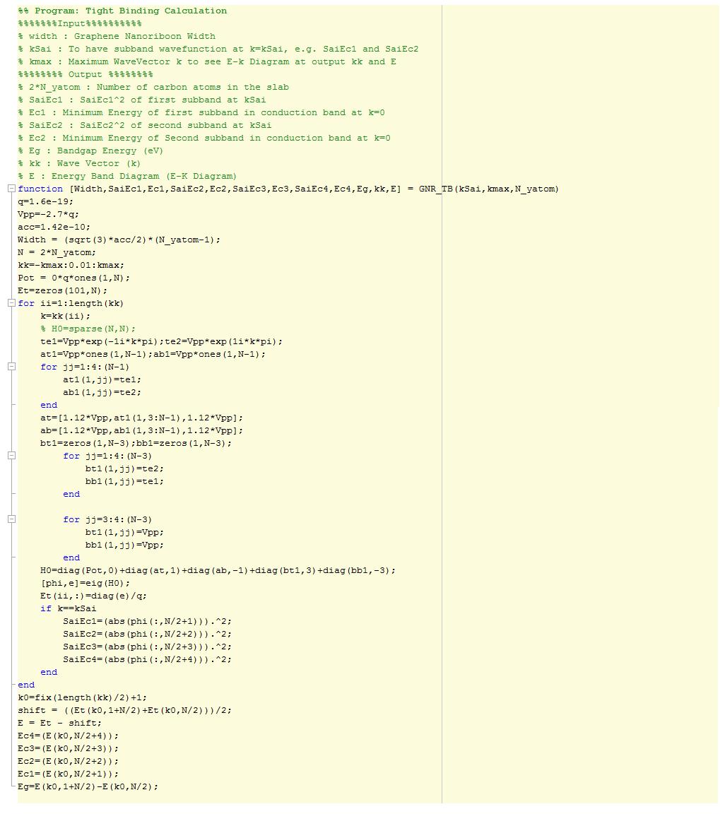
136 Functions: 120

137 121

138 122

139 123

140 124
141 125


142 126

143 127

144 128

145 129

146 130

147 APPENDIX B LETTER OF PERMISSION FOR FIGURE 2.3(c) 131
3-month progress Report
 3-month progress Report Graphene Devices and Circuits Supervisor Dr. P.A Childs Table of Content Abstract... 1 1. Introduction... 1 1.1 Graphene gold rush... 1 1.2 Properties of graphene... 3 1.3 Semiconductor
Device Performance Analysis of Graphene Nanoribbon Field-Effect Transistor with Rare- Earth Oxide (La 2 O 3 ) Based High-k Gate Dielectric
 Based High-k Gate Dielectric") Device Performance Analysis of Graphene Nanoribbon Field-Effect Transistor with Rare- Earth Oxide (La 2 O 3 ) Based High-k Gate Dielectric M. K. Bera 1, S. P. Pandey 2, A. K. Sharma 3, D. K. Tyagi 4, R.
Device Performance Analysis of Graphene Nanoribbon Field-Effect Transistor with Rare- Earth Oxide (La 2 O 3 ) Based High-k Gate Dielectric M. K. Bera 1, S. P. Pandey 2, A. K. Sharma 3, D. K. Tyagi 4, R.
Carbon based Nanoscale Electronics
 Carbon based Nanoscale Electronics 09 02 200802 2008 ME class Outline driving force for the carbon nanomaterial electronic properties of fullerene exploration of electronic carbon nanotube gold rush of
Evaluation of Electronic Characteristics of Double Gate Graphene Nanoribbon Field Effect Transistor for Wide Range of Temperatures
 Evaluation of Electronic Characteristics of Double Gate Graphene Nanoribbon Field Effect Transistor for Wide Range of Temperatures 1 Milad Abtin, 2 Ali Naderi 1 Department of electrical engineering, Masjed
Graphene. Tianyu Ye November 30th, 2011
 Graphene Tianyu Ye November 30th, 2011 Outline What is graphene? How to make graphene? (Exfoliation, Epitaxial, CVD) Is it graphene? (Identification methods) Transport properties; Other properties; Applications;
CITY UNIVERSITY OF HONG KONG. Theoretical Study of Electronic and Electrical Properties of Silicon Nanowires
 CITY UNIVERSITY OF HONG KONG Ë Theoretical Study of Electronic and Electrical Properties of Silicon Nanowires u Ä öä ªqk u{ Submitted to Department of Physics and Materials Science gkö y in Partial Fulfillment
GRAPHENE NANORIBBONS Nahid Shayesteh,
 USC Department of Physics Graduate Seminar 1 GRAPHENE NANORIBBONS Nahid Shayesteh, Outlines 2 Carbon based material Discovery and innovation of graphen Graphene nanoribbons structure Application of Graphene
EN2912C: Future Directions in Computing Lecture 08: Overview of Near-Term Emerging Computing Technologies
 EN2912C: Future Directions in Computing Lecture 08: Overview of Near-Term Emerging Computing Technologies Prof. Sherief Reda Division of Engineering Brown University Fall 2008 1 Near-term emerging computing
Graphene films on silicon carbide (SiC) wafers supplied by Nitride Crystals, Inc.
 wafers supplied by Nitride Crystals, Inc.") 9702 Gayton Road, Suite 320, Richmond, VA 23238, USA Phone: +1 (804) 709-6696 info@nitride-crystals.com www.nitride-crystals.com Graphene films on silicon carbide (SiC) wafers supplied by Nitride Crystals,
9702 Gayton Road, Suite 320, Richmond, VA 23238, USA Phone: +1 (804) 709-6696 info@nitride-crystals.com www.nitride-crystals.com Graphene films on silicon carbide (SiC) wafers supplied by Nitride Crystals,
MSE 310/ECE 340: Electrical Properties of Materials Fall 2014 Department of Materials Science and Engineering Boise State University
 MSE 310/ECE 340: Electrical Properties of Materials Fall 2014 Department of Materials Science and Engineering Boise State University Practice Final Exam 1 Read the questions carefully Label all figures
Graphene and Carbon Nanotubes
 Graphene and Carbon Nanotubes 1 atom thick films of graphite atomic chicken wire Novoselov et al - Science 306, 666 (004) 100μm Geim s group at Manchester Novoselov et al - Nature 438, 197 (005) Kim-Stormer
Impact of disorder and topology in two dimensional systems at low carrier densities
 Impact of disorder and topology in two dimensional systems at low carrier densities A Thesis Submitted For the Degree of Doctor of Philosophy in the Faculty of Science by Mohammed Ali Aamir Department
Initial Stages of Growth of Organic Semiconductors on Graphene
 Initial Stages of Growth of Organic Semiconductors on Graphene Presented by: Manisha Chhikara Supervisor: Prof. Dr. Gvido Bratina University of Nova Gorica Outline Introduction to Graphene Fabrication
(a) (b) Supplementary Figure 1. (a) (b) (a) Supplementary Figure 2. (a) (b) (c) (d) (e)
 (b) Supplementary Figure 1. (a) (b) (a) Supplementary Figure 2. (a) (b) (c) (d) (e)") (a) (b) Supplementary Figure 1. (a) An AFM image of the device after the formation of the contact electrodes and the top gate dielectric Al 2 O 3. (b) A line scan performed along the white dashed line
(a) (b) Supplementary Figure 1. (a) An AFM image of the device after the formation of the contact electrodes and the top gate dielectric Al 2 O 3. (b) A line scan performed along the white dashed line
CHAPTER 5 EFFECT OF GATE ELECTRODE WORK FUNCTION VARIATION ON DC AND AC PARAMETERS IN CONVENTIONAL AND JUNCTIONLESS FINFETS
 98 CHAPTER 5 EFFECT OF GATE ELECTRODE WORK FUNCTION VARIATION ON DC AND AC PARAMETERS IN CONVENTIONAL AND JUNCTIONLESS FINFETS In this chapter, the effect of gate electrode work function variation on DC
An Extended Hückel Theory based Atomistic Model for Graphene Nanoelectronics
 Journal of Computational Electronics X: YYY-ZZZ,? 6 Springer Science Business Media, Inc. Manufactured in The Netherlands An Extended Hückel Theory based Atomistic Model for Graphene Nanoelectronics HASSAN
Graphene transistor. Seminar I a. Mentor: doc. dr. Tomaž Rejec. April Abstract
 Graphene transistor Seminar I a Jan Srpčič Mentor: doc. dr. Tomaž Rejec April 2015 Abstract The topic of this seminar is graphene and its possible applications in the field of electronics, most notably
Supplementary Figure 1 Experimental setup for crystal growth. Schematic drawing of the experimental setup for C 8 -BTBT crystal growth.
 Supplementary Figure 1 Experimental setup for crystal growth. Schematic drawing of the experimental setup for C 8 -BTBT crystal growth. Supplementary Figure 2 AFM study of the C 8 -BTBT crystal growth
SUPPLEMENTARY INFORMATION
 SUPPLEMENTARY INFORMATION DOI: 10.1038/NNANO.2011.138 Graphene Nanoribbons with Smooth Edges as Quantum Wires Xinran Wang, Yijian Ouyang, Liying Jiao, Hailiang Wang, Liming Xie, Justin Wu, Jing Guo, and
Surfaces, Interfaces, and Layered Devices
 Surfaces, Interfaces, and Layered Devices Building blocks for nanodevices! W. Pauli: God made solids, but surfaces were the work of Devil. Surfaces and Interfaces 1 Interface between a crystal and vacuum
NiCl2 Solution concentration. Etching Duration. Aspect ratio. Experiment Atmosphere Temperature. Length(µm) Width (nm) Ar:H2=9:1, 150Pa
 Width (nm) Ar:H2=9:1, 150Pa") Experiment Atmosphere Temperature #1 # 2 # 3 # 4 # 5 # 6 # 7 # 8 # 9 # 10 Ar:H2=9:1, 150Pa Ar:H2=9:1, 150Pa Ar:H2=9:1, 150Pa Ar:H2=9:1, 150Pa Ar:H2=9:1, 150Pa Ar:H2=9:1, 150Pa Ar:H2=9:1, 150Pa Ar:H2=9:1,
Experiment Atmosphere Temperature #1 # 2 # 3 # 4 # 5 # 6 # 7 # 8 # 9 # 10 Ar:H2=9:1, 150Pa Ar:H2=9:1, 150Pa Ar:H2=9:1, 150Pa Ar:H2=9:1, 150Pa Ar:H2=9:1, 150Pa Ar:H2=9:1, 150Pa Ar:H2=9:1, 150Pa Ar:H2=9:1,
Black phosphorus: A new bandgap tuning knob
 Black phosphorus: A new bandgap tuning knob Rafael Roldán and Andres Castellanos-Gomez Modern electronics rely on devices whose functionality can be adjusted by the end-user with an external knob. A new
Review of Semiconductor Physics. Lecture 3 4 Dr. Tayab Din Memon
 Review of Semiconductor Physics Lecture 3 4 Dr. Tayab Din Memon 1 Electronic Materials The goal of electronic materials is to generate and control the flow of an electrical current. Electronic materials
Understanding the effect of n-type and p-type doping in the channel of graphene nanoribbon transistor
 Bull. Mater. Sci., Vol. 39, No. 5, September 2016, pp. 1303 1309. DOI 10.1007/s12034-016-1277-9 c Indian Academy of Sciences. Understanding the effect of n-type and p-type doping in the channel of graphene
Modeling and Performance analysis of Metallic CNT Interconnects for VLSI Applications
 IOSR Journal of Electronics and Communication Engineering (IOSR-JECE) e-issn: 2278-2834, p- ISSN: 2278-8735. Volume 4, Issue 6 (Jan. - Feb. 2013), PP 32-36 Modeling and Performance analysis of Metallic
Electronics with 2D Crystals: Scaling extender, or harbinger of new functions?
 Electronics with 2D Crystals: Scaling extender, or harbinger of new functions? 1 st Workshop on Data Abundant Systems Technology Stanford, April 2014 Debdeep Jena (djena@nd.edu) Electrical Engineering,
Available online at ScienceDirect. Procedia Materials Science 11 (2015 )
") Available online at www.sciencedirect.com ScienceDirect Procedia Materials Science 11 (2015 ) 287 292 5th International Biennial Conference on Ultrafine Grained and Nanostructured Materials, UFGNSM15 Tunneling
Available online at www.sciencedirect.com ScienceDirect Procedia Materials Science 11 (2015 ) 287 292 5th International Biennial Conference on Ultrafine Grained and Nanostructured Materials, UFGNSM15 Tunneling
OMEN an atomistic and full-band quantum transport simulator for post-cmos nanodevices
 Purdue University Purdue e-pubs Other Nanotechnology Publications Birck Nanotechnology Center 8-18-28 OMEN an atomistic and full-band quantum transport simulator for post-cmos nanodevices Mathieu Luisier
GRAPHENE NANORIBBONS Nahid Shayesteh,
 USC Department of Physics Graduate Seminar GRAPHENE NANORIBBONS Nahid Shayesteh, Outlines 2 Carbon based material Discovery and innovation of graphen Graphene nanoribbons structure and... FUNCTIONS 3 Carbon-based
A Numerical Study of Scaling Issues for Schottky Barrier Carbon Nanotube Transistors
 A Numerical Study of Scaling Issues for Schottky Barrier Carbon Nanotube Transistors Jing Guo, Supriyo Datta and Mark Lundstrom School of Electrical and Computer Engineering, Purdue University, West Lafayette,
Lectures Graphene and
 Lectures 15-16 Graphene and carbon nanotubes Graphene is atomically thin crystal of carbon which is stronger than steel but flexible, is transparent for light, and conducts electricity (gapless semiconductor).
Available online at ScienceDirect. Procedia Materials Science 11 (2015 )
") Available online at www.sciencedirect.com ScienceDirect Procedia Materials Science 11 (2015 ) 407 411 5th International Biennial Conference on Ultrafine Grained and Nanostructured Materials, FGNSM15 Simulation
Available online at www.sciencedirect.com ScienceDirect Procedia Materials Science 11 (2015 ) 407 411 5th International Biennial Conference on Ultrafine Grained and Nanostructured Materials, FGNSM15 Simulation
GRAPHENE the first 2D crystal lattice
 GRAPHENE the first 2D crystal lattice dimensionality of carbon diamond, graphite GRAPHENE realized in 2004 (Novoselov, Science 306, 2004) carbon nanotubes fullerenes, buckyballs what s so special about
Overview. Carbon in all its forms. Background & Discovery Fabrication. Important properties. Summary & References. Overview of current research
 Graphene Prepared for Solid State Physics II Pr Dagotto Spring 2009 Laurene Tetard 03/23/09 Overview Carbon in all its forms Background & Discovery Fabrication Important properties Overview of current
Nanocarbon Technology for Development of Innovative Devices
 Nanocarbon Technology for Development of Innovative Devices Shintaro Sato Daiyu Kondo Shinichi Hirose Junichi Yamaguchi Graphene, a one-atom-thick honeycomb lattice made of carbon, and a carbon nanotube,
1. Nanotechnology & nanomaterials -- Functional nanomaterials enabled by nanotechnologies.
 Novel Nano-Engineered Semiconductors for Possible Photon Sources and Detectors NAI-CHANG YEH Department of Physics, California Institute of Technology 1. Nanotechnology & nanomaterials -- Functional nanomaterials
Introduction to Nanotechnology Chapter 5 Carbon Nanostructures Lecture 1
 Introduction to Nanotechnology Chapter 5 Carbon Nanostructures Lecture 1 ChiiDong Chen Institute of Physics, Academia Sinica chiidong@phys.sinica.edu.tw 02 27896766 Section 5.2.1 Nature of the Carbon Bond
Supplementary Figure S1. AFM images of GraNRs grown with standard growth process. Each of these pictures show GraNRs prepared independently,
 Supplementary Figure S1. AFM images of GraNRs grown with standard growth process. Each of these pictures show GraNRs prepared independently, suggesting that the results is reproducible. Supplementary Figure
Self-study problems and questions Processing and Device Technology, FFF110/FYSD13
 Self-study problems and questions Processing and Device Technology, FFF110/FYSD13 Version 2016_01 In addition to the problems discussed at the seminars and at the lectures, you can use this set of problems
Indium arsenide quantum wire trigate metal oxide semiconductor field effect transistor
 JOURNAL OF APPLIED PHYSICS 99, 054503 2006 Indium arsenide quantum wire trigate metal oxide semiconductor field effect transistor M. J. Gilbert a and D. K. Ferry Department of Electrical Engineering and
Monolayer Semiconductors
 Monolayer Semiconductors Gilbert Arias California State University San Bernardino University of Washington INT REU, 2013 Advisor: Xiaodong Xu (Dated: August 24, 2013) Abstract Silicon may be unable to
Introduction to Nanotechnology Chapter 5 Carbon Nanostructures Lecture 1
 Introduction to Nanotechnology Chapter 5 Carbon Nanostructures Lecture 1 ChiiDong Chen Institute of Physics, Academia Sinica chiidong@phys.sinica.edu.tw 02 27896766 Carbon contains 6 electrons: (1s) 2,
ARCHITECTURE AND CAD FOR CARBON NANOMATERIAL INTEGRATED CIRCUITS SCOTT ERICK CHILSTEDT THESIS
 ARCHITECTURE AND CAD FOR CARBON NANOMATERIAL INTEGRATED CIRCUITS BY SCOTT ERICK CHILSTEDT THESIS Submitted in partial fulfillment of the requirements for the degree of Master of Science in Electrical and
Graphene Novel Material for Nanoelectronics
 Graphene Novel Material for Nanoelectronics Shintaro Sato Naoki Harada Daiyu Kondo Mari Ohfuchi (Manuscript received May 12, 2009) Graphene is a flat monolayer of carbon atoms with a two-dimensional honeycomb
CMPEN 411 VLSI Digital Circuits. Lecture 03: MOS Transistor
 CMPEN 411 VLSI Digital Circuits Lecture 03: MOS Transistor Kyusun Choi [Adapted from Rabaey s Digital Integrated Circuits, Second Edition, 2003 J. Rabaey, A. Chandrakasan, B. Nikolic] CMPEN 411 L03 S.1
CMOS Scaling. Two motivations to scale down. Faster transistors, both digital and analog. To pack more functionality per area. Lower the cost!
 Two motivations to scale down CMOS Scaling Faster transistors, both digital and analog To pack more functionality per area. Lower the cost! (which makes (some) physical sense) Scale all dimensions and
Carbon Nanotubes in Interconnect Applications
 Carbon Nanotubes in Interconnect Applications Page 1 What are Carbon Nanotubes? What are they good for? Why are we interested in them? - Interconnects of the future? Comparison of electrical properties
Wafer-scale fabrication of graphene
 Wafer-scale fabrication of graphene Sten Vollebregt, MSc Delft University of Technology, Delft Institute of Mircosystems and Nanotechnology Delft University of Technology Challenge the future Delft University
The Critical Role of Quantum Capacitance in Compact Modeling of Nano-Scaled and Nanoelectronic Devices
 The Critical Role of Quantum Capacitance in Compact Modeling of Nano-Scaled and Nanoelectronic Devices Zhiping Yu and Jinyu Zhang Institute of Microelectronics Tsinghua University, Beijing, China yuzhip@tsinghua.edu.cn
On the possibility of tunable-gap bilayer graphene FET
 On the possibility of tunable-gap bilayer graphene FET 1 arxiv:0810.0128v1 [cond-mat.mes-hall] 1 Oct 2008 Gianluca Fiori, Giuseppe Iannaccone Dipartimento di Ingegneria dell Informazione : Elettronica,
Graphene based FETs. Raghav Gupta ( )
") 1 Graphene based FETs Raghav Gupta (10327553) Abstract The extraordinary electronic properties along with excellent optical, mechanical, thermodynamic properties have led to a lot of interest in its possible
1 Graphene based FETs Raghav Gupta (10327553) Abstract The extraordinary electronic properties along with excellent optical, mechanical, thermodynamic properties have led to a lot of interest in its possible
Emerging Interconnect Technologies for CMOS and beyond-cmos Circuits
 Emerging Interconnect Technologies for CMOS and beyond-cmos Circuits Sou-Chi Chang, Rouhollah M. Iraei Vachan Kumar, Ahmet Ceyhan and Azad Naeemi School of Electrical & Computer Engineering Georgia Institute
Dissipative Transport in Rough Edge Graphene Nanoribbon. Tunnel Transistors
 Dissipative Transport in Rough Edge Graphene Nanoribbon Tunnel Transistors Youngki Yoon and Sayeef Salahuddin Department of Electrical Engineering and Computer Sciences, University of California, Berkeley,
Fabrication Technology, Part I
 EEL5225: Principles of MEMS Transducers (Fall 2004) Fabrication Technology, Part I Agenda: Microfabrication Overview Basic semiconductor devices Materials Key processes Oxidation Thin-film Deposition Reading:
Performance Comparison of Graphene Nanoribbon FETs. with Schottky Contacts and Doped Reservoirs
 Performance Comparison of Graphene Nanoribbon FETs with Schottky Contacts and Doped Reservoirs Youngki Yoon 1,a, Gianluca Fiori 2,b, Seokmin Hong 1, Giuseppe Iannaccone 2, and Jing Guo 1 1 Department of
Electric Field-Dependent Charge-Carrier Velocity in Semiconducting Carbon. Nanotubes. Yung-Fu Chen and M. S. Fuhrer
 Electric Field-Dependent Charge-Carrier Velocity in Semiconducting Carbon Nanotubes Yung-Fu Chen and M. S. Fuhrer Department of Physics and Center for Superconductivity Research, University of Maryland,
MOS CAPACITOR AND MOSFET
 EE336 Semiconductor Devices 1 MOS CAPACITOR AND MOSFET Dr. Mohammed M. Farag Ideal MOS Capacitor Semiconductor Devices Physics and Technology Chapter 5 EE336 Semiconductor Devices 2 MOS Capacitor Structure
From nanophysics research labs to cell phones. Dr. András Halbritter Department of Physics associate professor
 From nanophysics research labs to cell phones Dr. András Halbritter Department of Physics associate professor Curriculum Vitae Birth: 1976. High-school graduation: 1994. Master degree: 1999. PhD: 2003.
Computational Model of Edge Effects in Graphene Nanoribbon Transistors
 Nano Res (2008) 1: 395 402 DOI 10.1007/s12274-008-8039-y Research Article 00395 Computational Model of Edge Effects in Graphene Nanoribbon Transistors Pei Zhao 1, Mihir Choudhury 2, Kartik Mohanram 2,
1 Name: Student number: DEPARTMENT OF PHYSICS AND PHYSICAL OCEANOGRAPHY MEMORIAL UNIVERSITY OF NEWFOUNDLAND. Fall :00-11:00
 1 Name: DEPARTMENT OF PHYSICS AND PHYSICAL OCEANOGRAPHY MEMORIAL UNIVERSITY OF NEWFOUNDLAND Final Exam Physics 3000 December 11, 2012 Fall 2012 9:00-11:00 INSTRUCTIONS: 1. Answer all seven (7) questions.
OPTI510R: Photonics. Khanh Kieu College of Optical Sciences, University of Arizona Meinel building R.626
 OPTI510R: Photonics Khanh Kieu College of Optical Sciences, University of Arizona kkieu@optics.arizona.edu Meinel building R.626 Announcements HW#3 is assigned due Feb. 20 st Mid-term exam Feb 27, 2PM
Spatially resolving density-dependent screening around a single charged atom in graphene
 Supplementary Information for Spatially resolving density-dependent screening around a single charged atom in graphene Dillon Wong, Fabiano Corsetti, Yang Wang, Victor W. Brar, Hsin-Zon Tsai, Qiong Wu,
Optimizing Graphene Morphology on SiC(0001)
") Optimizing Graphene Morphology on SiC(0001) James B. Hannon Rudolf M. Tromp Graphene sheets Graphene sheets can be formed into 0D,1D, 2D, and 3D structures Chemically inert Intrinsically high carrier mobility
Optimizing Graphene Morphology on SiC(0001) James B. Hannon Rudolf M. Tromp Graphene sheets Graphene sheets can be formed into 0D,1D, 2D, and 3D structures Chemically inert Intrinsically high carrier mobility
Transient Photocurrent Measurements of Graphene Related Materials
 Transient Photocurrent Measurements of Graphene Related Materials P. Srinivasa Rao Mentor: Prof. dr. Gvido Bratina Laboratory of Organic Matter Physics University of Nova Gorica 1 Contents: 1. Electrical
Graphene Fundamentals and Emergent Applications
 Graphene Fundamentals and Emergent Applications Jamie H. Warner Department of Materials University of Oxford Oxford, UK Franziska Schaffel Department of Materials University of Oxford Oxford, UK Alicja
Graphite, graphene and relativistic electrons
 Graphite, graphene and relativistic electrons Introduction Physics of E. graphene Y. Andrei Experiments Rutgers University Transport electric field effect Quantum Hall Effect chiral fermions STM Dirac
Graphene - most two-dimensional system imaginable
 Graphene - most two-dimensional system imaginable A suspended sheet of pure graphene a plane layer of C atoms bonded together in a honeycomb lattice is the most two-dimensional system imaginable. A.J.
Nanostructures. Lecture 13 OUTLINE
 Nanostructures MTX9100 Nanomaterials Lecture 13 OUTLINE -What is quantum confinement? - How can zero-dimensional materials be used? -What are one dimensional structures? -Why does graphene attract so much
Semiconductor Physics Problems 2015
 Semiconductor Physics Problems 2015 Page and figure numbers refer to Semiconductor Devices Physics and Technology, 3rd edition, by SM Sze and M-K Lee 1. The purest semiconductor crystals it is possible
Lecture 0: Introduction
 Lecture 0: Introduction Introduction q Integrated circuits: many transistors on one chip q Very Large Scale Integration (VLSI): bucketloads! q Complementary Metal Oxide Semiconductor Fast, cheap, low power
CVD growth of Graphene. SPE ACCE presentation Carter Kittrell James M. Tour group September 9 to 11, 2014
 CVD growth of Graphene SPE ACCE presentation Carter Kittrell James M. Tour group September 9 to 11, 2014 Graphene zigzag armchair History 1500: Pencil-Is it made of lead? 1789: Graphite 1987: The first
Nanoelectronics. Topics
 Nanoelectronics Topics Moore s Law Inorganic nanoelectronic devices Resonant tunneling Quantum dots Single electron transistors Motivation for molecular electronics The review article Overview of Nanoelectronic
SiC Graphene Suitable For Quantum Hall Resistance Metrology.
 SiC Graphene Suitable For Quantum Hall Resistance Metrology. Samuel Lara-Avila 1, Alexei Kalaboukhov 1, Sara Paolillo, Mikael Syväjärvi 3, Rositza Yakimova 3, Vladimir Fal'ko 4, Alexander Tzalenchuk 5,
EE130: Integrated Circuit Devices
 EE130: Integrated Circuit Devices (online at http://webcast.berkeley.edu) Instructor: Prof. Tsu-Jae King (tking@eecs.berkeley.edu) TA s: Marie Eyoum (meyoum@eecs.berkeley.edu) Alvaro Padilla (apadilla@eecs.berkeley.edu)
Supporting Information. by Hexagonal Boron Nitride
 Supporting Information High Velocity Saturation in Graphene Encapsulated by Hexagonal Boron Nitride Megan A. Yamoah 1,2,, Wenmin Yang 1,3, Eric Pop 4,5,6, David Goldhaber-Gordon 1 * 1 Department of Physics,
Graphene FETs EE439 FINAL PROJECT. Yiwen Meng Su Ai
 Graphene FETs EE439 FINAL PROJECT Yiwen Meng Su Ai Introduction What is Graphene? An atomic-scale honeycomb lattice made of carbon atoms Before 2004, Hypothetical Carbon Structure Until 2004, physicists
Carbon Nanotube Ring Oscillator for Detecting Ionized Radiation
 Journal of Materials Science and Engineering A 6 (7-8) (2016) 205-212 doi: 10.17265/2161-6213/2016.7-8.003 D DAVID PUBLISHING Carbon Nanotube Ring Oscillator for Detecting Ionized Radiation Yaser Mohammadi
Classification of Solids
 Classification of Solids Classification by conductivity, which is related to the band structure: (Filled bands are shown dark; D(E) = Density of states) Class Electron Density Density of States D(E) Examples
Projected Performance Advantage of Multilayer Graphene Nanoribbon as Transistor Channel Material
 Projected Performance Advantage of Multilayer Graphene Nanoribbon as Transistor Channel Material Yijian Ouyang 1, Hongjie Dai 2, and Jing Guo 1 1 Department of Electrical and Computer Engineering, University
Performance Analysis of Ultra-Scaled InAs HEMTs
 Purdue University Purdue e-pubs Birck and NCN Publications Birck Nanotechnology Center 2009 Performance Analysis of Ultra-Scaled InAs HEMTs Neerav Kharche Birck Nanotechnology Center and Purdue University,
SUPPLEMENTARY INFORMATION
 SUPPLEMENTARY INFORMATION Facile Synthesis of High Quality Graphene Nanoribbons Liying Jiao, Xinran Wang, Georgi Diankov, Hailiang Wang & Hongjie Dai* Supplementary Information 1. Photograph of graphene
Electro - Principles I
 Electro - Principles I Page 10-1 Atomic Theory It is necessary to know what goes on at the atomic level of a semiconductor so the characteristics of the semiconductor can be understood. In many cases a
Review Energy Bands Carrier Density & Mobility Carrier Transport Generation and Recombination
 Review Energy Bands Carrier Density & Mobility Carrier Transport Generation and Recombination The Metal-Semiconductor Junction: Review Energy band diagram of the metal and the semiconductor before (a)
Digital Electronics Part II - Circuits
 Digital Electronics Part - Circuits Dr.. J. Wassell Gates from Transistors ntroduction Logic circuits are non-linear, consequently we will introduce a graphical technique for analysing such circuits The
Exceptional ballistic transport in epigraphene. Walt de Heer Georgia Institute of Technology
 Exceptional ballistic transport in epigraphene Walt de Heer Georgia Institute of Technology Program Objective First formulated in 2001 and patented in 2003, our objective is to develop nanoelectronics
Semiconductor Physics fall 2012 problems
 Semiconductor Physics fall 2012 problems 1. An n-type sample of silicon has a uniform density N D = 10 16 atoms cm -3 of arsenic, and a p-type silicon sample has N A = 10 15 atoms cm -3 of boron. For each
Projected Performance Advantage of Multilayer Graphene Nanoribbons as a Transistor Channel Material
 1Nano Res (2010) 3: 8 15 DOI 10.1007/s12274-010-1002-8 Research Article Projected Performance Advantage of Multilayer Graphene Nanoribbons as a Transistor Channel Material Yijian Ouyang 1 ( ), Hongjie
Graphene Devices, Interconnect and Circuits Challenges and Opportunities
 Graphene Devices, Interconnect and Circuits Challenges and Opportunities Mircea R. Stan, Dincer Unluer, Avik Ghosh, Frank Tseng Univ. of Virginia, ECE Dept., Charlottesville, VA 22904 {mircea,du7x,ag7rq,ft8e}@virginia.edu
Lecture 5: CMOS Transistor Theory
 Lecture 5: CMOS Transistor Theory Slides courtesy of Deming Chen Slides based on the initial set from David Harris CMOS VLSI Design Outline q q q q q q q Introduction MOS Capacitor nmos I-V Characteristics
Supporting information
 Supporting information Design, Modeling and Fabrication of CVD Grown MoS 2 Circuits with E-Mode FETs for Large-Area Electronics Lili Yu 1*, Dina El-Damak 1*, Ujwal Radhakrishna 1, Xi Ling 1, Ahmad Zubair
MOS Transistor Theory
 CHAPTER 3 MOS Transistor Theory Outline 2 1. Introduction 2. Ideal I-V Characteristics 3. Nonideal I-V Effects 4. C-V Characteristics 5. DC Transfer Characteristics 6. Switch-level RC Delay Models MOS
Performance Analysis of Multilayer Graphene Nano Ribbon as on chip Interconnect.
 Performance Analysis of Multilayer Graphene Nano Ribbon as on chip Interconnect. G.Chitra 1, P.Murugeswari 2 1 (Post Graduate Student, VLSI Design, Theni Kammavar Sangam College of Technology, Theni, India)
Electrical Transport Measurements Show Intrinsic Doping and Hysteresis in Graphene p-n Junction Devices
 Electrical Transport Measurements Show Intrinsic Doping and Hysteresis in Graphene p-n Junction Devices Garrett Plunkett Department of Physics Oregon State University June 6, 017 Advisor: Dr. Matthew Graham
Research Article Analyses of Short Channel Effects of Single-Gate and Double-Gate Graphene Nanoribbon Field Effect Transistors
 Materials Volume 6, Article ID 84469, 8 pages http://dx.doi.org/.55/6/84469 Research Article Analyses of Short Channel Effects of Single-Gate and Double-Gate Graphene Nanoribbon Field Effect Transistors
ESE 570: Digital Integrated Circuits and VLSI Fundamentals
 ESE 570: Digital Integrated Circuits and VLSI Fundamentals Lec 4: January 23, 2018 MOS Transistor Theory, MOS Model Penn ESE 570 Spring 2018 Khanna Lecture Outline! CMOS Process Enhancements! Semiconductor
Supplementary Figure 1. Selected area electron diffraction (SAED) of bilayer graphene and tblg. (a) AB
 of bilayer graphene and tblg. (a) AB") Supplementary Figure 1. Selected area electron diffraction (SAED) of bilayer graphene and tblg. (a) AB stacked bilayer graphene (b), (c), (d), (e), and (f) are twisted bilayer graphene with twist angle
Supplementary Figure 1. Selected area electron diffraction (SAED) of bilayer graphene and tblg. (a) AB stacked bilayer graphene (b), (c), (d), (e), and (f) are twisted bilayer graphene with twist angle
Stretching the Barriers An analysis of MOSFET Scaling. Presenters (in order) Zeinab Mousavi Stephanie Teich-McGoldrick Aseem Jain Jaspreet Wadhwa
 Zeinab Mousavi Stephanie Teich-McGoldrick Aseem Jain Jaspreet Wadhwa") Stretching the Barriers An analysis of MOSFET Scaling Presenters (in order) Zeinab Mousavi Stephanie Teich-McGoldrick Aseem Jain Jaspreet Wadhwa Why Small? Higher Current Lower Gate Capacitance Higher
Stretching the Barriers An analysis of MOSFET Scaling Presenters (in order) Zeinab Mousavi Stephanie Teich-McGoldrick Aseem Jain Jaspreet Wadhwa Why Small? Higher Current Lower Gate Capacitance Higher
Metallic: 2n 1. +n 2. =3q Armchair structure always metallic = 2
 Properties of CNT d = 2.46 n 2 2 1 + n1n2 + n2 2π Metallic: 2n 1 +n 2 =3q Armchair structure always metallic a) Graphite Valence(π) and Conduction(π*) states touch at six points(fermi points) Carbon Nanotube:
Section 12: Intro to Devices
 Section 12: Intro to Devices Extensive reading materials on reserve, including Robert F. Pierret, Semiconductor Device Fundamentals EE143 Ali Javey Bond Model of Electrons and Holes Si Si Si Si Si Si Si
Drift-diffusion model for single layer transition metal dichalcogenide field-effect transistors
 Drift-diffusion model for single layer transition metal dichalcogenide field-effect transistors David Jiménez Departament d'enginyeria Electrònica, Escola d'enginyeria, Universitat Autònoma de Barcelona,