Graphene - most two-dimensional system imaginable
|
|
|
- Shonda Powers
- 6 years ago
- Views:
Transcription
, C nanotubes (a graphene sheet rolled into a cylinder) and")
1 Graphene - most two-dimensional system imaginable A suspended sheet of pure graphene a plane layer of C atoms bonded together in a honeycomb lattice is the most two-dimensional system imaginable. A.J. Leggett Such sheets have long been known to exist in disguised forms in graphite (many graphene sheets stacked on top of one another), C nanotubes (a graphene sheet rolled into a cylinder) and fullerenes (buckyballs), which are small areas of a graphene sheet sewn together to form an approximately spherical surface. Until 2004, it was generally believed (a) that an extended graphene sheet would not be stable against the effects of thermal and other fluctuations, and (b) that even if they were stable, it would be impossible to isolate them so that their properties could be systematically studied. Modified from: Dr. Chris Ewels, Inst. of Materials
 demonstrated that both these beliefs were false: they created single graphene sheets by peeling them off a graphite substrate using scotch tape, and characterized them")
2 In 2004, André Geim et al. (University of Manchester, UK) demonstrated that both these beliefs were false: they created single graphene sheets by peeling them off a graphite substrate using scotch tape, and characterized them as indeed single-sheet by simple optical microscopy on top of a SiO 2 substrate. Now it is done mostly by Raman spectroscopy. Subsequently it was found that small graphene sheets do not need to rest on substrates but can be freely suspended from a scaffolding; furthermore, bilayer and multilayer sheets can be prepared and characterized. As a result of these developments, the number of papers on graphene published in the last few years exceeds The Nobel Prize in Physics 2010 Andre Geim Konstantin Novoselov Graphene is a very promising material both for applications and fundamental research.
 arxiv:0705.")
3 The trick: Finding the Graphene Using correct substrate And correct light frequency Interference effect makes monolayers show up in ordinary optical microscope Graphene Blake et al (2007) arxiv: SiO Si
![What is graphene? Imagine a piece of paper but a million times thinner. This is how thick graphene is. Imagine a material stronger than diamond. This is how strong graphene is [in the plane].](/docs-images/75/72940424/images/4-0.jpg "Imagine a material more conducting than copper. This is how conductive graphene is.")
4 What is graphene? Imagine a piece of paper but a million times thinner. This is how thick graphene is. Imagine a material stronger than diamond. This is how strong graphene is [in the plane]. Imagine a material more conducting than copper. This is how conductive graphene is. Imagine a machine that can test the same physics that scientists test in, say, CERN, but small enough to stand on top of your table. Graphene allows this to happen. Having such a material in hand, one can easily think of many useful things that can eventually come out. As concerns new physics, no one doubts about it already...'' From a recently interview with Andre Geim.

5 Carbon is the materia prima for life and the basis of all organic chemistry. Because of the flexibility of its bonding, carbon-based systems show an unlimited number of different structures with an equally large variety of physical properties. Graphene is a honeycomb lattice of carbon atoms. Carbon nanotubes are rolled-up cylinders of graphene Graphite can be viewed as a stack of graphene layers. Fullerenes C 60 are molecules consisting of wrapped graphene by the introduction of pentagons on the hexagonal lattice. From Castro Neto et al, 2009


6 Crystal structure The electronic structure of an isolated C atom is (1s) 2 (2s) 2 (2p) 4 ; in a solid-state environment the 1s electrons remain more or less inert, but the 2s and 2p electrons hybridize. One possible result is four sp 3 orbitals, which naturally tend to establish a tetrahedral bonding pattern that soaks up all the valence electrons: this is precisely what happens in the best known solid form of C, namely diamond, which is a very good insulator (band gap about 5 ev). An alternative possibility is to form three sp 2 orbitals, leaving over a more or less pure p- orbital. In that case the natural tendency is for the sp 2 orbitals to arrange themselves in a plane at 120 o angles, and the lattice thus formed is the honeycomb lattice.

7 Band structure Lattice structure of graphene, made out of two interpenetrating triangular lattices a 1 and a 2 are the lattice unit vectors, and δ i are the nearest-neighbor vectors. Corresponding Brillouin zone.

8 Energy vanishes at the points K, K, and those equivalent to them The picture and derivations adapted from Castro Neto et al., Rev. Mod. Phys. 81, 109 (2009)
")

9 Sketch of derivation (1) Wallace, Phys. Rev. 71, 622 (1947)
10 Sketch of derivation (2)
11 Conic (Dirac) points Let us put and expand the Hamiltonian in small Coefficient can be dropped Similarly It is suggestive to express the Hamiltonian describing conic points in the form - Pauli matrices The Hamiltonian is, from a formal point of view, exactly that of an ultra-relativistic (or mass-less) particle of spin 1/2 (such as the neutrino), with the velocity of light c replaced by the Fermi velocity v F, which is a factor 300 smaller.
12 Thus there arises the prospect, which excites a lot of people, of finding analogs to many phenomena predicted to occur in a solid-state context. Comment However, it should be remembered that the Dirac excitations near K are not the antiparticles of those near K ; rather it is the two possible combinations of the excitations near one Dirac point on the A and B sub-lattices, with energies respectively, which are one another s antiparticles. Eigenfunctions for the vicinity of the K-point Note that when q rotates once around the Dirac point, the phase of changes by, not by, as is characteristic for spin-1/2 particles.

13 Important parameters for conic spectrum Density of states at K-point: Since there are 2 Dirac points How one can introduce effective mass? Doping shifts the Fermi level leading to creating a Fermi line. This definition provides the cyclotron effective mass.

.")
14 Klein tunneling Due to the chiral nature of their quasiparticles, quantum tunneling in these materials becomes highly anisotropic, qualitatively different from the case of normal, nonrelativistic electrons. Massless Dirac fermions in graphene allow a close realization of Klein s gedanken experiment - unimpeded penetration of relativistic particles through high and wide potential barriers. The paradox: When the barrier increases, transmission becomes perfect! Schematic diagrams of the spectrum of quasiparticles in single-layer graphene. The spectrum is linear at low Fermi energies (<1eV). The red and green curves emphasize the origin of the linear spectrum, which is the crossing between the energy bands associated with crystal sublattices A and B. The Fermi level (dotted lines) lies in the conduction band outside the barrier and the valence band inside it. The blue filling indicates occupied states.

15 Explanation: Absence of backscattering for Adapted from Beenakker, 2007 Because the magnitude v of the carrier velocity is independent of the energy, an electron moving along the field lines cannot be backscattered since that would require v = 0 at the turning point.
16 An electron-like excitation continue under the barrier as a hole-like one Momentum changes its sign, but the (group) velocity is conserved. As a result anisotropic scattering. Result for high energies : Under resonance conditions transparent (interference effects). the barrier becomes More significantly, however, the barrier always remains perfectly transparent for angles close to the normal incidence φ = 0. The latter is the feature unique to massless Dirac fermions and is directly related to the Klein paradox in QED.
 electrostatic potential profile U(x) along the cross-section of a).")
17 Klein tunneling is the mechanism for electrical conduction through the interface between p-doped and n-doped graphene. n-p-n junction in graphene a) cross-sectional view of the device. b) electrostatic potential profile U(x) along the cross-section of a). The combination of a positive voltage on the back gate and a negative voltage on the top gate produces a central p- doped region flanked by two n-doped regions. c) Optical image of the device. The barely visible graphene flake is outlined with a dashed line and the dielectric layer of PMMA appears as a blue shadow. (Huard et al., 2007)
18 Minimal conductance of graphene What happens with the conductance of graphene when the Fermi level reaches the conic point? Does it vanish or not? The conductance reaches a minimum corresponding to double value comparing to the value at the lowest quantum Hall plateau. Conductivity versus gate voltage

19 Minimal conductance of graphene The band structure of graphene has two valleys, which are decoupled in the case of a smooth edge. In a given valley the excitations have a two-component envelope wave function The two components of refer to the two sublattices in the two-dimensional honeycomb lattice of carbon atoms. Dirac equation: with the velocity of the massless excitations of charge and energy, the momentum operator,, the position, and a Pauli matrix. We choose the zero of energy such that the Fermi level is at. Boundary conditions: The transversal momenta are quantized as: Tworzydlo et al., 2006
20 Level quantization and quantum Hall Effect in graphene At a typical doping, electrons are degenerate at room temperature. In the absence of magnetic field the tight binding Hamiltonian close to Dirac points is In magnetic field one has to replace to get: We have to find eigenvalues of this Hamiltonian versus magnetic field B
21 Let us assume that and choose the Landau gauge It is also convenient to choose dimensionless variables Measuring lengths in units of, one gets The Hamiltonian can be rewritten as It is immediately seen that the energies are parameterized by the quantity
22 Trick: let us apply the Hamilton operator twice. We have Note that the operator is the Hamiltonian of a dimensionless Harmonic oscillator with eigenvalues Consequently, Quantum numbers n correspond to Landau levels, but they are not equidistant. The number of states per the Landau level corresponds to the number of flux quanta through the cell,
23 Experimental check: gated structures Manchester group
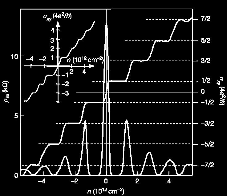
24 Room-temperature quantum Hall Effect in graphene At B=45 T the Fermi level is located between n=0 and 1 At T= 300 K, the plateaus are seen at B < 20 T
25 What I have not discussed. Bilayer graphene Epitaxial graphene and graphene stacks Surface states in graphene and graphene stacks Graphene nanoribbons Flexural Phonons, Elasticity, and Crumpling Disorder in Graphene: Ripples, topological lattice defects, impurity states, localized states near edges, cracks, and voids; vector potential and gauge field disorder, coupling to magnetic impurities Many-Body Effects: Electron-phonon interactions, electron-electron interactions, short-range interactions Mechanical properties Potential device applications: Single molecule gas detection, Graphene nanoribbons as ballistic and FET transistor devices and components for integrated circuits; Transparent conducting electrodes, Graphene biodevices, NEMSs, components of lasers, etc

26 100 GHz transistor from Wafer-Scale Epitaxial Graphene Cutoff frequency of 100 gigahertz for a gate length of 240 nanometers. The high-frequency performance of these epitaxial graphene transistors exceeds that of state-of-the-art silicon transistors of the same gate length. (A) Image of devices fabricated on a 2-inch graphene wafer and schematic cross-sectional view of a top-gated graphene FET. (B) The drain current, I D, of a graphene FET (gate length L G = 240 nm) as a function of gate voltage at drain bias of 1 V with the source electrode grounded. The device transconductance, gm, is shown on the right axis. (C) The drain current as a function of V D of a graphene FET (L G = 240 nm) for various gate voltages. (D) Measured small-signal current gain h 21 as a function of frequency f for a 240-nm-gate ( ) and a 550-nm-gate ( ) graphene FET at V D = 2.5 V. Cutoff frequencies, f T, were 53 and 100 GHz for the 550-nm and 240-nm devices, respectively. Ph. Avouris group, IBM
 substrate with graphene after high-temperature annealing in an argon atmosphere.")
27 Model device acting as a resistor standard T=300 mk Accuracy ca. 3x10⁻⁹ a, AFM images of the sample: large flat terraces on the surface of the Si-face of a 4H-SiC(0001) substrate with graphene after high-temperature annealing in an argon atmosphere. b, Graphene patterned in the nominally 2-μm-wide Hall bar configuration on top of the terraced substrate. c, Layout of a 7 7 mm 2 wafer with 20 patterned devices. Encircled are two devices with dimensions L = 11.6 µm and W = 2 µm (wire bonded) and L = 160 µm and W = 35 µm. The contact configuration for the smaller device is shown in the enlarged image. To visualize the Hall bar this optical micrograph was taken after oxygen plasma treatment, which formed the graphene pattern, but before the removal of resist. Nature Nanotechnology 5, (2010)
")


28 First graphene touch screen The process includes adhesion of polymer supports, copper etching (rinsing) and dry transferprinting on a target substrate. A wet-chemical doping can be carried out using a set-up similar to that used for etching. Sustains strain up to 6% Extremely promising for transparent electrodes Nature Nanotechnology (2010)

29 Example: Graphene Q-switched, tunable fiber laser Group by Ferrari, UK: preprint 2010 Graphene is used as a non-linear (saturated absorption) medium to create short optical pulses. The authors have succeeded to make 2 μs pulses, tunable between 1522 and 1555 nm with up to 40nJ energy. This is a simple and low-cost light source for metrology, environmental sensing and biomedical diagnostics. Studies of graphene is a very interesting and promising area, but a lot of things remains to be done to create graphene electronics.


30 Giant Faraday rotation Graphene turns the polarization by several degrees in modest magnetic fields. This opens pathways to use graphene in fast tunable ultrathin infrared magneto-optical devices. The polarization plane of the linearly polarized incoming beam is rotated by the Faraday angle θ after passing through graphene on a SiC substrate in a perpendicular magnetic field. Studies of graphene is a very interesting and promising area, but a lot of things remains to be done to create graphene electronics. Simultaneously, the polarization acquires a certain ellipticity. Crassee et al., Nature Physics
GRAPHENE the first 2D crystal lattice
 GRAPHENE the first 2D crystal lattice dimensionality of carbon diamond, graphite GRAPHENE realized in 2004 (Novoselov, Science 306, 2004) carbon nanotubes fullerenes, buckyballs what s so special about
Graphene. Tianyu Ye November 30th, 2011
 Graphene Tianyu Ye November 30th, 2011 Outline What is graphene? How to make graphene? (Exfoliation, Epitaxial, CVD) Is it graphene? (Identification methods) Transport properties; Other properties; Applications;
Carbon based Nanoscale Electronics
 Carbon based Nanoscale Electronics 09 02 200802 2008 ME class Outline driving force for the carbon nanomaterial electronic properties of fullerene exploration of electronic carbon nanotube gold rush of
Graphene The Search For Two Dimensions. Christopher Scott Friedline Arizona State University
 Graphene The Search For Two Dimensions Christopher Scott Friedline Arizona State University What Is Graphene? Single atomic layer of graphite arranged in a honeycomb crystal lattice Consists of sp 2 -bonded
3-month progress Report
 3-month progress Report Graphene Devices and Circuits Supervisor Dr. P.A Childs Table of Content Abstract... 1 1. Introduction... 1 1.1 Graphene gold rush... 1 1.2 Properties of graphene... 3 1.3 Semiconductor
SiC Graphene Suitable For Quantum Hall Resistance Metrology.
 SiC Graphene Suitable For Quantum Hall Resistance Metrology. Samuel Lara-Avila 1, Alexei Kalaboukhov 1, Sara Paolillo, Mikael Syväjärvi 3, Rositza Yakimova 3, Vladimir Fal'ko 4, Alexander Tzalenchuk 5,
Graphite, graphene and relativistic electrons
 Graphite, graphene and relativistic electrons Introduction Physics of E. graphene Y. Andrei Experiments Rutgers University Transport electric field effect Quantum Hall Effect chiral fermions STM Dirac
Black phosphorus: A new bandgap tuning knob
 Black phosphorus: A new bandgap tuning knob Rafael Roldán and Andres Castellanos-Gomez Modern electronics rely on devices whose functionality can be adjusted by the end-user with an external knob. A new
TRANSVERSE SPIN TRANSPORT IN GRAPHENE
 International Journal of Modern Physics B Vol. 23, Nos. 12 & 13 (2009) 2641 2646 World Scientific Publishing Company TRANSVERSE SPIN TRANSPORT IN GRAPHENE TARIQ M. G. MOHIUDDIN, A. A. ZHUKOV, D. C. ELIAS,
Electronic properties of graphene. Jean-Noël Fuchs Laboratoire de Physique des Solides Université Paris-Sud (Orsay)
") Electronic properties of graphene Jean-Noël Fuchs Laboratoire de Physique des Solides Université Paris-Sud (Orsay) Cargèse, September 2012 3 one-hour lectures in 2 x 1,5h on electronic properties of graphene
Electronic properties of graphene Jean-Noël Fuchs Laboratoire de Physique des Solides Université Paris-Sud (Orsay) Cargèse, September 2012 3 one-hour lectures in 2 x 1,5h on electronic properties of graphene
Graphene films on silicon carbide (SiC) wafers supplied by Nitride Crystals, Inc.
 wafers supplied by Nitride Crystals, Inc.") 9702 Gayton Road, Suite 320, Richmond, VA 23238, USA Phone: +1 (804) 709-6696 info@nitride-crystals.com www.nitride-crystals.com Graphene films on silicon carbide (SiC) wafers supplied by Nitride Crystals,
9702 Gayton Road, Suite 320, Richmond, VA 23238, USA Phone: +1 (804) 709-6696 info@nitride-crystals.com www.nitride-crystals.com Graphene films on silicon carbide (SiC) wafers supplied by Nitride Crystals,
Graphene and Quantum Hall (2+1)D Physics
D Physics") The 4 th QMMRC-IPCMS Winter School 8 Feb 2011, ECC, Seoul, Korea Outline 2 Graphene and Quantum Hall (2+1)D Physics Lecture 1. Electronic structures of graphene and bilayer graphene Lecture 2. Electrons
The 4 th QMMRC-IPCMS Winter School 8 Feb 2011, ECC, Seoul, Korea Outline 2 Graphene and Quantum Hall (2+1)D Physics Lecture 1. Electronic structures of graphene and bilayer graphene Lecture 2. Electrons
Graphene and Carbon Nanotubes
 Graphene and Carbon Nanotubes 1 atom thick films of graphite atomic chicken wire Novoselov et al - Science 306, 666 (004) 100μm Geim s group at Manchester Novoselov et al - Nature 438, 197 (005) Kim-Stormer
The many forms of carbon
 The many forms of carbon Carbon is not only the basis of life, it also provides an enormous variety of structures for nanotechnology. This versatility is connected to the ability of carbon to form two
Graphene and Planar Dirac Equation
 Graphene and Planar Dirac Equation Marina de la Torre Mayado 2016 Marina de la Torre Mayado Graphene and Planar Dirac Equation June 2016 1 / 48 Outline 1 Introduction 2 The Dirac Model Tight-binding model
Lectures Graphene and
 Lectures 15-16 Graphene and carbon nanotubes Graphene is atomically thin crystal of carbon which is stronger than steel but flexible, is transparent for light, and conducts electricity (gapless semiconductor).
Graphene FETs EE439 FINAL PROJECT. Yiwen Meng Su Ai
 Graphene FETs EE439 FINAL PROJECT Yiwen Meng Su Ai Introduction What is Graphene? An atomic-scale honeycomb lattice made of carbon atoms Before 2004, Hypothetical Carbon Structure Until 2004, physicists
Initial Stages of Growth of Organic Semiconductors on Graphene
 Initial Stages of Growth of Organic Semiconductors on Graphene Presented by: Manisha Chhikara Supervisor: Prof. Dr. Gvido Bratina University of Nova Gorica Outline Introduction to Graphene Fabrication
Graphene Novel Material for Nanoelectronics
 Graphene Novel Material for Nanoelectronics Shintaro Sato Naoki Harada Daiyu Kondo Mari Ohfuchi (Manuscript received May 12, 2009) Graphene is a flat monolayer of carbon atoms with a two-dimensional honeycomb
Theories of graphene. Reinhold Egger Heinrich-Heine-Universität Düsseldorf Kolloquium, Hamburg
 Theories of graphene Reinhold Egger Heinrich-Heine-Universität Düsseldorf Kolloquium, Hamburg 1. 5. 011 Graphene monolayer Mother of all-carbon materials (fullerenes, nanotubes, graphite): made of benzene
Monolayer Semiconductors
 Monolayer Semiconductors Gilbert Arias California State University San Bernardino University of Washington INT REU, 2013 Advisor: Xiaodong Xu (Dated: August 24, 2013) Abstract Silicon may be unable to
Graphene based FETs. Raghav Gupta ( )
") 1 Graphene based FETs Raghav Gupta (10327553) Abstract The extraordinary electronic properties along with excellent optical, mechanical, thermodynamic properties have led to a lot of interest in its possible
1 Graphene based FETs Raghav Gupta (10327553) Abstract The extraordinary electronic properties along with excellent optical, mechanical, thermodynamic properties have led to a lot of interest in its possible
Supplementary Figure 1 Magneto-transmission spectra of graphene/h-bn sample 2 and Landau level transition energies of three other samples.
 Supplementary Figure 1 Magneto-transmission spectra of graphene/h-bn sample 2 and Landau level transition energies of three other samples. (a,b) Magneto-transmission ratio spectra T(B)/T(B 0 ) of graphene/h-bn
Graphene A One-Atom-Thick Material for Microwave Devices
 ROMANIAN JOURNAL OF INFORMATION SCIENCE AND TECHNOLOGY Volume 11, Number 1, 2008, 29 35 Graphene A One-Atom-Thick Material for Microwave Devices D. DRAGOMAN 1, M. DRAGOMAN 2, A. A. MÜLLER3 1 University
EN2912C: Future Directions in Computing Lecture 08: Overview of Near-Term Emerging Computing Technologies
 EN2912C: Future Directions in Computing Lecture 08: Overview of Near-Term Emerging Computing Technologies Prof. Sherief Reda Division of Engineering Brown University Fall 2008 1 Near-term emerging computing
Supplementary information for Tunneling Spectroscopy of Graphene-Boron Nitride Heterostructures
 Supplementary information for Tunneling Spectroscopy of Graphene-Boron Nitride Heterostructures F. Amet, 1 J. R. Williams, 2 A. G. F. Garcia, 2 M. Yankowitz, 2 K.Watanabe, 3 T.Taniguchi, 3 and D. Goldhaber-Gordon
Lecture 20: Semiconductor Structures Kittel Ch 17, p , extra material in the class notes
 Lecture 20: Semiconductor Structures Kittel Ch 17, p 494-503, 507-511 + extra material in the class notes MOS Structure Layer Structure metal Oxide insulator Semiconductor Semiconductor Large-gap Semiconductor
From nanophysics research labs to cell phones. Dr. András Halbritter Department of Physics associate professor
 From nanophysics research labs to cell phones Dr. András Halbritter Department of Physics associate professor Curriculum Vitae Birth: 1976. High-school graduation: 1994. Master degree: 1999. PhD: 2003.
Supplementary Figure 1. Selected area electron diffraction (SAED) of bilayer graphene and tblg. (a) AB
 of bilayer graphene and tblg. (a) AB") Supplementary Figure 1. Selected area electron diffraction (SAED) of bilayer graphene and tblg. (a) AB stacked bilayer graphene (b), (c), (d), (e), and (f) are twisted bilayer graphene with twist angle
Supplementary Figure 1. Selected area electron diffraction (SAED) of bilayer graphene and tblg. (a) AB stacked bilayer graphene (b), (c), (d), (e), and (f) are twisted bilayer graphene with twist angle
Graphene transistor. Seminar I a. Mentor: doc. dr. Tomaž Rejec. April Abstract
 Graphene transistor Seminar I a Jan Srpčič Mentor: doc. dr. Tomaž Rejec April 2015 Abstract The topic of this seminar is graphene and its possible applications in the field of electronics, most notably
Introduction to Nanotechnology Chapter 5 Carbon Nanostructures Lecture 1
 Introduction to Nanotechnology Chapter 5 Carbon Nanostructures Lecture 1 ChiiDong Chen Institute of Physics, Academia Sinica chiidong@phys.sinica.edu.tw 02 27896766 Carbon contains 6 electrons: (1s) 2,
Transient Photocurrent Measurements of Graphene Related Materials
 Transient Photocurrent Measurements of Graphene Related Materials P. Srinivasa Rao Mentor: Prof. dr. Gvido Bratina Laboratory of Organic Matter Physics University of Nova Gorica 1 Contents: 1. Electrical
Quantum Confinement in Graphene
 Quantum Confinement in Graphene from quasi-localization to chaotic billards MMM dominikus kölbl 13.10.08 1 / 27 Outline some facts about graphene quasibound states in graphene numerical calculation of
2-D Layered Materials 1
 2-D Layered Materials 1 Flatlands beyond Graphene Why the interest? 2D crystal with extraordinarily few defects Exotic electrical behaviors E = v F P (massless Dirac fermions) Efficient tunneling through
Ferromagnetism and Anomalous Hall Effect in Graphene
 Ferromagnetism and Anomalous Hall Effect in Graphene Jing Shi Department of Physics & Astronomy, University of California, Riverside Graphene/YIG Introduction Outline Proximity induced ferromagnetism Quantized
Overview. Carbon in all its forms. Background & Discovery Fabrication. Important properties. Summary & References. Overview of current research
 Graphene Prepared for Solid State Physics II Pr Dagotto Spring 2009 Laurene Tetard 03/23/09 Overview Carbon in all its forms Background & Discovery Fabrication Important properties Overview of current
Graphene - most two-dimensional system imaginable
 Graphene - most two-dimensional system imaginable A suspended sheet of pure graphene a plane layer of C atoms bonded together in a honeycomb lattice is the most two-dimensional system imaginable. A.J.
Nanostructures. Lecture 13 OUTLINE
 Nanostructures MTX9100 Nanomaterials Lecture 13 OUTLINE -What is quantum confinement? - How can zero-dimensional materials be used? -What are one dimensional structures? -Why does graphene attract so much
& Dirac Fermion confinement Zahra Khatibi
 Graphene & Dirac Fermion confinement Zahra Khatibi 1 Outline: What is so special about Graphene? applications What is Graphene? Structure Transport properties Dirac fermions confinement Necessity External
(a) (b) Supplementary Figure 1. (a) (b) (a) Supplementary Figure 2. (a) (b) (c) (d) (e)
 (b) Supplementary Figure 1. (a) (b) (a) Supplementary Figure 2. (a) (b) (c) (d) (e)") (a) (b) Supplementary Figure 1. (a) An AFM image of the device after the formation of the contact electrodes and the top gate dielectric Al 2 O 3. (b) A line scan performed along the white dashed line
(a) (b) Supplementary Figure 1. (a) An AFM image of the device after the formation of the contact electrodes and the top gate dielectric Al 2 O 3. (b) A line scan performed along the white dashed line
Quantum Oscillations in Graphene in the Presence of Disorder
 WDS'9 Proceedings of Contributed Papers, Part III, 97, 9. ISBN 978-8-778-- MATFYZPRESS Quantum Oscillations in Graphene in the Presence of Disorder D. Iablonskyi Taras Shevchenko National University of
Carbon nanotubes and Graphene
 16 October, 2008 Solid State Physics Seminar Main points 1 History and discovery of Graphene and Carbon nanotubes 2 Tight-binding approximation Dynamics of electrons near the Dirac-points 3 Properties
Introduction to Nanotechnology Chapter 5 Carbon Nanostructures Lecture 1
 Introduction to Nanotechnology Chapter 5 Carbon Nanostructures Lecture 1 ChiiDong Chen Institute of Physics, Academia Sinica chiidong@phys.sinica.edu.tw 02 27896766 Section 5.2.1 Nature of the Carbon Bond
Physics of Nanotubes, Graphite and Graphene Mildred Dresselhaus
 Quantum Transport and Dynamics in Nanostructures The 4 th Windsor Summer School on Condensed Matter Theory 6-18 August 2007, Great Park Windsor (UK) Physics of Nanotubes, Graphite and Graphene Mildred
Physics of Semiconductors (Problems for report)
") Physics of Semiconductors (Problems for report) Shingo Katsumoto Institute for Solid State Physics, University of Tokyo July, 0 Choose two from the following eight problems and solve them. I. Fundamentals
Physics of Semiconductors (Problems for report) Shingo Katsumoto Institute for Solid State Physics, University of Tokyo July, 0 Choose two from the following eight problems and solve them. I. Fundamentals
Electronic properties of Graphene and 2-D materials
 Electronic properties of Graphene and 2-D materials 2D materials background Carbon allotropes Graphene Structure and Band structure Electronic properties Electrons in a magnetic field Onsager relation
Transport through Andreev Bound States in a Superconductor-Quantum Dot-Graphene System
 Transport through Andreev Bound States in a Superconductor-Quantum Dot-Graphene System Nadya Mason Travis Dirk, Yung-Fu Chen, Cesar Chialvo Taylor Hughes, Siddhartha Lal, Bruno Uchoa Paul Goldbart University
SUPPLEMENTARY INFORMATION
 Dirac cones reshaped by interaction effects in suspended graphene D. C. Elias et al #1. Experimental devices Graphene monolayers were obtained by micromechanical cleavage of graphite on top of an oxidized
Metals: the Drude and Sommerfeld models p. 1 Introduction p. 1 What do we know about metals? p. 1 The Drude model p. 2 Assumptions p.
 Metals: the Drude and Sommerfeld models p. 1 Introduction p. 1 What do we know about metals? p. 1 The Drude model p. 2 Assumptions p. 2 The relaxation-time approximation p. 3 The failure of the Drude model
NiCl2 Solution concentration. Etching Duration. Aspect ratio. Experiment Atmosphere Temperature. Length(µm) Width (nm) Ar:H2=9:1, 150Pa
 Width (nm) Ar:H2=9:1, 150Pa") Experiment Atmosphere Temperature #1 # 2 # 3 # 4 # 5 # 6 # 7 # 8 # 9 # 10 Ar:H2=9:1, 150Pa Ar:H2=9:1, 150Pa Ar:H2=9:1, 150Pa Ar:H2=9:1, 150Pa Ar:H2=9:1, 150Pa Ar:H2=9:1, 150Pa Ar:H2=9:1, 150Pa Ar:H2=9:1,
Experiment Atmosphere Temperature #1 # 2 # 3 # 4 # 5 # 6 # 7 # 8 # 9 # 10 Ar:H2=9:1, 150Pa Ar:H2=9:1, 150Pa Ar:H2=9:1, 150Pa Ar:H2=9:1, 150Pa Ar:H2=9:1, 150Pa Ar:H2=9:1, 150Pa Ar:H2=9:1, 150Pa Ar:H2=9:1,
FMM, 15 th Feb Simon Zihlmann
 FMM, 15 th Feb. 2013 Simon Zihlmann Outline Motivation Basics about graphene lattice and edges Introduction to Raman spectroscopy Scattering at the edge Polarization dependence Thermal rearrangement of
Supporting Information. by Hexagonal Boron Nitride
 Supporting Information High Velocity Saturation in Graphene Encapsulated by Hexagonal Boron Nitride Megan A. Yamoah 1,2,, Wenmin Yang 1,3, Eric Pop 4,5,6, David Goldhaber-Gordon 1 * 1 Department of Physics,
Chapter 3 Properties of Nanostructures
 Chapter 3 Properties of Nanostructures In Chapter 2, the reduction of the extent of a solid in one or more dimensions was shown to lead to a dramatic alteration of the overall behavior of the solids. Generally,
1. Nanotechnology & nanomaterials -- Functional nanomaterials enabled by nanotechnologies.
 Novel Nano-Engineered Semiconductors for Possible Photon Sources and Detectors NAI-CHANG YEH Department of Physics, California Institute of Technology 1. Nanotechnology & nanomaterials -- Functional nanomaterials
ELECTRONIC ENERGY DISPERSION AND STRUCTURAL PROPERTIES ON GRAPHENE AND CARBON NANOTUBES
 ELECTRONIC ENERGY DISPERSION AND STRUCTURAL PROPERTIES ON GRAPHENE AND CARBON NANOTUBES D. RACOLTA, C. ANDRONACHE, D. TODORAN, R. TODORAN Technical University of Cluj Napoca, North University Center of
Graphene: massless electrons in flatland.
 Graphene: massless electrons in flatland. Enrico Rossi Work supported by: University of Chile. Oct. 24th 2008 Collaorators CMTC, University of Maryland Sankar Das Sarma Shaffique Adam Euyuong Hwang Roman
Quantum Phenomena & Nanotechnology (4B5)
") Quantum Phenomena & Nanotechnology (4B5) The 2-dimensional electron gas (2DEG), Resonant Tunneling diodes, Hot electron transistors Lecture 11 In this lecture, we are going to look at 2-dimensional electron
Quantum Phenomena & Nanotechnology (4B5) The 2-dimensional electron gas (2DEG), Resonant Tunneling diodes, Hot electron transistors Lecture 11 In this lecture, we are going to look at 2-dimensional electron
Nanoscience quantum transport
 Nanoscience quantum transport Janine Splettstößer Applied Quantum Physics, MC2, Chalmers University of Technology Chalmers, November 2 10 Plan/Outline 4 Lectures (1) Introduction to quantum transport (2)
Self-study problems and questions Processing and Device Technology, FFF110/FYSD13
 Self-study problems and questions Processing and Device Technology, FFF110/FYSD13 Version 2016_01 In addition to the problems discussed at the seminars and at the lectures, you can use this set of problems
Chun Ning Lau (Jeanie) Graphene Quantum Electronics: p-n Junctions and Atomic Switches
 Graphene Quantum Electronics: p-n Junctions and Atomic Switches") Chun Ning Lau (Jeanie) Graphene Quantum Electronics: p-n Junctions and Atomic Switches Acknowledgement Graduate Students Feng Miao Wenzhong Bao Discussion With Shan-Wan Tsai, Antonio Castro-Neto, Michael
Chun Ning Lau (Jeanie) Graphene Quantum Electronics: p-n Junctions and Atomic Switches Acknowledgement Graduate Students Feng Miao Wenzhong Bao Discussion With Shan-Wan Tsai, Antonio Castro-Neto, Michael
Hopping magnetoresistance in monolayer graphene disordered by ion irradiation
 Hopping magnetoresistance in monolayer graphene disordered by ion irradiation Issai Shlimak Jack and Pearl Resnick Institute of Advanced Technology, Physics Department, Bar Ilan University In cooperation
Electronic states on the surface of graphite
 Electronic states on the surface of graphite Guohong Li, Adina Luican, Eva Y. Andrei * Department of Physics and Astronomy, Rutgers Univsersity, Piscataway, NJ 08854, USA Elsevier use only: Received date
Optimizing Graphene Morphology on SiC(0001)
") Optimizing Graphene Morphology on SiC(0001) James B. Hannon Rudolf M. Tromp Graphene sheets Graphene sheets can be formed into 0D,1D, 2D, and 3D structures Chemically inert Intrinsically high carrier mobility
Optimizing Graphene Morphology on SiC(0001) James B. Hannon Rudolf M. Tromp Graphene sheets Graphene sheets can be formed into 0D,1D, 2D, and 3D structures Chemically inert Intrinsically high carrier mobility
STM and graphene. W. W. Larry Pai ( 白偉武 ) Center for condensed matter sciences, National Taiwan University NTHU, 2013/05/23
 Center for condensed matter sciences, National Taiwan University NTHU, 2013/05/23") STM and graphene W. W. Larry Pai ( 白偉武 ) Center for condensed matter sciences, National Taiwan University NTHU, 2013/05/23 Why graphene is important: It is a new form of material (two dimensional, single
STM and graphene W. W. Larry Pai ( 白偉武 ) Center for condensed matter sciences, National Taiwan University NTHU, 2013/05/23 Why graphene is important: It is a new form of material (two dimensional, single
Figure 1: Graphene release, transfer and stacking processes. The graphene stacking began with CVD
 Supplementary figure 1 Graphene Growth and Transfer Graphene PMMA FeCl 3 DI water Copper foil CVD growth Back side etch PMMA coating Copper etch in 0.25M FeCl 3 DI water rinse 1 st transfer DI water 1:10
Physics of Low-Dimensional Semiconductor Structures
 Physics of Low-Dimensional Semiconductor Structures Edited by Paul Butcher University of Warwick Coventry, England Norman H. March University of Oxford Oxford, England and Mario P. Tosi Scuola Normale
A. Optimizing the growth conditions of large-scale graphene films
 1 A. Optimizing the growth conditions of large-scale graphene films Figure S1. Optical microscope images of graphene films transferred on 300 nm SiO 2 /Si substrates. a, Images of the graphene films grown
Supporting Online Material for
 www.sciencemag.org/cgi/content/full/320/5874/356/dc1 Supporting Online Material for Chaotic Dirac Billiard in Graphene Quantum Dots L. A. Ponomarenko, F. Schedin, M. I. Katsnelson, R. Yang, E. W. Hill,
Correlated 2D Electron Aspects of the Quantum Hall Effect
 Correlated 2D Electron Aspects of the Quantum Hall Effect Magnetic field spectrum of the correlated 2D electron system: Electron interactions lead to a range of manifestations 10? = 4? = 2 Resistance (arb.
The Physics of Nanoelectronics
 The Physics of Nanoelectronics Transport and Fluctuation Phenomena at Low Temperatures Tero T. Heikkilä Low Temperature Laboratory, Aalto University, Finland OXFORD UNIVERSITY PRESS Contents List of symbols
SOLID STATE PHYSICS. Second Edition. John Wiley & Sons. J. R. Hook H. E. Hall. Department of Physics, University of Manchester
 SOLID STATE PHYSICS Second Edition J. R. Hook H. E. Hall Department of Physics, University of Manchester John Wiley & Sons CHICHESTER NEW YORK BRISBANE TORONTO SINGAPORE Contents Flow diagram Inside front
Classification of Solids
 Classification of Solids Classification by conductivity, which is related to the band structure: (Filled bands are shown dark; D(E) = Density of states) Class Electron Density Density of States D(E) Examples
Impact of disorder and topology in two dimensional systems at low carrier densities
 Impact of disorder and topology in two dimensional systems at low carrier densities A Thesis Submitted For the Degree of Doctor of Philosophy in the Faculty of Science by Mohammed Ali Aamir Department
Raman Imaging and Electronic Properties of Graphene
 Raman Imaging and Electronic Properties of Graphene F. Molitor, D. Graf, C. Stampfer, T. Ihn, and K. Ensslin Laboratory for Solid State Physics, ETH Zurich, 8093 Zurich, Switzerland ensslin@phys.ethz.ch
CHAPTER 11 Semiconductor Theory and Devices
 CHAPTER 11 Semiconductor Theory and Devices 11.1 Band Theory of Solids 11.2 Semiconductor Theory 11.3 Semiconductor Devices 11.4 Nanotechnology It is evident that many years of research by a great many
Wafer-scale fabrication of graphene
 Wafer-scale fabrication of graphene Sten Vollebregt, MSc Delft University of Technology, Delft Institute of Mircosystems and Nanotechnology Delft University of Technology Challenge the future Delft University
Graphene, the two-dimensional allotrope of carbon,
 External Bias Dependent Direct To Indirect Band Gap Transition in Graphene Nanoribbon Kausik Majumdar,*, Kota V. R. M. Murali, Navakanta Bhat, and Yu-Ming Lin pubs.acs.org/nanolett Department of Electrical
Beautiful Graphene, Photonic Crystals, Schrödinger and Dirac Billiards and Their Spectral Properties
 Beautiful Graphene, Photonic Crystals, Schrödinger and Dirac Billiards and Their Spectral Properties Cocoyoc 2012 Something about graphene and microwave billiards Dirac spectrum in a photonic crystal Experimental
Information processing in nanoscale systems
 Information processing in nanoscale systems Mark Rudner Niels Bohr International Academy Image from: www.upscale.utoronto.ca 100 years after Bohr, the basic laws and players are established 1913 2013 Image
Quantum Electrodynamics in Graphene
 Quantum Electrodynamics in Graphene Judy G. Cherian Kutztown University of PA Physics REU 2006 Univ. Of Washington Advisor- Dr. David Cobden Dr. Sam Fain Andrew Jones Graphene, a single layer of graphite,
Lecture 20 - Semiconductor Structures
 Lecture 0: Structures Kittel Ch 17, p 494-503, 507-511 + extra material in the class notes MOS Structure metal Layer Structure Physics 460 F 006 Lect 0 1 Outline What is a semiconductor Structure? Created
Solid State Device Fundamentals
 Solid State Device Fundamentals ENS 345 Lecture Course by Alexander M. Zaitsev alexander.zaitsev@csi.cuny.edu Tel: 718 982 2812 Office 4N101b 1 Outline - Goals of the course. What is electronic device?
An Extended Hückel Theory based Atomistic Model for Graphene Nanoelectronics
 Journal of Computational Electronics X: YYY-ZZZ,? 6 Springer Science Business Media, Inc. Manufactured in The Netherlands An Extended Hückel Theory based Atomistic Model for Graphene Nanoelectronics HASSAN
Transparent Electrode Applications
 Transparent Electrode Applications LCD Solar Cells Touch Screen Indium Tin Oxide (ITO) Zinc Oxide (ZnO) - High conductivity - High transparency - Resistant to environmental effects - Rare material (Indium)
Electron Interactions and Nanotube Fluorescence Spectroscopy C.L. Kane & E.J. Mele
 Electron Interactions and Nanotube Fluorescence Spectroscopy C.L. Kane & E.J. Mele Large radius theory of optical transitions in semiconducting nanotubes derived from low energy theory of graphene Phys.
Nanocarbon Technology for Development of Innovative Devices
 Nanocarbon Technology for Development of Innovative Devices Shintaro Sato Daiyu Kondo Shinichi Hirose Junichi Yamaguchi Graphene, a one-atom-thick honeycomb lattice made of carbon, and a carbon nanotube,
Seminars in Nanosystems - I
 Seminars in Nanosystems - I Winter Semester 2011/2012 Dr. Emanuela Margapoti Emanuela.Margapoti@wsi.tum.de Dr. Gregor Koblmüller Gregor.Koblmueller@wsi.tum.de Seminar Room at ZNN 1 floor Topics of the
PHYS 3313 Section 001 Lecture #21 Monday, Nov. 26, 2012
 PHYS 3313 Section 001 Lecture #21 Monday, Nov. 26, 2012 Superconductivity Theory, The Cooper Pair Application of Superconductivity Semi-Conductor Nano-technology Graphene 1 Announcements Your presentations
SUPPLEMENTARY INFORMATION
 SUPPLEMENTARY INFORMATION SUPPLEMENTARY INFORMATION Trilayer graphene is a semimetal with a gate-tuneable band overlap M. F. Craciun, S. Russo, M. Yamamoto, J. B. Oostinga, A. F. Morpurgo and S. Tarucha
Supplementary Figure 1 Dark-field optical images of as prepared PMMA-assisted transferred CVD graphene films on silicon substrates (a) and the one
 and the one") Supplementary Figure 1 Dark-field optical images of as prepared PMMA-assisted transferred CVD graphene films on silicon substrates (a) and the one after PBASE monolayer growth (b). 1 Supplementary Figure
Supplementary Figure 1 Dark-field optical images of as prepared PMMA-assisted transferred CVD graphene films on silicon substrates (a) and the one after PBASE monolayer growth (b). 1 Supplementary Figure
Physics of Semiconductors
 Physics of Semiconductors 9 th 2016.6.13 Shingo Katsumoto Department of Physics and Institute for Solid State Physics University of Tokyo Site for uploading answer sheet Outline today Answer to the question
Graphene Fundamentals and Emergent Applications
 Graphene Fundamentals and Emergent Applications Jamie H. Warner Department of Materials University of Oxford Oxford, UK Franziska Schaffel Department of Materials University of Oxford Oxford, UK Alicja
Physics and Material Science of Semiconductor Nanostructures
 Physics and Material Science of Semiconductor Nanostructures PHYS 570P Prof. Oana Malis Email: omalis@purdue.edu Course website: http://www.physics.purdue.edu/academic_programs/courses/phys570p/ 1 Introduction
Minimal Update of Solid State Physics
 Minimal Update of Solid State Physics It is expected that participants are acquainted with basics of solid state physics. Therefore here we will refresh only those aspects, which are absolutely necessary
single-electron electron tunneling (SET)
") single-electron electron tunneling (SET) classical dots (SET islands): level spacing is NOT important; only the charging energy (=classical effect, many electrons on the island) quantum dots: : level spacing
single-electron electron tunneling (SET) classical dots (SET islands): level spacing is NOT important; only the charging energy (=classical effect, many electrons on the island) quantum dots: : level spacing
Experimental characterization of nanodevices based on graphene on hexagonal boron nitride
 UNIVERSIDAD DE SALAMANCA FACULDAD DE CIENCIAS DEPARTAMENTO DE FISICA MASTER EN FISICA Y TECNOLOGIA DE LOS LASERES Experimental characterization of nanodevices based on graphene on hexagonal boron nitride
Part 1. March 5, 2014 Quantum Hadron Physics Laboratory, RIKEN, Wako, Japan 2
 MAR 5, 2014 Part 1 March 5, 2014 Quantum Hadron Physics Laboratory, RIKEN, Wako, Japan 2 ! Examples of relativistic matter Electrons, protons, quarks inside compact stars (white dwarfs, neutron, hybrid
Graphene electronics
 Graphene electronics Alberto Morpurgo Main collaborators J. Oostinga, H. Heersche, P. Jarillo Herrero, S. Russo, M. Craciun, L. Vandersypen, S. Tarucha, R. Danneau, P. Hakkonen A simple tight-binding H
Gate-induced insulating state in bilayer graphene devices
 Gate-induced insulating state in bilayer graphene devices Jeroen B. Oostinga, Hubert B. Heersche, Xinglan Liu, Alberto F. Morpurgo and Lieven M. K. Vandersypen Kavli Institute of Nanoscience, Delft University
5 Topological insulator with time-reversal symmetry
 Phys62.nb 63 5 Topological insulator with time-reversal symmetry It is impossible to have quantum Hall effect without breaking the time-reversal symmetry. xy xy. If we want xy to be invariant under, xy