Searching for functional oxides using high-throughput ab initio screening
|
|
|
- Shannon Franklin
- 6 years ago
- Views:
Transcription
1 11 th Korea-US Forum on Nanotechnology Searching for functional oxides using high-throughput ab initio screening Kanghoon Yim, Joohee Lee, Yong Youn, Kyu-hyun Lee, and Seungwu Han Materials Theory and Computation Group Department of Materials Science and Engineering Seoul National University


2 Introduction Battery (Ceder group) Catalyst (Norskov group)
3 Automatic computation of material properties Complexity level of modeling I II III IV Property Lattice parameter, band structure (energy gap, effective mass), elastic constant, phonon, dielectric constant, absorption coefficient,.. Point defect (formation energy, transition level, migration energy), surface (exposed to vacuum), Defect complex, doping, Interface (band alignment)
4 Automation package Automation script module (compatible with VASP) Program Input Output icsd.py ICSD# or elements (valid ICSD account) POSCARs param.py Crystal structure E cut or PREC, k-point set for convergence of total energy, stress, force relax.py band.py epsilon.py Crystal structure Parameter set Crystal structure Parameter set Crystal structure Parameter set (Fully) relaxed structure -Band structure (plotting) -Band gap (line or full 3-d search, one-point hybrid) Optical and/or static dielectric tensor to be open at


5 High-throughput ab initio screening I: high-k dielectrics HfO 2 and ZrO 2 are already being used as high-k dielectrics in transistors and capacitors of recent CPUs and DRAMs
6 Ideal gate dielectrics Cooler Ideal condition for gate dielectrics Faster If we search over a larger material database, possibly all oxides, is there any material that possess both large band gap and high K? Only dozens of oxides are experimentally known for both band gap and K values. Modern ab initio codes and computing environment may enable collection of a much larger database.
7 ICSD (Inorganic Crystal Structure Database) Abundant inorganic crystal structure data (161,000 structures) are easily accessible. (as of 2013) - 1,716 crystal structures of the elements - 30,968 records for binary compounds - 60,640 records for ternary compounds - 56,730 records for quarternary and quintenary compounds Number of oxides - binary oxides: 2,830 records - ternary oxides: 16,270 records Due to the large number of candidate structures, we need to automatize the computational procedure.


 2 CaB 4 O 7 AlO(OH) YBO 3")
8 Computational strategy (ev) a Select elements O Inorganic Crystal Structure Database Al Hf } Pre-screening of structures Ab initio calculations { Band gap Conduction Valence Ionic relaxation Equilibrium structures Static dielectric constant Property database b Flash VASP was used for the ab initio calculations. Ba 3 (PO 4 ) 2 CaB 4 O 7 AlO(OH) YBO 3 AlLiO 2 AlO(OH) Sr 3 (PO 4 ) 2 CPU c-beo
 Computational resources - Quadcore Intel Xeon 2.")
9 Computational cost Calculated data from more than 1,500 structures are collected over effectively 1 year or so. (~500 structures are metallic within GGA) Computational resources - Quadcore Intel Xeon 2.50 GHz (E5420) - 8 nodes (64 cores) Average computational costs ~ 130 CPU hours per structure or ~ 8 structures per day Time cost Structure relaxation Band gap (GGA) Band gap (HSE) Dielectric constant %
10 Energy gap (ev) Results b Ba 3 (PO 4 ) 2 CaB 4 O 7 YBO 3 AlLiO 2 Property database ~1,500 oxides Flash Sr 3 (PO 4 ) 2 AlO(OH) Na 2 SO 4 AlO(OH) t-hfo 2 NaIO 3 CPU K 2 W 2 O Dielectric constant DRAM c-beo NbOCl 3 NbOCl 3 [DRAM] - f FOM > E g > 3 ev and κ > 30 [CPU] - f FOM > E g > 4 ev - E vac > 5.6 ev [Flash] - f FOM > 80 - E g > 6 ev Figure of merit: (>1000) FOM = (band gap)x(dielectric constant)
![c-beo [Binary oxide] c-beo (rocksalt) w-beo Phase](/docs-images/72/67569674/images/11-1.jpg "transition at P > 137 GPa 2 Be-O bond length is 0.")


11 c-beo [Binary oxide] c-beo (rocksalt) w-beo Phase transition at P > 137 GPa 2 Be-O bond length is 0.16A longer than w-beo ΔE/atom = 480 mev at 0K ε 0 : 276 E g : 10.0 ev ε 0 : 6.9 E g : 9.3 ev Phonon dispersion curve f = 9.96 THz f = 3.48 THz 2 Y. Mori et al, Phys. Stat. Sol. (b), 241, 14 (2004)
![[Ternary oxides] AlO(OH) Na 2 SO 4 ε : 4.7 ε 0 : 18.4 E g : 5.7 ev ε : 2.3 ε 0 : 20.7 E g : 6.](/docs-images/72/67569674/images/12-0.jpg "9 ev Two common features for ternary higher-k candidates 1 2 Cations in edge-shared octahedra cage Edge-shared anion")

12 [Ternary oxides] AlO(OH) Na 2 SO 4 ε : 4.7 ε 0 : 18.4 E g : 5.7 ev ε : 2.3 ε 0 : 20.7 E g : 6.9 ev Two common features for ternary higher-k candidates 1 2 Cations in edge-shared octahedra cage Edge-shared anion octahedra form loose cages. Cations in the cages vibrate with soft phonon frequency. Channeled structure by strong covalent oxide unit Strong covalent oxide unit + loosely bound cation Channeled structure : ions easily vibrate along the channel that is not blocked by other ions.
13 Support vector regression Support vector regression on 152 binary oxides over a wide range of band gap. Four properties (Z, NN distance, effective CN, Bader charge) are selected for the Gaussian-type regression model. N é E g ({X}) = åa i expê- 1 2s X - X 2 i i=1 ë 2 ù ú û 4/5 used in training In collaboration with Samsung Advanced Institute of Technology
 2 2.26 Rb 4 Br 2 O 1.56 CdGeO 3 2.27 Rb 2 Sn 2 O 3 1.74 SnO 2 2.29 direct band gap, 0.8 ev < E g < 2.4 ev LiAg 3 O 2 1.84 WO 3 2.")
14 Photoabsorber for solar cell name E g (ev) name E g (ev) Sr 3 GeO 0.82 Cd 3 TeO Sr 3 SiO 0.86 K 4 OBr WOCl Cd 2 Sb 2 O Ag 2 BiO MoO Tl 2 O 1.16 K 3 OCl 2.19 Hg 3 O 2 Cl MoO Ag 2 HgO Hg 4 O 2 (NO 3 ) Rb 4 Br 2 O 1.56 CdGeO Rb 2 Sn 2 O SnO direct band gap, 0.8 ev < E g < 2.4 ev LiAg 3 O WO Sb 2 OS LiNbO
 : Heavily doped-zno has High conductivity (ρ ~ 10-4 Ωcm) comparable to ITO (0.")
15 High-throughput ab initio screening II: dopants in ZnO Carrier concentration control for electrode applications <Transparent conductor> Conventional dopant: Al, Ga, In, Mn, Co, B, rare earth A. Zakutayev et al., Appl. Phys. Lett. 103, (2013) : Heavily doped-zno has High conductivity (ρ ~ 10-4 Ωcm) comparable to ITO ( Ωcm)


 D.C. Look et al., Semicond. Sci. Technol.")
16 Dopant in ZnO Band gap engineering and facilitate absorption of visible light Reliable and reproducible p-type doping Diluted magnetic semiconductor of transitionmetal doped ZnO Conventional dopant : N, C, F, transition metal Conventional dopant : N, P, Mg, Cd, transition metal M. Opel et al., Phys. Status Solidi B 251 (2014) Conventional dopant : transition metal, Li S. Rehman et al., J. Hazard. Mater. 170 (2009) D.C. Look et al., Semicond. Sci. Technol. 20 (2005) P. Sharma et al., Nat. Mater. 2 (2003)

17 Dopants in ZnO We wish to calculate: Stable dopant site Solubility limit Band gap and carrier density

 -")

18 Possible doping sites Interstitial sites Substitutional sites - Octahedral site (AB ) - Tetrahedral site (AB ) Split-interstitial - Cation site - Anion site


19 Work flow to find stable doping sites


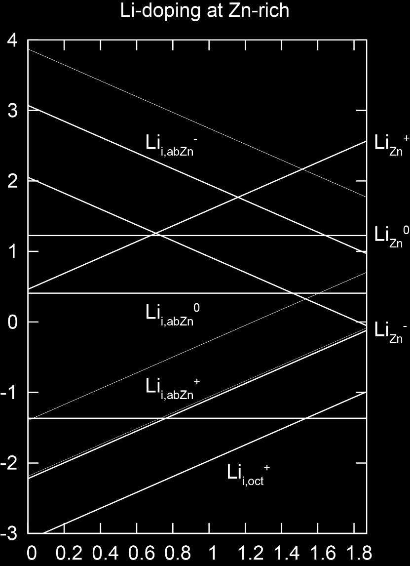

20 Preliminary results on Li dopant Formation energy (ev) Formation energy (ev) Fermi level (ev) Fermi level (ev)
 H(+/ ) level Formation Energy of MgO:H")
 H + stable")
 can be a reference level to align")
21 High-throughput ab initio screening III: band alignment of oxides Formation energy (ev) H(+/ ) level Formation Energy of MgO:H (GGA) H- H0 H+ H(+/ ) level VBM E F (ev) CBM C. G. Van de Walle et al, Nature 423, 626 (2003) H + stable configuration H - stable configuration - H(+/-) level as the charge neutrality level (CNL) can be a reference level to align relative band positions of solids.
22 Summary We are developing programs for automatic high-throughput ab initio computations With decent computational resources, it is possible to compute a certain bulk property with the speed of ~500 structures per month. We built a materials map related to band gap and dielectric constants and found several candidate high-k dielectrics that worth experimental investigation. We are expanding the automated ab initio screening to find suitable dopants in ZnO and band alignment of various oxides.
Computational discovery of p-type transparent oxide semiconductors using
 Computational discovery of p-type transparent oxide semiconductors using hydrogen descriptor Kanghoon Yim 1,*,, Yong Youn 1,*, Miso Lee 1, Dongsun Yoo 1, Joohee Lee 1, Sung Haeng Cho 2 & Seungwu Han 1
Supporting Information
 Electronic Supplementary Material (ESI) for Nanoscale. This journal is The Royal Society of Chemistry 2015 Supporting Information Single Layer Lead Iodide: Computational Exploration of Structural, Electronic
Theory of Hydrogen-Related Levels in Semiconductors and Oxides
 Theory of Hydrogen-Related Levels in Semiconductors and Oxides Chris G. Van de Walle Materials Department University of California, Santa Barbara Acknowledgments Computations J. Neugebauer (Max-Planck-Institut,
Semiconductors. SEM and EDAX images of an integrated circuit. SEM EDAX: Si EDAX: Al. Institut für Werkstoffe der ElektrotechnikIWE
 SEM and EDAX images of an integrated circuit SEM EDAX: Si EDAX: Al source: [Cal 99 / 605] M&D-.PPT, slide: 1, 12.02.02 Classification semiconductors electronic semiconductors mixed conductors ionic conductors
EECS143 Microfabrication Technology
 EECS143 Microfabrication Technology Professor Ali Javey Introduction to Materials Lecture 1 Evolution of Devices Yesterday s Transistor (1947) Today s Transistor (2006) Why Semiconductors? Conductors e.g
Defects in Semiconductors
 Defects in Semiconductors Mater. Res. Soc. Symp. Proc. Vol. 1370 2011 Materials Research Society DOI: 10.1557/opl.2011. 771 Electronic Structure of O-vacancy in High-k Dielectrics and Oxide Semiconductors
Defects and diffusion in metal oxides: Challenges for first-principles modelling
 Defects and diffusion in metal oxides: Challenges for first-principles modelling Karsten Albe, FG Materialmodellierung, TU Darmstadt Johan Pohl, Peter Agoston, Paul Erhart, Manuel Diehm FUNDING: ICTP Workshop
EE143 Fall 2016 Microfabrication Technologies. Evolution of Devices
 EE143 Fall 2016 Microfabrication Technologies Prof. Ming C. Wu wu@eecs.berkeley.edu 511 Sutardja Dai Hall (SDH) 1-1 Evolution of Devices Yesterday s Transistor (1947) Today s Transistor (2006) 1-2 1 Why
SCIENCE CHINA Physics, Mechanics & Astronomy. Electronic structure and optical properties of N-Zn co-doped -Ga 2 O 3
 SCIENCE CHINA Physics, Mechanics & Astronomy Article April 2012 Vol.55 No.4: 654 659 doi: 10.1007/s11433-012-4686-9 Electronic structure and optical properties of N-Zn co-doped -Ga 2 O 3 YAN JinLiang *
Real and virtual screening for materials discovery through first principles calculations
 Real and virtual screening for materials discovery through first principles calculations Isao Tanaka 1,2,3,4 1 Department of Materials Science and Engineering, Kyoto University, JAPAN 2 Elements Strategy
6. Computational Design of Energy-related Materials
 6. Computational Design of Energy-related Materials Contents 6.1 Atomistic Simulation Methods for Energy Materials 6.2 ab initio design of photovoltaic materials 6.3 Solid Ion Conductors for Fuel Cells
Electrochemistry. Part One: Introduction to Electrolysis and the Electrolysis of Molten Salts
 Part One: Introduction to Electrolysis and the Electrolysis of Molten Salts What do I need to know about electrochemistry? Electrochemistry Learning Outcomes: Candidates should be able to: a) Describe
Unique phenomena of tungsten associated with fusion reactor: uncertainties of stable hydrogen configuration tapped in tungsten vacancy
 Unique phenomena of tungsten associated with fusion reactor: uncertainties of stable hydrogen configuration tapped in tungsten vacancy Kyushu University Kazuhito Ohsawa Technical Meeting of the International
Classification of Solids
 Classification of Solids Classification by conductivity, which is related to the band structure: (Filled bands are shown dark; D(E) = Density of states) Class Electron Density Density of States D(E) Examples
A COMPUTATIONAL INVESTIGATION OF MIGRATION ENTHALPIES AND ELECTRONIC STRUCTURE IN SrFeO 3-δ
 A COMPUTATIONAL INVESTIGATION OF MIGRATION ENTHALPIES AND ELECTRONIC STRUCTURE IN SrFeO 3-δ A. Predith and G. Ceder Massachusetts Institute of Technology Department of Materials Science and Engineering
EECS130 Integrated Circuit Devices
 EECS130 Integrated Circuit Devices Professor Ali Javey 8/30/2007 Semiconductor Fundamentals Lecture 2 Read: Chapters 1 and 2 Last Lecture: Energy Band Diagram Conduction band E c E g Band gap E v Valence
ELEMENTARY BAND THEORY
 ELEMENTARY BAND THEORY PHYSICIST Solid state band Valence band, VB Conduction band, CB Fermi energy, E F Bloch orbital, delocalized n-doping p-doping Band gap, E g Direct band gap Indirect band gap Phonon
ECE 340 Lecture 39 : MOS Capacitor II
 ECE 340 Lecture 39 : MOS Capacitor II Class Outline: Effects of Real Surfaces Threshold Voltage MOS Capacitance-Voltage Analysis Things you should know when you leave Key Questions What are the effects
Earth Materials I Crystal Structures
 Earth Materials I Crystal Structures Isotopes same atomic number, different numbers of neutrons, different atomic mass. Ta ble 1-1. Su mmar y of quantu m num bers Name Symbol Values Principal n 1, 2,
3rd International Conference on Machinery, Materials and Information Technology Applications (ICMMITA 2015)
") 3rd International Conference on Machinery, Materials and Information Technology Applications (ICMMITA 2015) Study on Energy Band-gap Calculation of CuGaS 2 Liuyang YUa, Yong Xub, Kegao LIUc* School of
3rd International Conference on Machinery, Materials and Information Technology Applications (ICMMITA 2015) Study on Energy Band-gap Calculation of CuGaS 2 Liuyang YUa, Yong Xub, Kegao LIUc* School of
ᣂቇⴚ㗔 䇸䉮䊮䊏䊠䊷䊁䉞䉪䉴䈮䉋䉎 䊂䉱䉟䊮䋺ⶄว 㑐䈫㕖ᐔⴧ䉻䉟䊅䊚䉪䉴䇹 ᐔᚑ22ᐕᐲ ળ䇮2011ᐕ3 4ᣣ䇮 ੩ᄢቇᧄㇹ䉨䊞䊮䊌䉴 㗄 A02 ኒᐲ 㑐ᢙᴺℂ 䈮ၮ䈨䈒㕖ᐔⴧ 䊅䊉䉴䉬䊷䊦㔚 વዉ䉻䉟䊅䊚䉪䉴 ઍ ᄢᎿ ㆺ
 22201134 A02 GCOE Si device (further downsizing) Novel nanostructures (such as atomic chain) Nanoscale multi-terminal resistance measurement Carbon nanotube transistor Atomic switch Interplay:l Dynamics:
Transparent Electrode Applications
 Transparent Electrode Applications LCD Solar Cells Touch Screen Indium Tin Oxide (ITO) Zinc Oxide (ZnO) - High conductivity - High transparency - Resistant to environmental effects - Rare material (Indium)
Chapter 4: Bonding in Solids and Electronic Properties. Free electron theory
 Chapter 4: Bonding in Solids and Electronic Properties Free electron theory Consider free electrons in a metal an electron gas. regards a metal as a box in which electrons are free to move. assumes nuclei
Self-compensating incorporation of Mn in Ga 1 x Mn x As
 Self-compensating incorporation of Mn in Ga 1 x Mn x As arxiv:cond-mat/0201131v1 [cond-mat.mtrl-sci] 9 Jan 2002 J. Mašek and F. Máca Institute of Physics, Academy of Sciences of the CR CZ-182 21 Praha
First-principle Study for Al x Ga 1-x P and Mn-doped AlGaP 2 Electronic Properties
 Journal of Magnetics 20(4), 331-335 (2015) ISSN (Print) 1226-1750 ISSN (Online) 2233-6656 http://dx.doi.org/10.4283/jmag.2015.20.4.331 First-principle Study for Al x Ga 1-x P and Mn-doped AlGaP 2 Electronic
Chapter 3 (part 3) The Structures of Simple Solids
 The Structures of Simple Solids") CHM 511 chapter 3 page 1 of 9 Chapter 3 (part 3) The Structures of Simple Solids Rationalizing Structures Ionic radii As noted earlier, a reference value is needed. Usually oxygen is assumed to be 140
CHM 511 chapter 3 page 1 of 9 Chapter 3 (part 3) The Structures of Simple Solids Rationalizing Structures Ionic radii As noted earlier, a reference value is needed. Usually oxygen is assumed to be 140
Electrons, Holes, and Defect ionization
 Electrons, Holes, and Defect ionization The process of forming intrinsic electron-hole pairs is excitation a cross the band gap ( formation energy ). intrinsic electronic reaction : null e + h When electrons
Electrical material properties
 Electrical material properties U = I R Ohm s law R = ρ (l/a) ρ resistivity l length σ = 1/ρ σ conductivity A area σ = n q μ n conc. of charge carriers q their charge μ their mobility μ depends on T, defects,
Material Science II. d Electron systems
 Material Science II. d Electron systems 1. Electronic structure of transition-metal ions (May 23) 2. Crystal structure and band structure (June 13) 3. Mott s (June 20) 4. Metal- transition (June 27) 5.
(a) (b) Supplementary Figure 1. (a) (b) (a) Supplementary Figure 2. (a) (b) (c) (d) (e)
 (b) Supplementary Figure 1. (a) (b) (a) Supplementary Figure 2. (a) (b) (c) (d) (e)") (a) (b) Supplementary Figure 1. (a) An AFM image of the device after the formation of the contact electrodes and the top gate dielectric Al 2 O 3. (b) A line scan performed along the white dashed line
(a) (b) Supplementary Figure 1. (a) An AFM image of the device after the formation of the contact electrodes and the top gate dielectric Al 2 O 3. (b) A line scan performed along the white dashed line
Minimal Update of Solid State Physics
 Minimal Update of Solid State Physics It is expected that participants are acquainted with basics of solid state physics. Therefore here we will refresh only those aspects, which are absolutely necessary
ELECTRONIC AND STRUCTURAL PROPERTIES OF TIN DIOXIDE IN CUBIC PHASE *
 Iranian Journal of Science & Technology, Transaction A, Vol. 34, No. A Printed in the Islamic Republic of Iran, 1 Shiraz University ELECTRONIC AND STRUCTURAL PROPERTIES OF TIN DIOXIDE IN CUBIC PHASE *
Chapter 10: Modern Atomic Theory and the Periodic Table. How does atomic structure relate to the periodic table? 10.1 Electromagnetic Radiation
 Chapter 10: Modern Atomic Theory and the Periodic Table How does atomic structure relate to the periodic table? 10.1 Electromagnetic Radiation Electromagnetic (EM) radiation is a form of energy that exhibits
Lecture 2 Electrons and Holes in Semiconductors
 EE 471: Transport Phenomena in Solid State Devices Spring 2018 Lecture 2 Electrons and Holes in Semiconductors Bryan Ackland Department of Electrical and Computer Engineering Stevens Institute of Technology
EE130: Integrated Circuit Devices
 EE130: Integrated Circuit Devices (online at http://webcast.berkeley.edu) Instructor: Prof. Tsu-Jae King (tking@eecs.berkeley.edu) TA s: Marie Eyoum (meyoum@eecs.berkeley.edu) Alvaro Padilla (apadilla@eecs.berkeley.edu)
Outline. Introduction: graphene. Adsorption on graphene: - Chemisorption - Physisorption. Summary
 Outline Introduction: graphene Adsorption on graphene: - Chemisorption - Physisorption Summary 1 Electronic band structure: Electronic properties K Γ M v F = 10 6 ms -1 = c/300 massless Dirac particles!
Lecture 7: Extrinsic semiconductors - Fermi level
 Lecture 7: Extrinsic semiconductors - Fermi level Contents 1 Dopant materials 1 2 E F in extrinsic semiconductors 5 3 Temperature dependence of carrier concentration 6 3.1 Low temperature regime (T < T
1. Following Dalton s Atomic Theory, 2. In 1869 Russian chemist published a method. of organizing the elements. Mendeleev showed that
 20 CHEMISTRY 11 D. Organizing the Elements The Periodic Table 1. Following Dalton s Atomic Theory, By 1817, chemists had discovered 52 elements and by 1863 that number had risen to 62. 2. In 1869 Russian
Chapter 3: Elements and Compounds. 3.1 Elements
 Chapter 3: Elements and Compounds 3.1 Elements An element is a fundamental substance that cannot be broken down by chemical or physical methods to simpler substances. The 118 known elements are nature
Surfaces, Interfaces, and Layered Devices
 Surfaces, Interfaces, and Layered Devices Building blocks for nanodevices! W. Pauli: God made solids, but surfaces were the work of Devil. Surfaces and Interfaces 1 Interface between a crystal and vacuum
Supplementary Figure 2 Photoluminescence in 1L- (black line) and 7L-MoS 2 (red line) of the Figure 1B with illuminated wavelength of 543 nm.
 and 7L-MoS 2 (red line) of the Figure 1B with illuminated wavelength of 543 nm.") PL (normalized) Intensity (arb. u.) 1 1 8 7L-MoS 1L-MoS 6 4 37 38 39 4 41 4 Raman shift (cm -1 ) Supplementary Figure 1 Raman spectra of the Figure 1B at the 1L-MoS area (black line) and 7L-MoS area (red
PL (normalized) Intensity (arb. u.) 1 1 8 7L-MoS 1L-MoS 6 4 37 38 39 4 41 4 Raman shift (cm -1 ) Supplementary Figure 1 Raman spectra of the Figure 1B at the 1L-MoS area (black line) and 7L-MoS area (red
Organic Electronic Devices
 Organic Electronic Devices Week 5: Organic Light-Emitting Devices and Emerging Technologies Lecture 5.5: Course Review and Summary Bryan W. Boudouris Chemical Engineering Purdue University 1 Understanding
Lecture 1. OUTLINE Basic Semiconductor Physics. Reading: Chapter 2.1. Semiconductors Intrinsic (undoped) silicon Doping Carrier concentrations
 silicon Doping Carrier concentrations") Lecture 1 OUTLINE Basic Semiconductor Physics Semiconductors Intrinsic (undoped) silicon Doping Carrier concentrations Reading: Chapter 2.1 EE105 Fall 2007 Lecture 1, Slide 1 What is a Semiconductor? Low
Lecture 1 OUTLINE Basic Semiconductor Physics Semiconductors Intrinsic (undoped) silicon Doping Carrier concentrations Reading: Chapter 2.1 EE105 Fall 2007 Lecture 1, Slide 1 What is a Semiconductor? Low
Bonding in Solids. What is the chemical bonding? Bond types: Ionic (NaCl vs. TiC?) Covalent Van der Waals Metallic
 Covalent Van der Waals Metallic") Bonding in Solids What is the chemical bonding? Bond types: Ionic (NaCl vs. TiC?) Covalent Van der Waals Metallic 1 Ions and Ionic Radii LiCl 2 Ions (a) Ions are essentially spherical. (b) Ions may be
Bonding in Solids What is the chemical bonding? Bond types: Ionic (NaCl vs. TiC?) Covalent Van der Waals Metallic 1 Ions and Ionic Radii LiCl 2 Ions (a) Ions are essentially spherical. (b) Ions may be
Supporting Information. First-Principles Study: Tuning the Redox Behavior of Li-Rich
 Supporting Information First-Principles Study: Tuning the Redox Behavior of Li-Rich Layered Oxides by Chlorine Doping Huijun Yan 1, Biao Li 1, Zhen Yu 2, Wangsheng Chu 2, Dingguo Xia 1* 1 Beijing Key Laboratory
Supplementary Information
 Supplementary Information Supplementary Figure 1: After structural optimization of the CH 3 NH 3 PbI 3 unit cell, the resulting relaxed volumes for three distinct orientation of the MA molecules are shown.
Graphene and Carbon Nanotubes
 Graphene and Carbon Nanotubes 1 atom thick films of graphite atomic chicken wire Novoselov et al - Science 306, 666 (004) 100μm Geim s group at Manchester Novoselov et al - Nature 438, 197 (005) Kim-Stormer
SnO 2 Physical and Chemical Properties due to the Impurity Doping
 , March 13-15, 2013, Hong Kong SnO 2 Physical and Chemical Properties due to the Impurity Doping Richard Rivera, Freddy Marcillo, Washington Chamba, Patricio Puchaicela, Arvids Stashans Abstract First-principles
Potentials, periodicity
 Potentials, periodicity Lecture 2 1/23/18 1 Survey responses 2 Topic requests DFT (10), Molecular dynamics (7), Monte Carlo (5) Machine Learning (4), High-throughput, Databases (4) NEB, phonons, Non-equilibrium
Forming Chemical Bonds
 Forming Chemical Bonds Chemical Bonds Three basic types of bonds 2012 Pearson Education, Inc. Ionic Electrostatic attraction between ions. Covalent Sharing of electrons. Metallic Metal atoms bonded to
Improving the solar cells efficiency of metal Sulfide thin-film nanostructure via first principle calculations
 Improving the solar cells efficiency of metal Sulfide thin-film nanostructure via first principle calculations Alwaleed Adllan Abusin, PhD Elzina Bala Africa City of Technology Agenda INTRODUCTION TO HIGH-PERFORMANCE
Supplementary Information
 Supplementary Information Supplementary Figure 1: Electronic Kohn-Sham potential profile of a charged monolayer MoTe 2 calculated using PBE-DFT. Plotted is the averaged electronic Kohn- Sham potential
Introduction to Engineering Materials ENGR2000. Dr.Coates
 Introduction to Engineering Materials ENGR2000 Chapter 18: Electrical Properties Dr.Coates 18.2 Ohm s Law V = IR where R is the resistance of the material, V is the voltage and I is the current. l R A
materials and their properties
 materials and their properties macroscopic properties phase state strength / stiffness electrical conductivity chemical properties color / transparence spectroscopical properties surface properties density
single-layer transition metal dichalcogenides MC2
 single-layer transition metal dichalcogenides MC2 Period 1 1 H 18 He 2 Group 1 2 Li Be Group 13 14 15 16 17 18 B C N O F Ne 3 4 Na K Mg Ca Group 3 4 5 6 7 8 9 10 11 12 Sc Ti V Cr Mn Fe Co Ni Cu Zn Al Ga
NUMERICAL CALCULATION OF THE ELECTRON MOBILITY IN GaAs SEMICONDUCTOR UNDER WEAK ELECTRIC FIELD APPLICATION
 International Journal of Science, Environment and Technology, Vol. 1, No 2, 80-87, 2012 NUMERICAL CALCULATION OF THE ELECTRON MOBILITY IN GaAs SEMICONDUCTOR UNDER WEAK ELECTRIC FIELD APPLICATION H. Arabshahi,
All chemical bonding is based on the following relationships of electrostatics: 2. Each period on the periodic table
 UNIT VIII ATOMS AND THE PERIODIC TABLE 25 E. Chemical Bonding 1. An ELECTROSTATIC FORCE is All chemical bonding is based on the following relationships of electrostatics: The greater the distance between
Section 12: Intro to Devices
 Section 12: Intro to Devices Extensive reading materials on reserve, including Robert F. Pierret, Semiconductor Device Fundamentals Bond Model of Electrons and Holes Si Si Si Si Si Si Si Si Si Silicon
LN 3 IDLE MIND SOLUTIONS
 IDLE MIND SOLUTIONS 1. Let us first look in most general terms at the optical properties of solids with band gaps (E g ) of less than 4 ev, semiconductors by definition. The band gap energy (E g ) can
Chemical Bonding polarity & Dipole Moments. Chapter 8 Part III
 Chemical Bonding polarity & Dipole Moments Chapter 8 Part III Exercise Arrange the following bonds from most to least polar: a) N F O F C F b) C F N O Si F c) Cl Cl B Cl S Cl Exercise a) C F, N F, O F
Hardness Prediction and First Principle Study of Re-123(Re = Y, Eu, Pr, Gd) Superconductors
 Superconductors") 316 Bull. Korean Chem. Soc. 29, Vol. 3, No. 12 Weiwei Liu et al. DOI 1.512/bkcs.29.3.12.316 Hardness Prediction and First Principle Study of Re-123(Re = Y, Eu, Pr, Gd Superconductors Weiwei Liu,, Y. P.
316 Bull. Korean Chem. Soc. 29, Vol. 3, No. 12 Weiwei Liu et al. DOI 1.512/bkcs.29.3.12.316 Hardness Prediction and First Principle Study of Re-123(Re = Y, Eu, Pr, Gd Superconductors Weiwei Liu,, Y. P.
CHAPTER 6. ELECTRONIC AND MAGNETIC STRUCTURE OF ZINC-BLENDE TYPE CaX (X = P, As and Sb) COMPOUNDS
 COMPOUNDS") 143 CHAPTER 6 ELECTRONIC AND MAGNETIC STRUCTURE OF ZINC-BLENDE TYPE CaX (X = P, As and Sb) COMPOUNDS 6.1 INTRODUCTION Almost the complete search for possible magnetic materials has been performed utilizing
143 CHAPTER 6 ELECTRONIC AND MAGNETIC STRUCTURE OF ZINC-BLENDE TYPE CaX (X = P, As and Sb) COMPOUNDS 6.1 INTRODUCTION Almost the complete search for possible magnetic materials has been performed utilizing
M11/4/CHEMI/SPM/ENG/TZ2/XX CHEMISTRY STANDARD LEVEL PAPER 1. Monday 9 May 2011 (afternoon) 45 minutes INSTRUCTIONS TO CANDIDATES
 45 minutes INSTRUCTIONS TO CANDIDATES") M11/4/CHEMI/SPM/ENG/TZ/XX 116116 CHEMISTRY STANDARD LEVEL PAPER 1 Monday 9 May 011 (afternoon) 45 minutes INSTRUCTIONS TO CANDIDATES Do not open this examination paper until instructed to do so. Answer
M11/4/CHEMI/SPM/ENG/TZ/XX 116116 CHEMISTRY STANDARD LEVEL PAPER 1 Monday 9 May 011 (afternoon) 45 minutes INSTRUCTIONS TO CANDIDATES Do not open this examination paper until instructed to do so. Answer
Ch. 9 NOTES ~ Chemical Bonding NOTE: Vocabulary terms are in boldface and underlined. Supporting details are in italics.
 Ch. 9 NOTES ~ Chemical Bonding NOTE: Vocabulary terms are in boldface and underlined. Supporting details are in italics. I. Review: Comparison of ionic and molecular compounds Molecular compounds Ionic
Solid Surfaces, Interfaces and Thin Films
 Hans Lüth Solid Surfaces, Interfaces and Thin Films Fifth Edition With 427 Figures.2e Springer Contents 1 Surface and Interface Physics: Its Definition and Importance... 1 Panel I: Ultrahigh Vacuum (UHV)
Electrostatics of Nanowire Transistors
 Electrostatics of Nanowire Transistors Jing Guo, Jing Wang, Eric Polizzi, Supriyo Datta and Mark Lundstrom School of Electrical and Computer Engineering Purdue University, West Lafayette, IN, 47907 ABSTRACTS
Ø Draw the Bohr Diagrams for the following atoms: Sodium Potassium Rubidium
 Chemistry 11 Atomic Theory V Name: Date: Block: 1. Atomic Radius 2. Ionization Energy 3. Electronegativity 4. Chemical Bonding Atomic Radius Periodic Trends Ø As we move across a period or down a chemical
Inorganic Chemistry with Doc M. Day 9. Acids and Bases Overview
 Inorganic Chemistry with Doc M. Day 9. Acids and Bases Overview Topics: 1. Bronsted-Lowry Concept 5. ph of salts 2. Lewis acid and base concepts 6. Hard-soft acid and base theory 3. Oxyacids 7. Non-aqueous
Name Date Class STUDY GUIDE FOR CONTENT MASTERY. covalent bond molecule sigma bond exothermic pi bond
 Covalent Bonding Section 9.1 The Covalent Bond In your textbook, read about the nature of covalent bonds. Use each of the terms below just once to complete the passage. covalent bond molecule sigma bond
Materials and Devices in Electrical Engineering
 Examination WS 02/03 Materials and Devices in Electrical Engineering Monday 17 th of March, 9:00 11:00, International Department, SR. 203 Notice 1. It is allowed to use any kind of aids (books, scripts,
Chapter 1 Overview of Semiconductor Materials and Physics
 Chapter 1 Overview of Semiconductor Materials and Physics Professor Paul K. Chu Conductivity / Resistivity of Insulators, Semiconductors, and Conductors Semiconductor Elements Period II III IV V VI 2 B
MME 467: Ceramics for Advanced Applications
 MME 467: Ceramics for Advanced Applications Lecture 26 Dielectric Properties of Ceramic Materials 2 1. Barsoum, Fundamental Ceramics, McGraw-Hill, 2000, pp.513 543 2. Richerson, Modern Ceramic Engineering,
Occurs when electrons are transferred electrostatic attractions (btw positive & negative atoms)
") Ionic Bonding Ionic Bonding Occurs when electrons are transferred from one atom to another, forming two ions The ions stay together because of electrostatic attractions (btw positive & negative atoms)
Ionic Bonding Ionic Bonding Occurs when electrons are transferred from one atom to another, forming two ions The ions stay together because of electrostatic attractions (btw positive & negative atoms)
and strong interlayer quantum confinement
 Supporting Information GeP3: A small indirect band gap 2D crystal with high carrier mobility and strong interlayer quantum confinement Yu Jing 1,3, Yandong Ma 1, Yafei Li 2, *, Thomas Heine 1,3 * 1 Wilhelm-Ostwald-Institute
First-principles studies of the structural, electronic, and optical properties of a novel thorium compound Rb 2 Th 7 Se 15
 First-principles studies of the structural, electronic, and optical properties of a novel thorium compound Rb 2 Th 7 Se 15 M.G. Brik 1 Institute of Physics, University of Tartu, Riia 142, Tartu 5114, Estonia
Defects in materials. Manish Jain. July 8, Department of Physics Indian Institute of Science Bangalore 1/46
 1/46 Defects in materials Manish Jain Department of Physics Indian Institute of Science Bangalore July 8, 2014 Outline 2/46 Motivation. Computational methods. Defects in oxides. Why are defects challenging?
4.1 Atomic structure and the periodic table. GCSE Chemistry
 4.1 Atomic structure and the periodic table GCSE Chemistry All substances are made of atoms this is cannot be chemically broken down it is the smallest part of an element. Elements are made of only one
Atomic Structure & Interatomic Bonding
 Atomic Structure & Interatomic Bonding Chapter Outline Review of Atomic Structure Atomic Bonding Atomic Structure Atoms are the smallest structural units of all solids, liquids & gases. Atom: The smallest
Energy storage: high performance material engineering
 Energy storage: high performance material engineering Teranishi Group Faculty of Engineering Research activities 1) Polarization assisted ultrahigh rate lithium ion batteries 1) Lithium ion conductor-dielectrics
Introduction into defect studies. in ceramic materials(iii) Structure, Defects and Defect Chemistry. Z. Wang. January 18, 2002
 Structure, Defects and Defect Chemistry. Z. Wang. January 18, 2002") Introduction into defect studies in ceramic materials(iii) Structure, Defects and Defect Chemistry Z. Wang January 18, 2002 1. Mass, Charge and Site Balance The Schottky reactions for NaCl and MgO, respectively,
Introduction into defect studies in ceramic materials(iii) Structure, Defects and Defect Chemistry Z. Wang January 18, 2002 1. Mass, Charge and Site Balance The Schottky reactions for NaCl and MgO, respectively,
PART CHAPTER2. Atomic Bonding
 PART O N E APTER2 Atomic Bonding The scanning tunneling microscope (Section 4.7) allows the imaging of individual atoms bonded to a material surface. In this case, the microscope was also used to manipulate
Ab initio Berechungen für Datenbanken
 J Ab initio Berechungen für Datenbanken Jörg Neugebauer University of Paderborn Lehrstuhl Computational Materials Science Computational Materials Science Group CMS Group Scaling Problem in Modeling length
Defects in TiO 2 Crystals
 , March 13-15, 2013, Hong Kong Defects in TiO 2 Crystals Richard Rivera, Arvids Stashans 1 Abstract-TiO 2 crystals, anatase and rutile, have been studied using Density Functional Theory (DFT) and the Generalized
Pseudopotentials: design, testing, typical errors
 Pseudopotentials: design, testing, typical errors Kevin F. Garrity Part 3 National Institute of Standards and Technology (NIST) Uncertainty Quantification in Materials Modeling 2015 Testing Basis Sets
ET3034TUx Utilization of band gap energy
 ET3034TUx - 3.3.1 - Utilization of band gap energy In the last two weeks we have discussed the working principle of a solar cell and the external parameters that define the performance of a solar cell.
Relation Between Refractive Index, Micro Hardness and Bulk Modulus of A II B VI and A III B V Semiconductors
 International Journal of Pure and Applied Physics ISSN 0973-1776 Volume 5, Number 3 (2009), pp. 271-276 Research India Publications http://www.ripublication.com/ijpap.htm Relation Between Refractive Index,
Title of file for HTML: Supplementary Information Description: Supplementary Figures, Supplementary Tables and Supplementary References
 Title of file for HTML: Supplementary Information Description: Supplementary Figures, Supplementary Tables and Supplementary References Title of file for HTML: Supplementary Movie 1 Description: This movie
CH676 Physical Chemistry: Principles and Applications. CH676 Physical Chemistry: Principles and Applications
 CH676 Physical Chemistry: Principles and Applications Band Theory Fermi-Dirac Function f(e) = 1/[1 + e (E-E F)/kT ] Where the Fermi Energy, E F, is defined as the energy where f(e) = 1/2. That is to say
Journal of Atoms and Molecules
 Research article Journal of Atoms and Molecules An International Online Journal ISSN 77 147 Hot Electron Transport in Polar Semiconductor at Low Lattice Temperature A. K. Ghorai Physics Department, Kalimpong
Electrical Properties
 Electrical Properties Electrical Conduction R Ohm s law V = IR I l Area, A V where I is current (Ampere), V is voltage (Volts) and R is the resistance (Ohms or ) of the conductor Resistivity Resistivity,
Department of Electrical Engineering and Information Systems, Tanaka-Ohya lab.
 Observation of the room-temperature local ferromagnetism and its nanoscale expansion in the ferromagnetic semiconductor Ge 1 xfe x Yuki K. Wakabayashi 1 and Yukio Takahashi 2 1 Department of Electrical
Status of the AMoRE experiment searching for neutrinoless double beta decay of 100 Mo
 Status of the AMoRE experiment searching for neutrinoless double beta decay of 100 Mo Hyon-Suk Jo Center for Underground Physics Institute for Basic Science INPC 2016 - Adelaide Convention Centre, Australia
Ch. 2: Energy Bands And Charge Carriers In Semiconductors
 Ch. 2: Energy Bands And Charge Carriers In Semiconductors Discrete energy levels arise from balance of attraction force between electrons and nucleus and repulsion force between electrons each electron
I-V characteristics model for Carbon Nanotube Field Effect Transistors
 International Journal of Engineering & Technology IJET-IJENS Vol:14 No:04 33 I-V characteristics model for Carbon Nanotube Field Effect Transistors Rebiha Marki, Chérifa Azizi and Mourad Zaabat. Abstract--
MOS CAPACITOR AND MOSFET
 EE336 Semiconductor Devices 1 MOS CAPACITOR AND MOSFET Dr. Mohammed M. Farag Ideal MOS Capacitor Semiconductor Devices Physics and Technology Chapter 5 EE336 Semiconductor Devices 2 MOS Capacitor Structure
100% ionic compounds do not exist but predominantly ionic compounds are formed when metals combine with non-metals.
 2.21 Ionic Bonding 100% ionic compounds do not exist but predominantly ionic compounds are formed when metals combine with non-metals. Forming ions Metal atoms lose electrons to form +ve ions. Non-metal
per unit cell Motif: Re at (0, 0, 0); 3O at ( 1 / 2, 0), (0, 0, 1 / 2 ) Re: 6 (octahedral coordination) O: 2 (linear coordination) ReO 6
; 3O at ( 1 / 2, 0), (0, 0, 1 / 2 ) Re: 6 (octahedral coordination) O: 2 (linear coordination) ReO 6") Lattice: Primitive Cubic 1ReO 3 per unit cell Motif: Re at (0, 0, 0); 3O at ( 1 / 2, 0, 0), (0, 1 / 2, 0), (0, 0, 1 / 2 ) Re: 6 (octahedral coordination) O: 2 (linear coordination) ReO 6 octahedra share
Lattice: Primitive Cubic 1ReO 3 per unit cell Motif: Re at (0, 0, 0); 3O at ( 1 / 2, 0, 0), (0, 1 / 2, 0), (0, 0, 1 / 2 ) Re: 6 (octahedral coordination) O: 2 (linear coordination) ReO 6 octahedra share
INTRODUCTION TO THE DEFECT STATE IN MATERIALS
 INTRODUCTION TO THE DEFECT STATE IN MATERIALS DEFECTS, DEFECTS, DEFECTS CAN T LIVE WITH THEM!!! CAN T LIVE WITHOUT THEM!!! INTRODUCTION TO DEFECT STATE IN MATERIALS DEFECTS, DEFECTS, DEFECTS Perfect crystals
EPSC 233. Compositional variation in minerals. Recommended reading: PERKINS, p. 286, 41 (Box 2-4).
.") EPSC 233 Compositional variation in minerals Recommended reading: PERKINS, p. 286, 41 (Box 2-4). Some minerals are nearly pure elements. These are grouped under the category of native elements. This includes
EPSC 233 Compositional variation in minerals Recommended reading: PERKINS, p. 286, 41 (Box 2-4). Some minerals are nearly pure elements. These are grouped under the category of native elements. This includes
Lecture 3b. Bonding Model and Dopants. Reading: (Cont d) Notes and Anderson 2 sections
 Notes and Anderson 2 sections") Lecture 3b Bonding Model and Dopants Reading: (Cont d) Notes and Anderson 2 sections 2.3-2.7 The need for more control over carrier concentration Without help the total number of carriers (electrons and
Lecture 3b Bonding Model and Dopants Reading: (Cont d) Notes and Anderson 2 sections 2.3-2.7 The need for more control over carrier concentration Without help the total number of carriers (electrons and