Defects and diffusion in metal oxides: Challenges for first-principles modelling
|
|
|
- Lucas Gibbs
- 5 years ago
- Views:
Transcription


1 Defects and diffusion in metal oxides: Challenges for first-principles modelling Karsten Albe, FG Materialmodellierung, TU Darmstadt Johan Pohl, Peter Agoston, Paul Erhart, Manuel Diehm FUNDING: ICTP Workshop DFG-SFB , BMBF Gracis, Helmholtz Virtual Institute MiCo, Schott Solar
2 How To Get Hydrogen? Renewable Energy Heat Biomass Mechanical Energy Thermolysis Electricity Electrolysis Conversion Photolysis No CO 2 emission 20% theo. efficiency Hydrogen


3 Photocatalysis: Desired Materials Properties 1.23 ev < band gap 3eV Engineered pathways of electron-hole pairs No defects acting as recombination sites Charge transfer used for water splitting instead of corrosion Efficient H 2 production and low overvoltages h Identify transparent passivating surface layer Couple Fermi level of metal catalyst to the quasi-fermi levels of the semiconductor under illumination Design a working device Design and implement assembling procedures n-region p-region


4 Materials by Design Design Concept Device Integration Tailored Band Gaps Tailored Surfaces and Interfaces Tailored Nanostructures
5 Materials by Design Design Concept Tailored Band Gaps
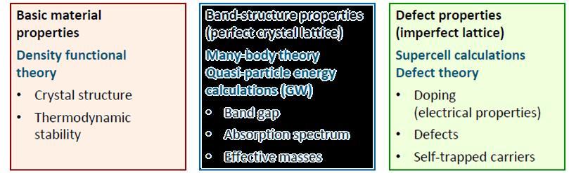

6 Electronic Structure Theory
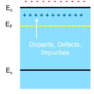
7 Defects in Semiconductors
8 Ab-initio Thermodynamics of Point Defects Determination of the ground-state properties of pure phases Ground-states of defects in super cells Calculation of the formation energies at the VBM Correction of size effects Determination of the defect formation enthalpies as a function of the fermi energy and the chemical potentials in equilibrium Self-consistent determination of the fermi level
9 When DFT fails In defect calculations: band gaps Heavily underestimated Both LDA/GGA functionals Affects: Defect levels Defect formation energies Correction: scissor operation! Shift the conduction band Align E g (DFT) and E g (EXP) Donor type defects follow CB Correct formation energies Alternative: hybrid or semi-empirical functionals


10 Pt/CuGaSe2 and Pt/CdS/CuGaSe2 as Photoelectrode 0.1 M Na 2 SO 4 aq. (ph 9), 300 W Xe lamp, 5 mv s- 1

11 Band gap in ev Chalcopyrite Band Gaps from HSE06 Electronic band gaps (ev) with optimized exchange screening parameter = 0.13: 3,00 2,50 2,00 1,50 1,00 GGA HSE06 Experiment Chalcopyrite 0,50 0,00 CuInSe 2 CuGaSe 2 CuInS 2 CuGaS 2 CuIn 5 Se 8 J. Pohl, K. Albe, J. Appl. Phys. 108, (2010)
12 Defects in CuInSe 2 Phase stability Point defect formation enthalpies J. Pohl, K. Albe, Phys. Rev. B 87, (2013)
13 Defects in CuInSe 2 Phase stability Point defect formation enthalpies J. Pohl, K. Albe, Phys. Rev. B 87, (2013)
14 Defects in CuInSe 2 Phase stability Point defect formation enthalpies J. Pohl, K. Albe, Phys. Rev. B 87, (2013)

15 Defects in CuGaSe 2 Phase stability Point defect formation enthalpies J. Pohl, K. Albe, Phys. Rev. B 87, (2013)
16 Antisite Defects in CuInSe 2 and CuGaSe 2 Conduction band edge 1.68 ev 1.04 ev Ga Cu 1.33 ev (+1/0) 1.26 ev (+2/+1) 0.67 ev 0.74 ev (-1/-2) Cu In,Ga 0.11 ev 0.21 ev (0/-1) 0.0 CuInSe 2 Valence band edge CuGaSe 2
17 Conclusions on CIGS For a typical Cu(In,Ga)Se 2 absorber with [Ga]/[Ga]+[In]=0.25, Cu In and Cu Ga hole traps are the most detrimental defects! Copper-rich conditions maximize the concentration of this defect. For [Ga]/[Ga]+[In] > 0.5, Ga Cu becomes a deep minority carrier trap and can limit device efficiency. Optimal conditions to minimize Cu In and Cu Ga are located on the copper-poor side, with not too high Se/metal-ratio!
![SnO 2 : Intrinsic Conductivity and p(o 2 ) 1 2 K O V 2e O O 2 ( T) O 1 P [ V ][ e ]](/docs-images/94/120362989/images/18-2.jpg "1/2 2 O O 2 O Is standard defect chemistry correct?")
18 SnO 2 : Intrinsic Conductivity and p(o 2 ) 1 2 K O V 2e O O 2 ( T) O 1 P [ V ][ e ] 1/2 2 O O 2 O Is standard defect chemistry correct? Whats about other intrinsic defects?


19 TCO: What do we expect? deep - Donor Intrinsic n-typetco shallow - Donor In principle oxygen vacancies or cation interstitals can be donors

 245501, Phys. Rev. Lett. 106 (2011) 069602")
20 O-Vacancy Constant formation energies for the neutral charge state Strongly reduced formation energies for positive charge states Indium oxide and tin oxide are truly intrinsically n-type semiconductors The behavior is more complex for ZnO Agoston, Albe/ Phys. Rev. Lett. 103 (2009) , Phys. Rev. Lett. 106 (2011)
 245501, Phys. Rev. Lett.")
21 Band Gaps and Defect States Phys. Rev. Lett. 103 (2009) , Phys. Rev. Lett. 106 (2011)
22 Acceptor Defects Increased formation energies of acceptor defects in all TCOs Doping limits agree with experiment for In 2 O 3 but not for SnO 2

23 SnO 2 vs. In 2 O 3 Doped SnO 2 has no oxygen interstitials! Therefore high conductivities can be expected P. Agoston, C. Körber, A. Klein, M. J. Puska, R. M. Nieminen and K. Albe, J. Appl. Phys C. Körber P. Ágoston, A. Klein Sensors and Actuators B (2009)
24 Diffusion: Migration Barriers D f m f O (, 2 m S S H E f p ) H ( E f) 2 0 f exp exp k kt D 0 G TST 0 G 0 G m

25 Point defects in ZnO: Kinetics Appl. Phys. Lett. 88, (2006)
26 Materials by Design Design Concept Tailored Band Gaps Tailored Surfaces and Interfaces

 : 2 3 5 Experiment")

27 ITO-(001) Oxygen : Indium : Oxygen (1. layer) : Indium (1. layer) : Experiment Experiment E. Morales, U. Diebold, Appl. Phys. Lett., 139, (2009)
28 In 2 O 3 -(001) Oxygen : Indium : Oxygen (1. layer) : Indium (1. layer) : Simulation Simulation Simulation Experiment Experiment 2 3 5

 : 2 3 5")


29 In 2 O 3 -(001) Oxygen : Indium : Oxygen (1. layer) : Indium (1. layer) : Simulation Simulation Simulation Experiment No compelling agreement with experiment Experiment 2 3 5


30 Doping Effect Peroxide splitting highly favorable
31 ITO-(001) Oxygen : Indium : Oxygen (1. layer) : Indium (1. layer) : Simulation Experiment P. Agoston, K. Albe, Phys. Rev. B 84, (2011)


32 ITO-(001) Oxygen : Indium : Oxygen (1. layer) : Indium (1. layer) : Improved agreement with experiment when the effect of doping is considered
33 Thermodynamics of Nanomaterials
34 Materials by Design Design Concept Tailored Band Gaps Tailored Surfaces and Interfaces Tailored Nanostructures


35 Volume Strain by Surface Stresses MgO (compressive): GaN (tensile)
36 Surface Energy vs. Surface Stress Surface Energy Surface Stress f ij Work required to produce extra surface Work required to enlarge/minimize existing surface dw da dw d A f Ad ij ij f f ij 1 A d A d d d ij
37 Calculated Surface Stresses (DFT)
38 Lattice Expansion
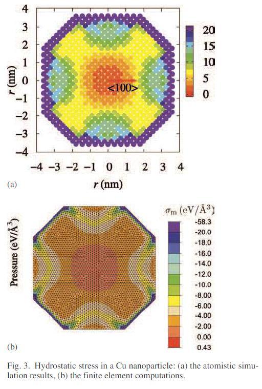
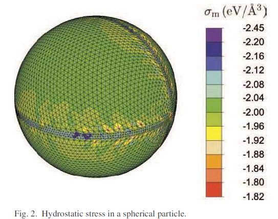
39 Stress Distribution: MD vs. FEM
40 Ab-initio Phase Diagrams Calculate the total energies of a set of structures (e.g. from DFT) Fit a model Hamiltonian to the set of structures (least squares fit / genetic algorithm) Predict new ground states or just include more structures Calculate the phase diagram (using Monte Carlo)
41 BOS-Model How to calculate the energy of a binary alloy system with two species A and B? Refined Bond Order Simulation Mixing model (BOS: Zhu, depristo 1995) where is the site energy of an atom of species A with coordination Z is the number of odd neighbors in the n-th shell is the difference in the site energy when changing a n-th neighbor to odd species is an asymmetry parameter (asymmetry considered for nearest neighbors only) (for species B replace and ) (Pohl, Albe, Acta Materialia 57, 4140 (2009))
42 Bulk Phase Diagram Pt-Rh Theoretical Pt-Rh Bulk phase diagram Gibb s Free Energy surface Warren-Cowley Short Range Order Parameters (Pohl, Albe, ACTA MAT 57, 4140 (2009))
43 Nanophase diagram Effects for shrinking particle size: ordering temperature sinks concentration stability range of some ordered phases broadens stable phases shift towards higher concentrations of segregating species (Pt) two-phase regions shrink Beilstein J. Nanotechnol. 2012, 3, 1 11.
44 2 % Pt, Diameter 7.8 nm

45 6 % Pt
46 10 % Pt
47 18% Pt
48 28 % Pt
49 28% Pt
50 42% Pt
51 44% Pt
52 46% Pt
53 46% Pt
54 60% Pt
55 60% Pt
56 86% Pt
57 86% Pt
58 Size-dependent Diffusion? Vacancy Mechanism D D 0 exp E k mig B T C V

59 Vacancies in Lattice Model: KMC Müller/Albe Acta Mat. (2007)
60 Vacancies in Lattice Model: KMC f E v 1.28 ev Model: Cu
61 Vacancy Formation Energy: Lattice model
62 Vacancies in Lattice Model f f 2 Ev( R) Ev( R ) R Surface energy Surface stress 2 /R f E v
63 Vacancies in Nanoparticles E ( R) E ( R ) f v f v 2 f V R Surface energy Surface stress f 2 /R f E v 2f / R V f E v : atomic volume V = : - Vrel:= formation volume

64 Surface Energy vs. Surface Stress Surface Energy Surface Stress f ij Work required to produce extra surface Work required to enlarge/minimize existing surface dw da dw d A f Ad ij ij f f ij 1 A d A d d d ij
65 Materials by Design Design Concept Device Integration Tailored Band Gaps Tailored Surfaces and Interfaces Tailored Nanostructures
66 Take home messages The properties of point defects and surfaces in oxides are most sensitive to the Fermi-energy We need Fermi-level engineering Defects not only go along with excess energies but also stresses Strain effects due to point, line and planar defects can be significant Thermodynamics and kinetics on the nanoscale can be very different We need a better understanding of nanoeffects
6. Computational Design of Energy-related Materials
 6. Computational Design of Energy-related Materials Contents 6.1 Atomistic Simulation Methods for Energy Materials 6.2 ab initio design of photovoltaic materials 6.3 Solid Ion Conductors for Fuel Cells
This is an electronic reprint of the original article. This reprint may differ from the original in pagination and typographic detail.
 Powered by TCPDF (www.tcpdf.org) This is an electronic reprint of the original article. This reprint may differ from the original in pagination and typographic detail. Ágoston, Péter; Albe, Karsten; Nieminen,
ESE 372 / Spring 2013 / Lecture 5 Metal Oxide Semiconductor Field Effect Transistor
 Metal Oxide Semiconductor Field Effect Transistor V G V G 1 Metal Oxide Semiconductor Field Effect Transistor We will need to understand how this current flows through Si What is electric current? 2 Back
Vacancies in CuInSe(2): new insights from hybrid-functional calculations
: new insights from hybrid-functional calculations") Zurich Open Repository and Archive University of Zurich Main Library Strickhofstrasse 39 CH-8057 Zurich www.zora.uzh.ch Year: 2011 Vacancies in CuInSe(2): new insights from hybrid-functional calculations
Zurich Open Repository and Archive University of Zurich Main Library Strickhofstrasse 39 CH-8057 Zurich www.zora.uzh.ch Year: 2011 Vacancies in CuInSe(2): new insights from hybrid-functional calculations
EFFECTS OF STOICHIOMETRY ON POINT DEFECTS AND IMPURITIES IN GALLIUM NITRIDE
 EFFECTS OF STOICHIOMETRY ON POINT DEFECTS AND IMPURITIES IN GALLIUM NITRIDE C. G. VAN DE WALLE AND J. E. NORTHRUP Palo Alto Research Center, 3333 Coyote Hill Road, Palo Alto, CA 930, USA E-mail: vandewalle@parc.com
Conduction-Band-Offset Rule Governing J-V Distortion in CdS/CI(G)S Solar Cells
S Solar Cells") Conduction-Band-Offset Rule Governing J-V Distortion in CdS/CI(G)S Solar Cells A. Kanevce, M. Gloeckler, A.O. Pudov, and J.R. Sites Physics Department, Colorado State University, Fort Collins, CO 80523,
Conduction-Band-Offset Rule Governing J-V Distortion in CdS/CI(G)S Solar Cells A. Kanevce, M. Gloeckler, A.O. Pudov, and J.R. Sites Physics Department, Colorado State University, Fort Collins, CO 80523,
PH575 Spring Lecture #19 Semiconductors: electrical & optical properties: Kittel Ch. 8 pp ; Ch. 20
 PH575 Spring 2014 Lecture #19 Semiconductors: electrical & optical properties: Kittel Ch. 8 pp. 205-214; Ch. 20 Simplified diagram of the filling of electronic band structure in various types of material,
Lecture 7: Extrinsic semiconductors - Fermi level
 Lecture 7: Extrinsic semiconductors - Fermi level Contents 1 Dopant materials 1 2 E F in extrinsic semiconductors 5 3 Temperature dependence of carrier concentration 6 3.1 Low temperature regime (T < T
Theory of Hydrogen-Related Levels in Semiconductors and Oxides
 Theory of Hydrogen-Related Levels in Semiconductors and Oxides Chris G. Van de Walle Materials Department University of California, Santa Barbara Acknowledgments Computations J. Neugebauer (Max-Planck-Institut,
Available online at Energy Procedia 00 (2009) Energy Procedia 2 (2010) E-MRS Spring meeting 2009, Symposium B
 Energy Procedia 2 (2010) E-MRS Spring meeting 2009, Symposium B") Available online at www.sciencedirect.com Energy Procedia 00 (2009) 000 000 Energy Procedia 2 (2010) 169 176 Energy Procedia www.elsevier.com/locate/procedia www.elsevier.com/locate/procedia E-MRS Spring
Available online at www.sciencedirect.com Energy Procedia 00 (2009) 000 000 Energy Procedia 2 (2010) 169 176 Energy Procedia www.elsevier.com/locate/procedia www.elsevier.com/locate/procedia E-MRS Spring
Chemistry Instrumental Analysis Lecture 8. Chem 4631
 Chemistry 4631 Instrumental Analysis Lecture 8 UV to IR Components of Optical Basic components of spectroscopic instruments: stable source of radiant energy transparent container to hold sample device
Defects in Semiconductors
 Defects in Semiconductors Mater. Res. Soc. Symp. Proc. Vol. 1370 2011 Materials Research Society DOI: 10.1557/opl.2011. 771 Electronic Structure of O-vacancy in High-k Dielectrics and Oxide Semiconductors
Electrons, Holes, and Defect ionization
 Electrons, Holes, and Defect ionization The process of forming intrinsic electron-hole pairs is excitation a cross the band gap ( formation energy ). intrinsic electronic reaction : null e + h When electrons
The photovoltaic effect occurs in semiconductors where there are distinct valence and
 How a Photovoltaic Cell Works The photovoltaic effect occurs in semiconductors where there are distinct valence and conduction bands. (There are energies at which electrons can not exist within the solid)
Spring College on Computational Nanoscience May Nanostructured Carbon and Complex Oxides
 2145-33 Spring College on Computational Nanoscience 17-28 May 2010 Nanostructured Carbon and Complex Oxides Risto NIEMINEN COMP/Applied Physics Aalto University School of Sciences & Technology Espoo Finland
EE495/695 Introduction to Semiconductors I. Y. Baghzouz ECE Department UNLV
 EE495/695 Introduction to Semiconductors I Y. Baghzouz ECE Department UNLV Introduction Solar cells have always been aligned closely with other electronic devices. We will cover the basic aspects of semiconductor
ET3034TUx Utilization of band gap energy
 ET3034TUx - 3.3.1 - Utilization of band gap energy In the last two weeks we have discussed the working principle of a solar cell and the external parameters that define the performance of a solar cell.
Joint ICTP-IAEA Workshop on Physics of Radiation Effect and its Simulation for Non-Metallic Condensed Matter.
 2359-3 Joint ICTP-IAEA Workshop on Physics of Radiation Effect and its Simulation for Non-Metallic Condensed Matter 13-24 August 2012 Electrically active defects in semiconductors induced by radiation
Self-compensating incorporation of Mn in Ga 1 x Mn x As
 Self-compensating incorporation of Mn in Ga 1 x Mn x As arxiv:cond-mat/0201131v1 [cond-mat.mtrl-sci] 9 Jan 2002 J. Mašek and F. Máca Institute of Physics, Academy of Sciences of the CR CZ-182 21 Praha
Lecture 3: Semiconductors and recombination. Prof Ken Durose, University of Liverpool
 Lecture 3: Semiconductors and recombination Prof Ken Durose, University of Liverpool Outline semiconductors and 1. Band gap representations 2. Types of semiconductors -Adamantine semiconductors (Hume -Rothery
Novel High-Efficiency Crystalline-Si-Based Compound. Heterojunction Solar Cells: HCT (Heterojunction with Compound. Thin-layer)
") Electronic Supplementary Material (ESI) for Physical Chemistry Chemical Physics. This journal is the Owner Societies 2014 Supplementary Information for Novel High-Efficiency Crystalline-Si-Based Compound
Electronic Supplementary Material (ESI) for Physical Chemistry Chemical Physics. This journal is the Owner Societies 2014 Supplementary Information for Novel High-Efficiency Crystalline-Si-Based Compound
Lecture 1. OUTLINE Basic Semiconductor Physics. Reading: Chapter 2.1. Semiconductors Intrinsic (undoped) silicon Doping Carrier concentrations
 silicon Doping Carrier concentrations") Lecture 1 OUTLINE Basic Semiconductor Physics Semiconductors Intrinsic (undoped) silicon Doping Carrier concentrations Reading: Chapter 2.1 EE105 Fall 2007 Lecture 1, Slide 1 What is a Semiconductor? Low
Lecture 1 OUTLINE Basic Semiconductor Physics Semiconductors Intrinsic (undoped) silicon Doping Carrier concentrations Reading: Chapter 2.1 EE105 Fall 2007 Lecture 1, Slide 1 What is a Semiconductor? Low
Ch. 2: Energy Bands And Charge Carriers In Semiconductors
 Ch. 2: Energy Bands And Charge Carriers In Semiconductors Discrete energy levels arise from balance of attraction force between electrons and nucleus and repulsion force between electrons each electron
Outline. Introduction: graphene. Adsorption on graphene: - Chemisorption - Physisorption. Summary
 Outline Introduction: graphene Adsorption on graphene: - Chemisorption - Physisorption Summary 1 Electronic band structure: Electronic properties K Γ M v F = 10 6 ms -1 = c/300 massless Dirac particles!
SEMICONDUCTORS AS CATALYSTS FOR WATER SPLITTING. Chandramathy Surendran Praveen. Materials Research Laboratory UNIVERSITY OF NOVA GORICA
 SEMICONDUCTORS AS CATALYSTS FOR WATER SPLITTING Chandramathy Surendran Praveen Materials Research Laboratory UNIVERSITY OF NOVA GORICA OUTLINE Introduction and history of the discovery of semiconductor
Ab initio Berechungen für Datenbanken
 J Ab initio Berechungen für Datenbanken Jörg Neugebauer University of Paderborn Lehrstuhl Computational Materials Science Computational Materials Science Group CMS Group Scaling Problem in Modeling length
Chapter 1 Overview of Semiconductor Materials and Physics
 Chapter 1 Overview of Semiconductor Materials and Physics Professor Paul K. Chu Conductivity / Resistivity of Insulators, Semiconductors, and Conductors Semiconductor Elements Period II III IV V VI 2 B
Chris G. Van de Walle Materials Department, UCSB
 First-principles simulations of defects in oxides and nitrides Chris G. Van de Walle Materials Department, UCSB Acknowledgments: A. Janotti, J. Lyons, J. Varley, J. Weber (UCSB) P. Rinke (FHI), M. Scheffler
Laurea in Scienza dei Materiali Materiali Inorganici Funzionali. Hydrogen production by photocatalytic water splitting
 Laurea in Scienza dei Materiali Materiali Inorganici Funzionali Hydrogen production by photocatalytic water splitting Prof. Dr. Antonella Glisenti -- Dip. Scienze Chimiche -- Università degli Studi di
Mat E 272 Lecture 25: Electrical properties of materials
 Mat E 272 Lecture 25: Electrical properties of materials December 6, 2001 Introduction: Calcium and copper are both metals; Ca has a valence of +2 (2 electrons per atom) while Cu has a valence of +1 (1
Searching for functional oxides using high-throughput ab initio screening
 11 th Korea-US Forum on Nanotechnology Searching for functional oxides using high-throughput ab initio screening Kanghoon Yim, Joohee Lee, Yong Youn, Kyu-hyun Lee, and Seungwu Han Materials Theory and
SCIENCE CHINA Physics, Mechanics & Astronomy. Electronic structure and optical properties of N-Zn co-doped -Ga 2 O 3
 SCIENCE CHINA Physics, Mechanics & Astronomy Article April 2012 Vol.55 No.4: 654 659 doi: 10.1007/s11433-012-4686-9 Electronic structure and optical properties of N-Zn co-doped -Ga 2 O 3 YAN JinLiang *
Multi-Scale Modeling from First Principles
 m mm Multi-Scale Modeling from First Principles μm nm m mm μm nm space space Predictive modeling and simulations must address all time and Continuum Equations, densityfunctional space scales Rate Equations
ECE 335: Electronic Engineering Lecture 2: Semiconductors
 Faculty of Engineering ECE 335: Electronic Engineering Lecture 2: Semiconductors Agenda Intrinsic Semiconductors Extrinsic Semiconductors N-type P-type Carrier Transport Drift Diffusion Semiconductors
Luminescence basics. Slide # 1
 Luminescence basics Types of luminescence Cathodoluminescence: Luminescence due to recombination of EHPs created by energetic electrons. Example: CL mapping system Photoluminescence: Luminescence due to
Monolithic Cells for Solar Fuels
 Electronic Supplementary Material (ESI) for Chemical Society Reviews. This journal is The Royal Society of Chemistry 2014 Monolithic Cells for Solar Fuels Jan Rongé, Tom Bosserez, David Martel, Carlo Nervi,
Review of Semiconductor Fundamentals
 ECE 541/ME 541 Microelectronic Fabrication Techniques Review of Semiconductor Fundamentals Zheng Yang (ERF 3017, email: yangzhen@uic.edu) Page 1 Semiconductor A semiconductor is an almost insulating material,
Free energy sampling for electrochemical systems
 Free energy sampling for electrochemical systems Mira Todorova, Anoop Kishore Vatti, Suhyun Yoo and Jörg Neugebauer Department of Computational Materials Design Düsseldorf, Germany m.todorova@mpie.de IPAM,
Defect properties of Sb- and Bi-doped CuInSe 2 : The effect of the deep lone-pair s states
 Defect properties of Sb- and Bi-doped CuInSe 2 : The effect of the deep lone-pair s states Ji-Sang Park, Ji-Hui Yang, Kannan Ramanathan, and Su-Huai Wei a National Renewable Energy Laboratory, Golden,
2. Point Defects. R. Krause-Rehberg
 R. Krause-Rehberg 2. Point Defects (F-center in NaCl) 2.1 Introduction 2.2 Classification 2.3 Notation 2.4 Examples 2.5 Peculiarities in Semiconductors 2.6 Determination of Structure and Concentration
Organic Electronic Devices
 Organic Electronic Devices Week 5: Organic Light-Emitting Devices and Emerging Technologies Lecture 5.5: Course Review and Summary Bryan W. Boudouris Chemical Engineering Purdue University 1 Understanding
KATIHAL FİZİĞİ MNT-510
 KATIHAL FİZİĞİ MNT-510 YARIİLETKENLER Kaynaklar: Katıhal Fiziği, Prof. Dr. Mustafa Dikici, Seçkin Yayıncılık Katıhal Fiziği, Şakir Aydoğan, Nobel Yayıncılık, Physics for Computer Science Students: With
Introduction into defect studies. in ceramic materials(iii) Structure, Defects and Defect Chemistry. Z. Wang. January 18, 2002
 Structure, Defects and Defect Chemistry. Z. Wang. January 18, 2002") Introduction into defect studies in ceramic materials(iii) Structure, Defects and Defect Chemistry Z. Wang January 18, 2002 1. Mass, Charge and Site Balance The Schottky reactions for NaCl and MgO, respectively,
Introduction into defect studies in ceramic materials(iii) Structure, Defects and Defect Chemistry Z. Wang January 18, 2002 1. Mass, Charge and Site Balance The Schottky reactions for NaCl and MgO, respectively,
DEVICE CHARACTERIZATION OF (AgCu)(InGa)Se 2 SOLAR CELLS
(InGa)Se 2 SOLAR CELLS") DEVICE CHARACTERIZATION OF (AgCu)(InGa)Se 2 SOLAR CELLS William Shafarman 1, Christopher Thompson 1, Jonathan Boyle 1, Gregory Hanket 1, Peter Erslev 2, J. David Cohen 2 1 Institute of Energy Conversion,
DEVICE CHARACTERIZATION OF (AgCu)(InGa)Se 2 SOLAR CELLS William Shafarman 1, Christopher Thompson 1, Jonathan Boyle 1, Gregory Hanket 1, Peter Erslev 2, J. David Cohen 2 1 Institute of Energy Conversion,
Basic cell design. Si cell
 Basic cell design Si cell 1 Concepts needed to describe photovoltaic device 1. energy bands in semiconductors: from bonds to bands 2. free carriers: holes and electrons, doping 3. electron and hole current:
A semiconductor is an almost insulating material, in which by contamination (doping) positive or negative charge carriers can be introduced.
 positive or negative charge carriers can be introduced.") Semiconductor A semiconductor is an almost insulating material, in which by contamination (doping) positive or negative charge carriers can be introduced. Page 2 Semiconductor materials Page 3 Energy levels
Semiconductor A semiconductor is an almost insulating material, in which by contamination (doping) positive or negative charge carriers can be introduced. Page 2 Semiconductor materials Page 3 Energy levels
ECE 606 Homework Week 7 Mark Lundstrom Purdue University (revised 2/25/13) e E i! E T
 e E i! E T") ECE 606 Homework Week 7 Mark Lundstrom Purdue University (revised 2/25/13) 1) Consider an n- type semiconductor for which the only states in the bandgap are donor levels (i.e. ( E T = E D ). Begin with
ECE 606 Homework Week 7 Mark Lundstrom Purdue University (revised 2/25/13) 1) Consider an n- type semiconductor for which the only states in the bandgap are donor levels (i.e. ( E T = E D ). Begin with
Consider a uniformly doped PN junction, in which one region of the semiconductor is uniformly doped with acceptor atoms and the adjacent region is
 CHAPTER 7 The PN Junction Consider a uniformly doped PN junction, in which one region of the semiconductor is uniformly doped with acceptor atoms and the adjacent region is uniformly doped with donor atoms.
Luminescence Process
 Luminescence Process The absorption and the emission are related to each other and they are described by two terms which are complex conjugate of each other in the interaction Hamiltonian (H er ). In an
3.1 Introduction to Semiconductors. Y. Baghzouz ECE Department UNLV
 3.1 Introduction to Semiconductors Y. Baghzouz ECE Department UNLV Introduction In this lecture, we will cover the basic aspects of semiconductor materials, and the physical mechanisms which are at the
Semiconductor physics I. The Crystal Structure of Solids
 Lecture 3 Semiconductor physics I The Crystal Structure of Solids 1 Semiconductor materials Types of solids Space lattices Atomic Bonding Imperfection and doping in SOLIDS 2 Semiconductor Semiconductors
Semiconductor Physics. Lecture 3
 Semiconductor Physics Lecture 3 Intrinsic carrier density Intrinsic carrier density Law of mass action Valid also if we add an impurity which either donates extra electrons or holes the number of carriers
First principles simulations of materials and processes in photocatalysis
 First principles simulations of materials and processes in photocatalysis Work with: Annabella Selloni Department of Chemistry, Princeton University Ulrich Aschauer, Jia Chen, Hongzhi Cheng, Cristiana
Modelling thin film solar cells with graded band gap
 Modelling thin film solar cells with graded band gap Koen Decock 1, Johan Lauwaert 1,2, Marc Burgelman 1 1 Department of Electronics and Information Systems (ELIS), University of Gent, St-Pietersnieuwstraat
Metal Semiconductor Contacts
 Metal Semiconductor Contacts The investigation of rectification in metal-semiconductor contacts was first described by Braun [33-35], who discovered in 1874 the asymmetric nature of electrical conduction
UNIVERSITY OF CALIFORNIA College of Engineering Department of Electrical Engineering and Computer Sciences. EECS 130 Professor Ali Javey Fall 2006
 UNIVERSITY OF CALIFORNIA College of Engineering Department of Electrical Engineering and Computer Sciences EECS 130 Professor Ali Javey Fall 2006 Midterm I Name: Closed book. One sheet of notes is allowed.
Classification of Lattice Defects in the Kesterite Cu 2 ZnSnS 4 and Cu 2 ZnSnSe 4 Earth-Abundant Solar Cell Absorbers
 Classification of Lattice Defects in the Kesterite ZnSnS 4 and ZnSnSe 4 Earth-Abundant Solar Cell Absorbers Shiyou Chen, * Aron Walsh, Xin-Gao Gong, and Su-Huai Wei * The kesterite-structured semiconductors
A. K. Das Department of Physics, P. K. College, Contai; Contai , India.
 IOSR Journal of Applied Physics (IOSR-JAP) e-issn: 2278-4861.Volume 7, Issue 2 Ver. II (Mar. - Apr. 2015), PP 08-15 www.iosrjournals.org Efficiency Improvement of p-i-n Structure over p-n Structure and
The Meaning of Fermi-Level And Related Concepts (Like Band-Bending)
") The Meaning of Fermi-Level And Related Concepts (Like Band-Bending) Martin Peckerar January 14, 2003 The Fermi level is a term derived from statistical mechanics and used to calculate the number of mobile
The Meaning of Fermi-Level And Related Concepts (Like Band-Bending) Martin Peckerar January 14, 2003 The Fermi level is a term derived from statistical mechanics and used to calculate the number of mobile
Computational discovery of p-type transparent oxide semiconductors using
 Computational discovery of p-type transparent oxide semiconductors using hydrogen descriptor Kanghoon Yim 1,*,, Yong Youn 1,*, Miso Lee 1, Dongsun Yoo 1, Joohee Lee 1, Sung Haeng Cho 2 & Seungwu Han 1
Lecture 15: Optoelectronic devices: Introduction
 Lecture 15: Optoelectronic devices: Introduction Contents 1 Optical absorption 1 1.1 Absorption coefficient....................... 2 2 Optical recombination 5 3 Recombination and carrier lifetime 6 3.1
Chapter 7. The pn Junction
 Chapter 7 The pn Junction Chapter 7 PN Junction PN junction can be fabricated by implanting or diffusing donors into a P-type substrate such that a layer of semiconductor is converted into N type. Converting
Explanation of Light/Dark Superposition Failure in CIGS Solar Cells
 Mat. Res. Soc. Symp. Proc. Vol. 763 23 Materials Research Society B5.2.1 Explanation of / Superposition Failure in CIGS Solar Cells Markus Gloeckler, Caroline R. Jenkins, and James R. Sites Physics Department,
Electronic excitations in materials for solar cells
 Electronic excitations in materials for solar cells beyond standard density functional theory Silvana Botti 1 LSI, École Polytechnique-CNRS-CEA, Palaiseau, France 2 LPMCN, CNRS-Université Lyon 1, France
Nanomaterials for Photovoltaics (v11) 14. Intermediate-Band Solar Cells
 14. Intermediate-Band Solar Cells") 1 14. Intermediate-Band Solar Cells Intermediate (impurity) band solar cells (IBSCs) (I) Concept first proposed by A. Luque and A. Martí in 1997. Establish an additional electronic band within the band
1 14. Intermediate-Band Solar Cells Intermediate (impurity) band solar cells (IBSCs) (I) Concept first proposed by A. Luque and A. Martí in 1997. Establish an additional electronic band within the band
ECE 142: Electronic Circuits Lecture 3: Semiconductors
 Faculty of Engineering ECE 142: Electronic Circuits Lecture 3: Semiconductors Agenda Intrinsic Semiconductors Extrinsic Semiconductors N-type P-type Carrier Transport Drift Diffusion Semiconductors A semiconductor
The Effect of Dipole Boron Centers on the Electroluminescence of Nanoscale Silicon p + -n Junctions
 The Effect of Dipole Boron Centers on the Electroluminescence of Nanoscale Silicon p + -n Junctions Nikolay Bagraev a, Leonid Klyachkin a, Roman Kuzmin a, Anna Malyarenko a and Vladimir Mashkov b a Ioffe
Influence of the doping of the absorber and the charged defects on the electrical performance of CIGS solar cells
 International Journal of Scientific and Research Publications, Volume 5, Issue 10, October 2015 1 Influence of the doping of the absorber and the charged defects on the electrical performance of CIGS solar
Variation of Energy Bands with Alloy Composition E
 Variation of Energy Bands with Alloy Composition E 3.0 E.8.6 L 0.3eV Al x GaAs AlAs 1- xas 1.43eV.16eV X k.4 L. X.0 X 1.8 L 1.6 1.4 0 0. 0.4 0.6 X 0.8 1 1 Carriers in intrinsic Semiconductors Ec 4º 1º
First-Hand Investigation: Modeling of Semiconductors
 perform an investigation to model the behaviour of semiconductors, including the creation of a hole or positive charge on the atom that has lost the electron and the movement of electrons and holes in
CITY UNIVERSITY OF HONG KONG. Theoretical Study of Electronic and Electrical Properties of Silicon Nanowires
 CITY UNIVERSITY OF HONG KONG Ë Theoretical Study of Electronic and Electrical Properties of Silicon Nanowires u Ä öä ªqk u{ Submitted to Department of Physics and Materials Science gkö y in Partial Fulfillment
Photovoltaic cell and module physics and technology
 Photovoltaic cell and module physics and technology Vitezslav Benda, Prof Czech Technical University in Prague benda@fel.cvut.cz www.fel.cvut.cz 6/21/2012 1 Outlines Photovoltaic Effect Photovoltaic cell
CONDUCTIVITY MECHANISMS AND BREAKDOWN CHARACTERISTICS OF NIOBIUM OXIDE CAPACITORS
 CONDUCTIVITY MECHANISMS AND BREAKDOWN CHARACTERISTICS OF NIOBIUM OXIDE CAPACITORS J. Sikula, J. Hlavka, V. Sedlakova and L. Grmela Czech Noise Research Laboratory, Brno University of Technology Technicka,
Mesoporous titanium dioxide electrolyte bulk heterojunction
 Mesoporous titanium dioxide electrolyte bulk heterojunction The term "bulk heterojunction" is used to describe a heterojunction composed of two different materials acting as electron- and a hole- transporters,
Basic Semiconductor Physics
 6 Basic Semiconductor Physics 6.1 Introduction With this chapter we start with the discussion of some important concepts from semiconductor physics, which are required to understand the operation of solar
Nanotechnology and Solar Energy. Solar Electricity Photovoltaics. Fuel from the Sun Photosynthesis Biofuels Split Water Fuel Cells
 Nanotechnology and Solar Energy Solar Electricity Photovoltaics Fuel from the Sun Photosynthesis Biofuels Split Water Fuel Cells Solar cell A photon from the Sun generates an electron-hole pair in a semiconductor.
Introduction to Density Functional Theory with Applications to Graphene Branislav K. Nikolić
 Introduction to Density Functional Theory with Applications to Graphene Branislav K. Nikolić Department of Physics and Astronomy, University of Delaware, Newark, DE 19716, U.S.A. http://wiki.physics.udel.edu/phys824
ELEMENTARY BAND THEORY
 ELEMENTARY BAND THEORY PHYSICIST Solid state band Valence band, VB Conduction band, CB Fermi energy, E F Bloch orbital, delocalized n-doping p-doping Band gap, E g Direct band gap Indirect band gap Phonon
Electrons are shared in covalent bonds between atoms of Si. A bound electron has the lowest energy state.
 Photovoltaics Basic Steps the generation of light-generated carriers; the collection of the light-generated carriers to generate a current; the generation of a large voltage across the solar cell; and
Session 5: Solid State Physics. Charge Mobility Drift Diffusion Recombination-Generation
 Session 5: Solid State Physics Charge Mobility Drift Diffusion Recombination-Generation 1 Outline A B C D E F G H I J 2 Mobile Charge Carriers in Semiconductors Three primary types of carrier action occur
Theodore E. Madey. Department of Physics and Astronomy, and Laboratory for Surface Modification
 The Science of Catalysis at the Nanometer Scale Theodore E. Madey Department of Physics and Astronomy, and Laboratory for Surface Modification http://www.physics.rutgers.edu/lsm/ Rutgers, The State University
Part II Electrical Properties of Materials
 Part II Electrical Properties of Materials Chap. 7 Electrical Conduction in Metals and Alloys Chap. 8 Semiconductors Chap. 9 9.1 Conducting Polymers and Organic Metals Polymers consist of (macro)molecules
Bound small hole polarons in oxides and related materials: strong colorations and high ionization energies
 Bound small hole polarons in oxides and related materials: strong colorations and high ionization energies O. F. Schirmer Universität Osnabrück central example: acceptor Li + Zn in ZnO O O 2 Small polaron:
Charge Carriers in Semiconductor
 Charge Carriers in Semiconductor To understand PN junction s IV characteristics, it is important to understand charge carriers behavior in solids, how to modify carrier densities, and different mechanisms
OPTIMIZATION OF COPPER INDIUM GALLIUM Di-SELENIDE (CIGS) BASED SOLAR CELLS BY BACK GRADING
 BASED SOLAR CELLS BY BACK GRADING") Journal of Ovonic Research Vol. 9, No. 4, July August 2013, p. 95-103 OPTIMIZATION OF COPPER INDIUM GALLIUM Di-SELENIDE (CIGS) BASED SOLAR CELLS BY BACK GRADING S. OUEDRAOGO a,b, R. SAM a, F. OUEDRAOGO
Journal of Ovonic Research Vol. 9, No. 4, July August 2013, p. 95-103 OPTIMIZATION OF COPPER INDIUM GALLIUM Di-SELENIDE (CIGS) BASED SOLAR CELLS BY BACK GRADING S. OUEDRAOGO a,b, R. SAM a, F. OUEDRAOGO
Kinetic lattice Monte Carlo simulations of diffusion processes in Si and SiGe alloys
 Kinetic lattice Monte Carlo simulations of diffusion processes in Si and SiGe alloys, Scott Dunham Department of Electrical Engineering Multiscale Modeling Hierarchy Configuration energies and transition
Lecture 2 Electrons and Holes in Semiconductors
 EE 471: Transport Phenomena in Solid State Devices Spring 2018 Lecture 2 Electrons and Holes in Semiconductors Bryan Ackland Department of Electrical and Computer Engineering Stevens Institute of Technology
Engineering 2000 Chapter 8 Semiconductors. ENG2000: R.I. Hornsey Semi: 1
 Engineering 2000 Chapter 8 Semiconductors ENG2000: R.I. Hornsey Semi: 1 Overview We need to know the electrical properties of Si To do this, we must also draw on some of the physical properties and we
Defect chemistry in GaAs studied by two-zone annealings under defined As vapor pressure. Outlook:
 Defect chemistry in studied by two-zone annealings under defined vapor pressure V. Bondarenko 1, R. Krause-Rehberg 1, J. Gebauer 2, F. Redmann 1 1 Martin-Luther-University Halle-Wittenberg, Halle, Germany
Lecture 2. Semiconductor Physics. Sunday 4/10/2015 Semiconductor Physics 1-1
 Lecture 2 Semiconductor Physics Sunday 4/10/2015 Semiconductor Physics 1-1 Outline Intrinsic bond model: electrons and holes Charge carrier generation and recombination Intrinsic semiconductor Doping:
Direct and Indirect Semiconductor
 Direct and Indirect Semiconductor Allowed values of energy can be plotted vs. the propagation constant, k. Since the periodicity of most lattices is different in various direction, the E-k diagram must
Semiconductor Devices and Circuits Fall Midterm Exam. Instructor: Dr. Dietmar Knipp, Professor of Electrical Engineering. Name: Mat. -Nr.
 Semiconductor Devices and Circuits Fall 2003 Midterm Exam Instructor: Dr. Dietmar Knipp, Professor of Electrical Engineering Name: Mat. -Nr.: Guidelines: Duration of the Midterm: 1 hour The exam is a closed
Potentials, periodicity
 Potentials, periodicity Lecture 2 1/23/18 1 Survey responses 2 Topic requests DFT (10), Molecular dynamics (7), Monte Carlo (5) Machine Learning (4), High-throughput, Databases (4) NEB, phonons, Non-equilibrium
EE143 Fall 2016 Microfabrication Technologies. Evolution of Devices
 EE143 Fall 2016 Microfabrication Technologies Prof. Ming C. Wu wu@eecs.berkeley.edu 511 Sutardja Dai Hall (SDH) 1-1 Evolution of Devices Yesterday s Transistor (1947) Today s Transistor (2006) 1-2 1 Why
Review Energy Bands Carrier Density & Mobility Carrier Transport Generation and Recombination
 Review Energy Bands Carrier Density & Mobility Carrier Transport Generation and Recombination The Metal-Semiconductor Junction: Review Energy band diagram of the metal and the semiconductor before (a)
In this block the two transport mechanisms will be discussed: diffusion and drift.
 ET3034TUx - 2.3.3 Transport of charge carriers What are the charge carrier transport principles? In this block the two transport mechanisms will be discussed: diffusion and drift. We will discuss that
Electro - Principles I
 Electro - Principles I Page 10-1 Atomic Theory It is necessary to know what goes on at the atomic level of a semiconductor so the characteristics of the semiconductor can be understood. In many cases a
Electron Energy, E E = 0. Free electron. 3s Band 2p Band Overlapping energy bands. 3p 3s 2p 2s. 2s Band. Electrons. 1s ATOM SOLID.
 Electron Energy, E Free electron Vacuum level 3p 3s 2p 2s 2s Band 3s Band 2p Band Overlapping energy bands Electrons E = 0 1s ATOM 1s SOLID In a metal the various energy bands overlap to give a single
This is the 15th lecture of this course in which we begin a new topic, Excess Carriers. This topic will be covered in two lectures.
 Solid State Devices Dr. S. Karmalkar Department of Electronics and Communication Engineering Indian Institute of Technology, Madras Lecture - 15 Excess Carriers This is the 15th lecture of this course
Carriers Concentration in Semiconductors - V. Prof.P. Ravindran, Department of Physics, Central University of Tamil Nadu, India
 Carriers Concentration in Semiconductors - V 1 Prof.P. Ravindran, Department of Physics, Central University of Tamil Nadu, India http://folk.uio.no/ravi/semi2013 Motion and Recombination of Electrons and