Spring College on Computational Nanoscience May Nanostructured Carbon and Complex Oxides
|
|
|
- Camilla Wilkerson
- 5 years ago
- Views:
Transcription
1 Spring College on Computational Nanoscience May 2010 Nanostructured Carbon and Complex Oxides Risto NIEMINEN COMP/Applied Physics Aalto University School of Sciences & Technology Espoo Finland


2 Spring College in Computational Nanoscience Trieste, May 17-28, 2010 Computational nanoscience: carbon nanostructures, complex oxides Risto Nieminen COMP/Applied Physics Aalto University School of Science and Technology
3 1. Transport in functionalised nanotubes (Javad Hashemi, poster) 2. Magnetic impurities in graphene 3. Complex oxides: - perovskite interfaces and superlattices (Riku Oja, poster) - defects in transparent conducting oxides

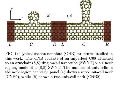
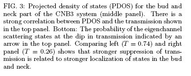
4 CARBON NANOBUDS

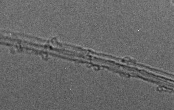
5 NanoBuds TM on FEI Titan TEM at 80kV with image C s -corrector - Movie Individual Fullerene Cluster of Fullerenes Image :B.Freitag FEI; samples : Prof. Kauppinen HUT

6 Pulling out CNBs from Hydrofobic Protein Thin Film: Fullerenes remain attached to CNTs nm X nm X175000

7 20.00 nm X nm X175000
8


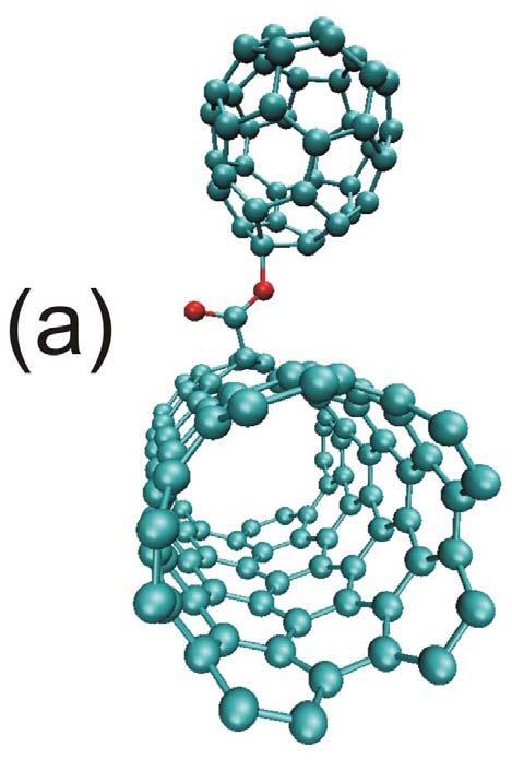
9 Bonding scenarios of fullerenes on nanotubes based on DFT calculations
10 Functionalisation of carbon nanobuds Electron transport in carbon nanobuds Transport through nanotube crossings Transport (percolation) in nanotube networks
11 Applications: Low-cost printed electronics: transistors Gas sensing
12 Tools: DFT for geometries and electronic structure Quantum transport Green s function approach - Conductance of functionalised tubes/buds - Tunnelling between crossing tubes Statistical models for percolation transport
13
14
15
16 Conductance sensitive to the bud Buds can bind gas-phase molecules Enhanced sensitivity to sensing

17 (Paula Havu, Javad Hashemi)
18
19

20

21
22

 K. Sengupta and G. Baskaran, PRB 77 (2008) 045417 Y. Gan, L. Sun, F.")
23 2. Transition metal atoms on a defected graphene sheet (Arkady Krasheninnikov) Motivations: Possible Kondo effect in graphene: the knowledge of the realistic electronic structure is required Tuning of the local electronic and magnetic structure of graphene Recent TEM experiments on migration of individual metal atoms chemisorbed on graphene T K ~ exp(-1/nj) K. Sengupta and G. Baskaran, PRB 77 (2008) Y. Gan, L. Sun, F. Banhart, Small (2008)

24 Transition metal atoms on a defected graphene sheet Further motivations : Similar to Pt, Pd, Ni, and other metal nanoparticles on carbon nanotubes, very interesting catalytic properties should be expected Understanding the interaction of transition metal atoms with sp 2 - bonded carbon is important for a better control over growth of carbon nanotubes and graphene C. Bittencourt et al., Chem. Phys. Lett. 462 (2008) 260
 Krasheninnikov et al, PRL 102 (2009)")
25 TM atoms on graphene: the simulations Spin-polarized DFT with GGA/PAW, plane waves ( VASP) Krasheninnikov et al, PRL 102 (2009)
 -0.")

, K. T. Chan et al.")
26 Transition metal adatoms on a pristine graphene sheet Fe, Co, Ni Pt Fe, spin density Au Pt Fe Co Ni E ad (ev) M ( B ) Migration barriers ev : Mobile at room temperature; Difficult to achieve control over the precise position of adatoms; The results are in agreement with several recent works: Sevincli et al., PRB 77, (2008), K. T. Chan et al., PRB 77, (2008), Suarez-Martinez et al., to be published.
 Sc Ti V Cr Mn Fe Co Ni 3d 1 4s 2 3d 2 4s 2 3d 3 4s 2 3d 5 4s 1 3d 5 4s 2 3d 6 4s 2 3d 7 4s 2 3d 8 4s 2 bond length (Å) Cu Zn Pt Au 3d 10 4s 1 3d 10 4s 2 5d 9 6s 1")
27 Metal atoms at single vacancies in graphene sheets: the structure 2.2 h The structure is not flat; TM atoms are too big to fit in elevation h (Å) Sc Ti V Cr Mn Fe Co Ni 3d 1 4s 2 3d 2 4s 2 3d 3 4s 2 3d 5 4s 1 3d 5 4s 2 3d 6 4s 2 3d 7 4s 2 3d 8 4s 2 bond length (Å) Cu Zn Pt Au 3d 10 4s 1 3d 10 4s 2 5d 9 6s 1 5d 10 6s 1 M@SV 0 M@SV
28 Metal atoms at single vacancies in graphene sheets: the bonding bond length (Å) Sc Ti V Cr Mn Fe Co Ni Cu 3d 1 4s 2 3d 2 4s 2 3d 3 4s 2 3d 5 4s 1 3d 5 4s 2 3d 6 4s 2 3d 7 4s 2 3d 8 4s 2 3d 10 4s 1 Zn Pt Au 3d 10 4s 2 5d 9 6s 1 5d 10 6s M@SV E b (ev) -8 Bonding is strong! Binding energy (<0) is the lowest for metals which form carbides Ti (3d 2 4s 2, 4 valence el.) has the lowest energy 1.7 M@SV
29 One exception: V TM atoms at double vacancies elevation h (Å) Sc Ti V Cr Mn Fe Co Ni Cu 3d 1 4s 2 3d 2 4s 2 3d 3 4s 2 3d 5 4s 1 3d 5 4s 2 3d 6 4s 2 3d 7 4s 2 3d 8 4s 2 3d 10 4s 1 bond length (Å) Zn Pt Au 3d 10 4s 2 5d 9 6s 1 5d 10 6s 1 V M@DV M@DV 0
 Sc Ti V Cr Mn Fe Co Ni Cu 3d 1 4s 2 3d 2 4s 2 3d 3 4s 2 3d 5 4s 1 3d 5 4s 2 3d 6 4s 2 3d 7 4s 2 3d 8 4s 2 3d 10 4s 1 Zn Pt Au 3d 10 4s 2 5d 9 6s 1 5d 10 6s 1-2 -4-6 E b")
30 TM atoms at double vacancies V bond length (Å) Sc Ti V Cr Mn Fe Co Ni Cu 3d 1 4s 2 3d 2 4s 2 3d 3 4s 2 3d 5 4s 1 3d 5 4s 2 3d 6 4s 2 3d 7 4s 2 3d 8 4s 2 3d 10 4s 1 Zn Pt Au 3d 10 4s 2 5d 9 6s 1 5d 10 6s E b (ev) M@DV -8 Bonding is strong, as in the case of single vacancies! V binds weakly due to two bonds only Ti and Au complexes are almost flat 1.8 M@DV
31 binding and magnetism 3 Qualitative picture E b (ev) Sc Ti V Cr Mn Fe Co Ni Cu 3d 1 4s 2 3d 2 4s 2 3d 3 4s 2 3d 5 4s 1 3d 5 4s 2 3d 6 4s 2 3d 7 4s 2 3d 8 4s 2 3d 10 4s 1 M ( B ) Zn Pt Au 3d 10 4s 2 5d 9 6s 1 5d 10 6s 1 Ti: 4 e, M=0 V: 5 e, M=1 Cr: 6 e, M=2 Mn: 7 e, M=3 Fe: 8 e, M=0: e-e repulsion -8 M@DV M@SV V


32 Magnetism: the quantitative picture Energy-resolved magnetization density Total magnetization density Both d-states of transition metal atoms and / -states of neighboring C atoms contribute to the magnetization; For Au and Cu, a considerable part of the magnetization comes from s and p states;

 elevated")
33 Mobility of complexes Nudged elastic band method, DFT GGA/PAW Au Pt Fe Co Ni experim. 2.4* * Y. Gan, L. Sun, F. Banhart, Small (2008) Naked SV ~ 1.4 ev Naked DV ~ 7 ev TM@SV complexes are be immobile at room and even moderate ( C) elevated temperatures TM@DV are immobile even at high temperatures
34 Possible experimental realization electron beam in modern TEMs can be focused onto a sub-å 2 area Knock-out of individual atoms is possible Graphene flakes with adsorbed metal atoms can be synthesized as in Y. Gan, L. Sun, F. Banhart, Small (2008) Increasing the temperature (plus e- beam sputtering of metal particles) will make the metal atoms mobile Vacancies should pin the metal atoms Focused ion beams can also be used
35 3 (a) Ferroelectric perovskites (Riku Oja, poster) General ABO 3 perovskite in the cubic (non-polarized) phase Perovskites exhibit interesting dielectric and electromechanical phenomena Applications in memories and sensors Very sensitive to small deformations, high accuracy required in DFT
36 Perovskite superlattices Charge-imbalanced interfaces may lead to 2D metallicity [1] Anomalous volume and permittivity [2] caused by interfacial ionic displacements [3] [1] A. Ohtomo et al., Nature (2002) [2] J. Narkilahti et al., Phys. Rev. B (2009) [3] R. Oja and R. M. Nieminen, Phys. Rev. B (2009) Distance (Å) Distance (Å) Distance (Å) SrO Sr-Sr Sr-Na Na-Na Na-Na Na-Na Na-Sr 3.8 Nb-Ti Ti-Nb Nb-Nb Nb-Nb Nb-Nb Nb-Nb Nb-Ti O-O2 O2-O O-O2 O2-O O-O2 O2-O O-O2 O2-O O-O2 O2-O O-O2 O2-O TiO 2 SrO n interface (NbO 2 ) + (NaO) - (NbO 2 ) + Lattice expansion: ionic distances in NaNbO 3 /SrTiO 3 superlattice with two n interfaces (NaO) - (NbO 2 ) + (NaO) - (NbO 2 ) + (NaO) - (NbO 2 ) + n interface SrO
37 Strain-induced ferroelectricity Incipient ferroelectrics may become ferroelectric when epitaxially strained In cooperation with University of Oulu, first verification of strain-induced ferroelectricity [4] 0.06 Displacement [Å] P z P=0 P xy Strain x(ta)= y(ta) x(o1)= y(o1) x(o2)= y(o3) x(o3)= y(o2) z(ta) z(o1) z(o2)= z(o3) [4] M. Tyunina, J. Narkilahti, M. Plekh, R. Oja, R. M. Nieminen, A. Dejneka, and V. Trepakov, Phys. Rev. Lett. (in press) Displacements in strained KTaO 3
38 Current studies Using hybrid functionals (B1-WC) for correct estimate of displacements and bandgaps in ferroelectrics Calculating quantum transport (tunneling) through ferroelectric layer Conductivity determined by layer thickness and perovskite-electrode interface properties Polarization direction may affect electrical conductivity if the interfaces are different [5], [6]. [5] M. Ye. Zhuravlev et al., Appl. Phys. Lett (2009) [6] V. Garcia et al., Nature (2009)
39 3 (b) Comparative Study of n-type Transparent Conductive Oxides: SnO 2, In 2 O 3, ZnO (Péter Ágoston, Karsten Albe, Martti Puska)

 C. Körber et. al.")
40 Transparent Conducting Oxides - properties Key properties: n-type conductivity Non-stoichiometry Vis-Transparency Typical Materials: ITO (In 2 O 3 :Sn) FTO (SnO 2 :F) ATO (SnO 2 :Sb) AZO (ZnO:Al) C. Körber et. al. Sensors and Actuators B (2009)


41 Transparent Conducting Oxides - applications Organic LED Thin film Solar Cell Flat Panel Display Organic solar cell Gas Sensor Low-e glass

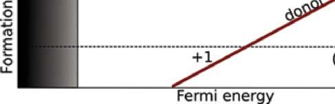
42 Defect/impurity-related ionisation levels in insulators deep donor shallow donor


43 Possibilities for n-type TCO material deep shallow resonant effective mass like


44 Possibilities for n-type TCO material Small band gap dopable not transparent Large band gap not dopable transparent


45 n-type TCO materials Wurzite Zinc Oxide Gallium Oxide Large band-gap Germanium Oxide Cadmium Oxide Bixbyite Indium Oxide Rutile Tin Oxide
46 Previous work SnO 2 Doping limit (FTO) ECMB (experiment) C. Kilic A. Zunger Phys. Rev. Lett. 88, (2002)

47 Previous work Persistent Photoconductivity (PPC) Similar behavior of ZnO and In 2 O 3 Explanation for n-type behavior S. Lany & A. Zunger Phys. Rev. Lett. 98, (2007)
48 Previous work SnO 2 Similar picture for SnO 2 No n-type behavior Hydrogen as a donor Hydrogen is everywhere and difficult to detect Singh et. al. Phys. Rev. Lett. 101, (2008)

49 Previous work: substitutional hydrogen Janotti et. al. Nature Materials. 6, (2007)


50 LDA band gap problem

51 Defect states in LDA
52 Motivation Conduction mechanism of TCO materials n- and p-type doping of TCO materials Role of stoichiometry Role of unwanted impurities Very unsatisfactory from the theoretical point of view!
53 Native defects in TCOs: computational results
54 Effect of XC-functional Inclusion of Hartree-Fock exchange into the XC-functional Hybrid Functionals PBE0 HSE06 B3LYP Hartree-Fock exchange is really non-local!
55 Methodology: Density Functional Theory Vienna ab-initio simulation package (Vasp) basis set : plane wave / periodic boundaries ion cores : projector augmented wave (PAW) V XC : HSE06, PBE0, GGA+(U), LDA, GGA U-J : 7.0 (In 2 O 3 ), 3.6 (SnO 2 ), 4.1 (ZnO) k-points : 2 x 2 x 2 MP grid (Gamma only for HF-XC) E cut : 500 ev cell sizes : 72(-750), 80(-640)
 Constant formation energies for the neutral charge state Strongly reduced formation energies for")
56 Intrinsic conductivity of n-type TCOs: role oxygen vacancies Agoston et al. Phys. Rev. Lett. 103, (2009) Constant formation energies for the neutral charge state Strongly reduced formation energies for doubly positive charge states
57 Intrinsic conductivity of n-type TCOs Defect states shift upwards with increasing complexity of XC-functional Defects remain mainly deep donors

58 Acceptor defects: compensation Stability of acceptor defects increases with increasing Fermi energy High formation energies for acceptor defects The materials are now highly n-type dopable which is not the case in LDA
59 Acceptor defects Doping limits agree with experiment for In 2 O 3 but not for SnO 2 New doping strategies for SnO 2

60 Vacancy relaxation in n-type TCOs Relaxation energy increase with the complexity of XC-functional Relaxation in neutral charge state only for ZnO
61 Cell size dependent defect state position: finite-size scaling for charged defects
62 Summary and conclusions Hybrid functionals increase the n-type propensity for TCOs The effect is due to the underestimated bandgap, ionization potential The relaxation energies are not well described in LDA/GGA LDA/GGA + U is not the way to describe these materials Oxygen vacancies are shallow donor defects in In 2 O 3 Oxygen vacancies are moderately shallow in SnO 2 Probably, additional contributions to n-type conductivity in SnO 2, ZnO Other (deep) donors in ZnO (H, PPC) cannot be excluded
This is an electronic reprint of the original article. This reprint may differ from the original in pagination and typographic detail.
 Powered by TCPDF (www.tcpdf.org) This is an electronic reprint of the original article. This reprint may differ from the original in pagination and typographic detail. Ágoston, Péter; Albe, Karsten; Nieminen,
This is an electronic reprint of the original article. This reprint may differ from the original in pagination and typographic detail.
 Powered by TCPDF (www.tcpdf.org) This is an electronic reprint of the original article. This reprint may differ from the original in pagination and typographic detail. Author(s): Krasheninnikov, A. V.
Defects and diffusion in metal oxides: Challenges for first-principles modelling
 Defects and diffusion in metal oxides: Challenges for first-principles modelling Karsten Albe, FG Materialmodellierung, TU Darmstadt Johan Pohl, Peter Agoston, Paul Erhart, Manuel Diehm FUNDING: ICTP Workshop
Defects in TiO 2 Crystals
 , March 13-15, 2013, Hong Kong Defects in TiO 2 Crystals Richard Rivera, Arvids Stashans 1 Abstract-TiO 2 crystals, anatase and rutile, have been studied using Density Functional Theory (DFT) and the Generalized
Outline. Introduction: graphene. Adsorption on graphene: - Chemisorption - Physisorption. Summary
 Outline Introduction: graphene Adsorption on graphene: - Chemisorption - Physisorption Summary 1 Electronic band structure: Electronic properties K Γ M v F = 10 6 ms -1 = c/300 massless Dirac particles!
Topological band-order transition and quantum spin Hall edge engineering in functionalized X-Bi(111) (X = Ga, In, and Tl) bilayer
 (X = Ga, In, and Tl) bilayer") Supplementary Material Topological band-order transition and quantum spin Hall edge engineering in functionalized X-Bi(111) (X = Ga, In, and Tl) bilayer Youngjae Kim, Won Seok Yun, and J. D. Lee* Department
Supplementary Material Topological band-order transition and quantum spin Hall edge engineering in functionalized X-Bi(111) (X = Ga, In, and Tl) bilayer Youngjae Kim, Won Seok Yun, and J. D. Lee* Department
Chris G. Van de Walle Materials Department, UCSB
 First-principles simulations of defects in oxides and nitrides Chris G. Van de Walle Materials Department, UCSB Acknowledgments: A. Janotti, J. Lyons, J. Varley, J. Weber (UCSB) P. Rinke (FHI), M. Scheffler
SnO 2 Physical and Chemical Properties due to the Impurity Doping
 , March 13-15, 2013, Hong Kong SnO 2 Physical and Chemical Properties due to the Impurity Doping Richard Rivera, Freddy Marcillo, Washington Chamba, Patricio Puchaicela, Arvids Stashans Abstract First-principles
Southeast University, Nanjing, China 2 Department of Applied Physics, Aalto University,
 Supplementary Information to Solubility of Boron, Carbon and Nitrogen in Transition Metals: Getting Insight into Trends from First-Principles Calculations Xiaohui Hu, 1,2 Torbjörn Björkman 2,3, Harri Lipsanen
Impurities and graphene hybrid structures: insights from first-principles theory
 Impurities and graphene hybrid structures: insights from first-principles theory Tim Wehling Institute for Theoretical Physics and Bremen Center for Computational Materials Science University of Bremen
Bound small hole polarons in oxides and related materials: strong colorations and high ionization energies
 Bound small hole polarons in oxides and related materials: strong colorations and high ionization energies O. F. Schirmer Universität Osnabrück central example: acceptor Li + Zn in ZnO O O 2 Small polaron:
New Perspectives in ab initio Calculations. Semiconducting Oxides
 for Semiconducting Oxides Volker Eyert Center for Electronic Correlations and Magnetism Institute of Physics, University of Augsburg October 28, 21 Outline LAOSTO 1 LAOSTO 2 Outline LAOSTO 1 LAOSTO 2 Calculated
SUPPLEMENTARY INFORMATION
 Atomic structure and dynamic behaviour of truly one-dimensional ionic chains inside carbon nanotubes Ryosuke Senga 1, Hannu-Pekka Komsa 2, Zheng Liu 1, Kaori Hirose-Takai 1, Arkady V. Krasheninnikov 2
Electrons, Holes, and Defect ionization
 Electrons, Holes, and Defect ionization The process of forming intrinsic electron-hole pairs is excitation a cross the band gap ( formation energy ). intrinsic electronic reaction : null e + h When electrons
What so special about LaAlO3/SrTiO3 interface? Magnetism, Superconductivity and their coexistence at the interface
 What so special about LaAlO3/SrTiO3 interface? Magnetism, Superconductivity and their coexistence at the interface Pramod Verma Indian Institute of Science, Bangalore 560012 July 24, 2014 Pramod Verma
Defects in Semiconductors
 Defects in Semiconductors Mater. Res. Soc. Symp. Proc. Vol. 1370 2011 Materials Research Society DOI: 10.1557/opl.2011. 771 Electronic Structure of O-vacancy in High-k Dielectrics and Oxide Semiconductors
Electrostatic charging and redox effects in oxide heterostructures
 Electrostatic charging and redox effects in oxide heterostructures Peter Littlewood 1,2,3 Nick Bristowe 3 & Emilio Artacho 3,6 Miguel Pruneda 4 and Massimiliano Stengel 5 1 Argonne National Laboratory
6. Computational Design of Energy-related Materials
 6. Computational Design of Energy-related Materials Contents 6.1 Atomistic Simulation Methods for Energy Materials 6.2 ab initio design of photovoltaic materials 6.3 Solid Ion Conductors for Fuel Cells
2) Atom manipulation. Xe / Ni(110) Model: Experiment:
 Atom manipulation. Xe / Ni(110) Model: Experiment:") 2) Atom manipulation D. Eigler & E. Schweizer, Nature 344, 524 (1990) Xe / Ni(110) Model: Experiment: G.Meyer, et al. Applied Physics A 68, 125 (1999) First the tip is approached close to the adsorbate
2) Atom manipulation D. Eigler & E. Schweizer, Nature 344, 524 (1990) Xe / Ni(110) Model: Experiment: G.Meyer, et al. Applied Physics A 68, 125 (1999) First the tip is approached close to the adsorbate
SCIENCE CHINA Physics, Mechanics & Astronomy. Electronic structure and optical properties of N-Zn co-doped -Ga 2 O 3
 SCIENCE CHINA Physics, Mechanics & Astronomy Article April 2012 Vol.55 No.4: 654 659 doi: 10.1007/s11433-012-4686-9 Electronic structure and optical properties of N-Zn co-doped -Ga 2 O 3 YAN JinLiang *
EE143 Fall 2016 Microfabrication Technologies. Evolution of Devices
 EE143 Fall 2016 Microfabrication Technologies Prof. Ming C. Wu wu@eecs.berkeley.edu 511 Sutardja Dai Hall (SDH) 1-1 Evolution of Devices Yesterday s Transistor (1947) Today s Transistor (2006) 1-2 1 Why
Supporting information. Realizing Two-Dimensional Magnetic Semiconductors with. Enhanced Curie Temperature by Antiaromatic Ring Based
 Supporting information Realizing Two-Dimensional Magnetic Semiconductors with Enhanced Curie Temperature by Antiaromatic Ring Based Organometallic Frameworks Xingxing Li and Jinlong Yang* Department of
Chris G. Van de Walle
 Complex oxide interfaces Chris G. Van de Walle Anderson Janotti, Lars Bjaalie, Luke Gordon, Burak Himmetoglu, K. Krishnaswamy Materials Department, University of California, Santa Barbara ES213 June 11-14,
FIRST-PRINCIPLES MODELING OF OXYGEN INTERACTION WITH ABO 3 -TYPE PEROVSKITE SURFACES
 FIRST-PRINCIPLES MODELING OF OXYGEN INTERACTION WITH ABO 3 -TYPE PEROVSKITE SURFACES S. Piskunov, E.A. Kotomin, Yu.F. Zhukovskii, and V. Alexandrov FMNT 2010, Riga, March 17 Motivation: Oxygen adsorption
From 180º stripe domains to more exotic patterns of polarization in ferroelectric nanostructures. A first principles view
 From 180º stripe domains to more exotic patterns of polarization in ferroelectric nanostructures. A first principles view Pablo Aguado-Puente Javier Junquera Ferroelectricity: Basic definitions Existence
Electronic band structure, sx-lda, Hybrid DFT, LDA+U and all that. Keith Refson STFC Rutherford Appleton Laboratory
 Electronic band structure, sx-lda, Hybrid DFT, LDA+U and all that Keith Refson STFC Rutherford Appleton Laboratory LDA/GGA DFT is good but... Naive LDA/GGA calculation severely underestimates band-gaps.
Introduction to Density Functional Theory
 1 Introduction to Density Functional Theory 21 February 2011; V172 P.Ravindran, FME-course on Ab initio Modelling of solar cell Materials 21 February 2011 Introduction to DFT 2 3 4 Ab initio Computational
Carbon Nanotubes in Interconnect Applications
 Carbon Nanotubes in Interconnect Applications Page 1 What are Carbon Nanotubes? What are they good for? Why are we interested in them? - Interconnects of the future? Comparison of electrical properties
Binding energy of 2D materials using Quantum Monte Carlo
 Quantum Monte Carlo in the Apuan Alps IX International Workshop, 26th July to 2nd August 2014 The Apuan Alps Centre for Physics @ TTI, Vallico Sotto, Tuscany, Italy Binding energy of 2D materials using
Periodic Trends in Properties of Homonuclear
 Chapter 8 Periodic Trends in Properties of Homonuclear Diatomic Molecules Up to now, we have discussed various physical properties of nanostructures, namely, two-dimensional - graphene-like structures:
Carbon Nanomaterials: Nanotubes and Nanobuds and Graphene towards new products 2030
 Carbon Nanomaterials: Nanotubes and Nanobuds and Graphene towards new products 2030 Prof. Dr. Esko I. Kauppinen Helsinki University of Technology (TKK) Espoo, Finland Forecast Seminar February 13, 2009
NANOSTRUCTURED OXIDES: NEW MATERIALS FOR ENERGY AND ENVIRONMENT
 NANOSTRUCTURED OXIDES: NEW MATERIALS FOR ENERGY AND ENVIRONMENT Quantum Chemistry Laboratory Dipartimento di Scienza dei Materiali Università Milano-Bicocca http://www.mater.unimib.it/utenti/pacchioni
Supporting Information. Designing a Lower Band Gap Bulk Ferroelectric Material with a Sizable. Polarization at Room Temperature
 Supporting Information Designing a Lower Band Gap Bulk Ferroelectric Material with a Sizable Polarization at Room Temperature Shyamashis Das, Somnath Ghara, # Priya Mahadevan, A. Sundaresan, # J. Gopalakrishnan,
EECS143 Microfabrication Technology
 EECS143 Microfabrication Technology Professor Ali Javey Introduction to Materials Lecture 1 Evolution of Devices Yesterday s Transistor (1947) Today s Transistor (2006) Why Semiconductors? Conductors e.g
METAL/CARBON-NANOTUBE INTERFACE EFFECT ON ELECTRONIC TRANSPORT
 METAL/CARBON-NANOTUBE INTERFACE EFFECT ON ELECTRONIC TRANSPORT S. Krompiewski Institute of Molecular Physics, Polish Academy of Sciences, M. Smoluchowskiego 17, 60-179 Poznań, Poland OUTLINE 1. Introductory
2D MBE Activities in Sheffield. I. Farrer, J. Heffernan Electronic and Electrical Engineering The University of Sheffield
 2D MBE Activities in Sheffield I. Farrer, J. Heffernan Electronic and Electrical Engineering The University of Sheffield Outline Motivation Van der Waals crystals The Transition Metal Di-Chalcogenides
Lecture 7: Extrinsic semiconductors - Fermi level
 Lecture 7: Extrinsic semiconductors - Fermi level Contents 1 Dopant materials 1 2 E F in extrinsic semiconductors 5 3 Temperature dependence of carrier concentration 6 3.1 Low temperature regime (T < T
Modified Becke-Johnson (mbj) exchange potential
 exchange potential") Modified Becke-Johnson (mbj) exchange potential Hideyuki Jippo Fujitsu Laboratories LTD. 2015.12.21-22 OpenMX developer s meeting @ Kobe Overview: mbj potential The semilocal exchange potential adding
Modified Becke-Johnson (mbj) exchange potential Hideyuki Jippo Fujitsu Laboratories LTD. 2015.12.21-22 OpenMX developer s meeting @ Kobe Overview: mbj potential The semilocal exchange potential adding
Vacancies in CuInSe(2): new insights from hybrid-functional calculations
: new insights from hybrid-functional calculations") Zurich Open Repository and Archive University of Zurich Main Library Strickhofstrasse 39 CH-8057 Zurich www.zora.uzh.ch Year: 2011 Vacancies in CuInSe(2): new insights from hybrid-functional calculations
Zurich Open Repository and Archive University of Zurich Main Library Strickhofstrasse 39 CH-8057 Zurich www.zora.uzh.ch Year: 2011 Vacancies in CuInSe(2): new insights from hybrid-functional calculations
Publication I. c 2010 American Physical Society. Reprinted with permission.
 Publication I Tyunina, M., Narkilahti, J., Plekh, M., Oja, R., Nieminen, R.M., Dejneka, A., and Trepakov, V. Evidence for Strain-Induced Ferroelectric Order in Epitaxial Thin-Film KTaO 3. Physical Review
Supplementary Information
 Supplementary Information Supplementary Figure 1: Electronic Kohn-Sham potential profile of a charged monolayer MoTe 2 calculated using PBE-DFT. Plotted is the averaged electronic Kohn- Sham potential
Part II Electrical Properties of Materials
 Part II Electrical Properties of Materials Chap. 7 Electrical Conduction in Metals and Alloys Chap. 8 Semiconductors Chap. 9 9.1 Conducting Polymers and Organic Metals Polymers consist of (macro)molecules
A semiconductor is an almost insulating material, in which by contamination (doping) positive or negative charge carriers can be introduced.
 positive or negative charge carriers can be introduced.") Semiconductor A semiconductor is an almost insulating material, in which by contamination (doping) positive or negative charge carriers can be introduced. Page 2 Semiconductor materials Page 3 Energy levels
Semiconductor A semiconductor is an almost insulating material, in which by contamination (doping) positive or negative charge carriers can be introduced. Page 2 Semiconductor materials Page 3 Energy levels
Chapter 1 Overview of Semiconductor Materials and Physics
 Chapter 1 Overview of Semiconductor Materials and Physics Professor Paul K. Chu Conductivity / Resistivity of Insulators, Semiconductors, and Conductors Semiconductor Elements Period II III IV V VI 2 B
Transparent Electrode Applications
 Transparent Electrode Applications LCD Solar Cells Touch Screen Indium Tin Oxide (ITO) Zinc Oxide (ZnO) - High conductivity - High transparency - Resistant to environmental effects - Rare material (Indium)
Crystal Properties. MS415 Lec. 2. High performance, high current. ZnO. GaN
 Crystal Properties Crystal Lattices: Periodic arrangement of atoms Repeated unit cells (solid-state) Stuffing atoms into unit cells Determine mechanical & electrical properties High performance, high current
The Semiconductor in Equilibrium
 Lecture 6 Semiconductor physics IV The Semiconductor in Equilibrium Equilibrium, or thermal equilibrium No external forces such as voltages, electric fields. Magnetic fields, or temperature gradients are
per unit cell Motif: Re at (0, 0, 0); 3O at ( 1 / 2, 0), (0, 0, 1 / 2 ) Re: 6 (octahedral coordination) O: 2 (linear coordination) ReO 6
; 3O at ( 1 / 2, 0), (0, 0, 1 / 2 ) Re: 6 (octahedral coordination) O: 2 (linear coordination) ReO 6") Lattice: Primitive Cubic 1ReO 3 per unit cell Motif: Re at (0, 0, 0); 3O at ( 1 / 2, 0, 0), (0, 1 / 2, 0), (0, 0, 1 / 2 ) Re: 6 (octahedral coordination) O: 2 (linear coordination) ReO 6 octahedra share
Lattice: Primitive Cubic 1ReO 3 per unit cell Motif: Re at (0, 0, 0); 3O at ( 1 / 2, 0, 0), (0, 1 / 2, 0), (0, 0, 1 / 2 ) Re: 6 (octahedral coordination) O: 2 (linear coordination) ReO 6 octahedra share
Teoría del Funcional de la Densidad (Density Functional Theory)
") Teoría del Funcional de la Densidad (Density Functional Theory) Motivation: limitations of the standard approach based on the wave function. The electronic density n(r) as the key variable: Functionals
Teoría del Funcional de la Densidad (Density Functional Theory) Motivation: limitations of the standard approach based on the wave function. The electronic density n(r) as the key variable: Functionals
Functionalized Carbon Nanotubes a key to nanotechnology?
 1 27th Max Born Symposium Multiscale Modeling of Real Materials Wroclaw, Sep 19, 2010 Functionalized Carbon Nanotubes a key to nanotechnology? Karolina Milowska, Magda Birowska & Jacek A. Majewski Faculty
arxiv: v1 [cond-mat.mes-hall] 15 Aug 2014
![arxiv: v1 [cond-mat.mes-hall] 15 Aug 2014](/thumbs/89/97831186.jpg "arxiv: v1 [cond-mat.mes-hall] 15 Aug 2014") The potential applications of phosphorene as anode arxiv:1408.3488v1 [cond-mat.mes-hall] 15 Aug 2014 materials in Li-ion batteries Shijun Zhao,, and Wei Kang, HEDPS, Center for Applied Physics and Technology,
The potential applications of phosphorene as anode arxiv:1408.3488v1 [cond-mat.mes-hall] 15 Aug 2014 materials in Li-ion batteries Shijun Zhao,, and Wei Kang, HEDPS, Center for Applied Physics and Technology,
Supporting Information
 Supporting Information Controlled Growth of Ceria Nanoarrays on Anatase Titania Powder: A Bottom-up Physical Picture Hyun You Kim 1, Mark S. Hybertsen 2*, and Ping Liu 2* 1 Department of Materials Science
Oxide Interfaces: Perspectives & New Physics
 Oxide Interfaces: Perspectives & New Physics Seminar, University of Illinois September 24, 2007 Sashi Satpathy University of Missouri, Columbia Funding: DOE, AFOSR, PRF, MURB, DFG http://www.missouri.edu/~satpathys
Supporting Information for: Capacitive Sensing of Intercalated H2O Molecules Using Graphene
 Supporting Information for: Capacitive Sensing of Intercalated H2O Molecules Using Graphene Eric J. Olson, Rui Ma, Tao Sun, Mona A. Ebrish, Nazila Haratipour, Kyoungmin Min, Narayana R. Aluru, and Steven
Design of Efficient Catalysts with Double Transition Metal. Atoms on C 2 N Layer
 Supporting Information Design of Efficient Catalysts with Double Transition Metal Atoms on C 2 N Layer Xiyu Li, 1, Wenhui Zhong, 2, Peng Cui, 1 Jun Li, 1 Jun Jiang 1, * 1 Hefei National Laboratory for
Self-compensating incorporation of Mn in Ga 1 x Mn x As
 Self-compensating incorporation of Mn in Ga 1 x Mn x As arxiv:cond-mat/0201131v1 [cond-mat.mtrl-sci] 9 Jan 2002 J. Mašek and F. Máca Institute of Physics, Academy of Sciences of the CR CZ-182 21 Praha
Origin of Metallic States at Heterointerface between Band Insulators LaAlO 3 and SrTiO 3
 Origin of Metallic States at Heterointerface between Band Insulators LaAlO 3 and SrTiO 3 K. Yoshimatsu 1, R. Yasuhara 1, H. Kumigashira 1, 2, *, and M. Oshima 1, 2 1 Department of Applied Chemistry, University
Supplemental Material: Experimental and Theoretical Investigations of the Electronic Band Structure of Metal-Organic Framework of HKUST-1 Type
 Supplemental Material: Experimental and Theoretical Investigations of the Electronic Band Structure of Metal-Organic Framework of HKUST-1 Type Zhigang Gu, a Lars Heinke, a,* Christof Wöll a, Tobias Neumann,
Chapter 10: Modern Atomic Theory and the Periodic Table. How does atomic structure relate to the periodic table? 10.1 Electromagnetic Radiation
 Chapter 10: Modern Atomic Theory and the Periodic Table How does atomic structure relate to the periodic table? 10.1 Electromagnetic Radiation Electromagnetic (EM) radiation is a form of energy that exhibits
Transport through Andreev Bound States in a Superconductor-Quantum Dot-Graphene System
 Transport through Andreev Bound States in a Superconductor-Quantum Dot-Graphene System Nadya Mason Travis Dirk, Yung-Fu Chen, Cesar Chialvo Taylor Hughes, Siddhartha Lal, Bruno Uchoa Paul Goldbart University
Direct and Indirect Semiconductor
 Direct and Indirect Semiconductor Allowed values of energy can be plotted vs. the propagation constant, k. Since the periodicity of most lattices is different in various direction, the E-k diagram must
Polar oxide surfaces and ultra-thin films
 Polar oxide surfaces and ultra-thin films Claudine Noguera Institut des Nanosciences de Paris, CNRS UMR 7588, Université Pierre et Marie Curie (Paris VI) Campus de Boucicaut, 140 rue Lourmel, 75015 Paris
Chapter 4: Bonding in Solids and Electronic Properties. Free electron theory
 Chapter 4: Bonding in Solids and Electronic Properties Free electron theory Consider free electrons in a metal an electron gas. regards a metal as a box in which electrons are free to move. assumes nuclei
Basics of DFT applications to solids and surfaces
 Basics of DFT applications to solids and surfaces Peter Kratzer Physics Department, University Duisburg-Essen, Duisburg, Germany E-mail: Peter.Kratzer@uni-duisburg-essen.de Periodicity in real space and
Electric displacement as the fundamental variable in electronic-structure calculations
 Electric displacement as the fundamental variable in electronic-structure calculations CECAM - Centre Européen de Calcul Atomique et Moléculaire EPF Lausanne, Switzerland Conference UC Davis, 6/23/2009
Carbon based Nanoscale Electronics
 Carbon based Nanoscale Electronics 09 02 200802 2008 ME class Outline driving force for the carbon nanomaterial electronic properties of fullerene exploration of electronic carbon nanotube gold rush of
Silicon vacancy in SiC: A high-spin state defect
 Powered by TCPDF (www.tcpdf.org) This is an electronic reprint of the original article. This reprint may differ from the original in pagination and typographic detail. Author(s): Torpo, L. & Nieminen,
Introduction to Density Functional Theory with Applications to Graphene Branislav K. Nikolić
 Introduction to Density Functional Theory with Applications to Graphene Branislav K. Nikolić Department of Physics and Astronomy, University of Delaware, Newark, DE 19716, U.S.A. http://wiki.physics.udel.edu/phys824
Microscopical and Microanalytical Methods (NANO3)
") Microscopical and Microanalytical Methods (NANO3) 06.11.15 10:15-12:00 Introduction - SPM methods 13.11.15 10:15-12:00 STM 20.11.15 10:15-12:00 STS Erik Zupanič erik.zupanic@ijs.si stm.ijs.si 27.11.15
Microscopical and Microanalytical Methods (NANO3) 06.11.15 10:15-12:00 Introduction - SPM methods 13.11.15 10:15-12:00 STM 20.11.15 10:15-12:00 STS Erik Zupanič erik.zupanic@ijs.si stm.ijs.si 27.11.15
Defects in materials. Manish Jain. July 8, Department of Physics Indian Institute of Science Bangalore 1/46
 1/46 Defects in materials Manish Jain Department of Physics Indian Institute of Science Bangalore July 8, 2014 Outline 2/46 Motivation. Computational methods. Defects in oxides. Why are defects challenging?
Semi-insulating SiC substrates for high frequency devices
 Klausurtagung Silberbach, 19. - 21. Feb. 2002 Institut für Werkstoffwissenschaften - WW 6 Semi-insulating SiC substrates for high frequency devices Vortrag von Matthias Bickermann Semi-insulating SiC substrates
STM spectroscopy (STS)
") STM spectroscopy (STS) di dv 4 e ( E ev, r) ( E ) M S F T F Basic concepts of STS. With the feedback circuit open the variation of the tunneling current due to the application of a small oscillating voltage
STM spectroscopy (STS) di dv 4 e ( E ev, r) ( E ) M S F T F Basic concepts of STS. With the feedback circuit open the variation of the tunneling current due to the application of a small oscillating voltage
Challenges and Opportunities. Prof. J. Raynien Kwo 年
 Nanoelectronics Beyond Si: Challenges and Opportunities Prof. J. Raynien Kwo 年 立 Si CMOS Device Scaling Beyond 22 nm node High κ,, Metal gates, and High mobility channel 1947 First Transistor 1960 1960
 lectures accompanying the book: Solid State Physics: An Introduction, by Philip ofmann (2nd edition 2015, ISBN-10: 3527412824, ISBN-13: 978-3527412822, Wiley-VC Berlin. www.philiphofmann.net 1 Bonds between
Interaction between a single-molecule
 Interaction between a single-molecule magnet Mn 12 monolayer and a gold surface 12 Kyungwha Park Department of Physics, Virginia Tech Salvador Barraza-Lopez (postdoc) Michael C. Avery (undergraduate) Supported
R measurements (resistivity, magnetoresistance, Hall). Makariy A. Tanatar
. Makariy A. Tanatar") R measurements (resistivity, magnetoresistance, Hall). 590B Makariy A. Tanatar April 18, 2014 Resistivity Typical resistivity temperature dependence: metals, semiconductors Magnetic scattering Resistivities
R measurements (resistivity, magnetoresistance, Hall). 590B Makariy A. Tanatar April 18, 2014 Resistivity Typical resistivity temperature dependence: metals, semiconductors Magnetic scattering Resistivities
A COMPUTATIONAL INVESTIGATION OF MIGRATION ENTHALPIES AND ELECTRONIC STRUCTURE IN SrFeO 3-δ
 A COMPUTATIONAL INVESTIGATION OF MIGRATION ENTHALPIES AND ELECTRONIC STRUCTURE IN SrFeO 3-δ A. Predith and G. Ceder Massachusetts Institute of Technology Department of Materials Science and Engineering
Computational discovery of p-type transparent oxide semiconductors using
 Computational discovery of p-type transparent oxide semiconductors using hydrogen descriptor Kanghoon Yim 1,*,, Yong Youn 1,*, Miso Lee 1, Dongsun Yoo 1, Joohee Lee 1, Sung Haeng Cho 2 & Seungwu Han 1
(a) (b) Supplementary Figure 1. (a) (b) (a) Supplementary Figure 2. (a) (b) (c) (d) (e)
 (b) Supplementary Figure 1. (a) (b) (a) Supplementary Figure 2. (a) (b) (c) (d) (e)") (a) (b) Supplementary Figure 1. (a) An AFM image of the device after the formation of the contact electrodes and the top gate dielectric Al 2 O 3. (b) A line scan performed along the white dashed line
(a) (b) Supplementary Figure 1. (a) An AFM image of the device after the formation of the contact electrodes and the top gate dielectric Al 2 O 3. (b) A line scan performed along the white dashed line
Stable Ferromagnetism and Half-metallicity in Two-Dimensional. Polyporphyrin Frameworks
 Supporting Information for Stable Ferromagnetism and Half-metallicity in Two-Dimensional Polyporphyrin Frameworks Jie Tan, a Weifeng Li, b Xiujie He, a Mingwen Zhao a,* a School of Physics and State Key
Magnetism in transition metal oxides by post-dft methods
 Magnetism in transition metal oxides by post-dft methods Cesare Franchini Faculty of Physics & Center for Computational Materials Science University of Vienna, Austria Workshop on Magnetism in Complex
Ferromagnetism and Anomalous Hall Effect in Graphene
 Ferromagnetism and Anomalous Hall Effect in Graphene Jing Shi Department of Physics & Astronomy, University of California, Riverside Graphene/YIG Introduction Outline Proximity induced ferromagnetism Quantized
Initial Stages of Growth of Organic Semiconductors on Graphene
 Initial Stages of Growth of Organic Semiconductors on Graphene Presented by: Manisha Chhikara Supervisor: Prof. Dr. Gvido Bratina University of Nova Gorica Outline Introduction to Graphene Fabrication
Low pressure CO 2 hydrogenation to methanol over gold nanoparticles activated on a CeO x /TiO 2 interface
 Low pressure CO 2 hydrogenation to methanol over gold nanoparticles activated on a CeO x /TiO 2 interface 1 Xiaofang Yang, 1 Shyam Kattel, 1 Sanjaya D. Senanayake, 2 J. Anibal Boscoboinik, 3 Xiaowa Nie,
Band calculations: Theory and Applications
 Band calculations: Theory and Applications Lecture 2: Different approximations for the exchange-correlation correlation functional in DFT Local density approximation () Generalized gradient approximation
ELECTRONIC I Lecture 1 Introduction to semiconductor. By Asst. Prof Dr. Jassim K. Hmood
 ELECTRONIC I Lecture 1 Introduction to semiconductor By Asst. Prof Dr. Jassim K. Hmood SOLID-STATE ELECTRONIC MATERIALS Electronic materials generally can be divided into three categories: insulators,
Pakpoom Reunchan. Curriculum Vitae
 Pakpoom Reunchan Curriculum Vitae Department of Physics Faculty of Science, Kasetsart University Bangkok Thailand 10900 E-mail: p.reunchan@gmail.com pakpoom.r@ku.ac.th Tel: (+66) 2-562-5555 #3048 Educations
The effect of point defects in zircon
 aterials for nuclear waste immobilization: The effect of point defects in zircon iguel Pruneda Department of Earth Sciences University of Centre for Ceramic Immobilisation Radiation damage process α-decay
GECP Hydrogen Project: "Nanomaterials Engineering for Hydrogen Storage"
 GECP Hydrogen Project: "Nanomaterials Engineering for Hydrogen Storage" PI: KJ Cho Students and Staff Members: Zhiyong Zhang, Wei Xiao, Byeongchan Lee, Experimental Collaboration: H. Dai, B. Clemens, A.
Nanotechnology and Solar Energy. Solar Electricity Photovoltaics. Fuel from the Sun Photosynthesis Biofuels Split Water Fuel Cells
 Nanotechnology and Solar Energy Solar Electricity Photovoltaics Fuel from the Sun Photosynthesis Biofuels Split Water Fuel Cells Solar cell A photon from the Sun generates an electron-hole pair in a semiconductor.
The many forms of carbon
 The many forms of carbon Carbon is not only the basis of life, it also provides an enormous variety of structures for nanotechnology. This versatility is connected to the ability of carbon to form two
Supporting Information
 Supporting Information The Origin of Active Oxygen in a Ternary CuO x /Co 3 O 4 -CeO Catalyst for CO Oxidation Zhigang Liu, *, Zili Wu, *, Xihong Peng, ++ Andrew Binder, Songhai Chai, Sheng Dai *,, School
Catalytic Activity of IrO 2 (110) Surface: A DFT study
 Surface: A DFT study") Catalytic Activity of IrO 2 (110) Surface: A DFT study Jyh-Chiang Jiang Department of Chemical Engineering, National Taiwan University of Science and Technology (NTUST) NCTS-NCKU 9/7, 2010 Computational
Catalytic Activity of IrO 2 (110) Surface: A DFT study Jyh-Chiang Jiang Department of Chemical Engineering, National Taiwan University of Science and Technology (NTUST) NCTS-NCKU 9/7, 2010 Computational
Supporting Information
 Electronic Supplementary Material (ESI) for Nanoscale. This journal is The Royal Society of Chemistry 2015 Supporting Information Single Layer Lead Iodide: Computational Exploration of Structural, Electronic
Lecture 2 Electrons and Holes in Semiconductors
 EE 471: Transport Phenomena in Solid State Devices Spring 2018 Lecture 2 Electrons and Holes in Semiconductors Bryan Ackland Department of Electrical and Computer Engineering Stevens Institute of Technology
First-principles Studies of Formaldehyde Molecule Adsorption on Graphene Modified with Vacancy, -OH, -CHO and -COOH Group
 2017 Asia-Pacific Engineering and Technology Conference (APETC 2017) ISBN: 978-1-60595-443-1 First-principles Studies of Formaldehyde Molecule Adsorption on Graphene Modified with Vacancy, -OH, -CHO and
Introduction to DFT and its Application to Defects in Semiconductors
 Introduction to DFT and its Application to Defects in Semiconductors Noa Marom Physics and Engineering Physics Tulane University New Orleans The Future: Computer-Aided Materials Design Can access the space
Solutions for Assignment-8
 Solutions for Assignment-8 Q1. The process of adding impurities to a pure semiconductor is called: [1] (a) Mixing (b) Doping (c) Diffusing (d) None of the above In semiconductor production, doping intentionally
Electronic excitations in materials for solar cells
 Electronic excitations in materials for solar cells beyond standard density functional theory Silvana Botti 1 LSI, École Polytechnique-CNRS-CEA, Palaiseau, France 2 LPMCN, CNRS-Université Lyon 1, France
Diamond. Covalent Insulators and Semiconductors. Silicon, Germanium, Gray Tin. Chem 462 September 24, 2004
 Covalent Insulators and Chem 462 September 24, 2004 Diamond Pure sp 3 carbon All bonds staggered- ideal d(c-c) - 1.54 Å, like ethane Silicon, Germanium, Gray Tin Diamond structure Si and Ge: semiconductors