per unit cell Motif: Re at (0, 0, 0); 3O at ( 1 / 2, 0), (0, 0, 1 / 2 ) Re: 6 (octahedral coordination) O: 2 (linear coordination) ReO 6
|
|
|
- Melina Bradley
- 5 years ago
- Views:
Transcription
, (0, 0, 1 / 2 ) Re: 6 (octahedral coordination) O: 2 (linear coordination)")
 Examples: WO 3, AlF 3, ScF 3, FeF 3, CoF 3, Sc(OH) 3")
1 Lattice: Primitive Cubic 1ReO 3 per unit cell Motif: Re at (0, 0, 0); 3O at ( 1 / 2, 0, 0), (0, 1 / 2, 0), (0, 0, 1 / 2 ) Re: 6 (octahedral coordination) O: 2 (linear coordination) ReO 6 octahedra share only vertices May be regarded as ccp oxide with 1 / 4 of ccp sites vacant (at center of the cell) Examples: WO 3, AlF 3, ScF 3, FeF 3, CoF 3, Sc(OH) 3 (distorted) 1
 Ti 6-coordinate by O (octahedral) O distorted octahedral (4xCa + 2xTi) TiO 6 octahedra share only vertices CaO 12 cuboctahedra share faces Ca fills the vacant ccp")
2 Lattice: Primitive Cubic (idealised structure) 1CaTiO 3 per unit cell A-Cell Motif: Ti at (0, 0, 0); Ca at ( 1 / 2, 1 / 2, 1 / 2 ); 3O at ( 1 / 2, 0, 0), (0, 1 / 2, 0), (0, 0, 1 / 2 ) Ca 12-coordinate by O (cuboctahedral) Ti 6-coordinate by O (octahedral) O distorted octahedral (4xCa + 2xTi) TiO 6 octahedra share only vertices CaO 12 cuboctahedra share faces Ca fills the vacant ccp site in ReO 3, a CaO 3 ccp arrangement with 1 / 4 of octahedral holes (those defined by 6xO) filled by Ti Examples: NaNbO 3, BaTiO 3, CaZrO 3, YAlO 3, KMgF 3 Many undergo small distortions: e.g. BaTiO 3 is ferroelectric 2

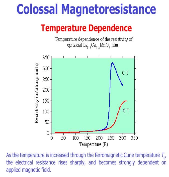
3 B X A Perovskite Structure: ABO3 Tolerance factor: t R R A X 2( RB RX ) t Effect Possible structure >1 A cation too large to fit in Hexagonal perovskite interstices ideal Cubic perovskite A cation too small Orthorhombic perovskite <0.71 A cation same size as B cation Possible close packed lattice Perovskite: most widely studied oxide structure Wide range of chemistries possible - thousands of examples known Unique properties of perovskites: - high T c cuprate superconductors - Colossal Magneto-Resistance (La,SrMnO 3 ) - fast ion conduction (Li +, O 2- ), batteries, fuel cells - mixed electronic/ionic conduction, fuel cells - oxidation/reduction catalysts - ferroelectric / piezoelectric ceramics (BaTiO 3, Pb(ZrTi)O 3 ) - important mineral structure in lower mantle (MgSiO 3 ) - frequency filters for wireless communications : Ba(Zn 1/3 Ta 2/3 )O 3 3

4 Ferroelectrics BaTiO3: Ba 2+ Ti 4+ O 2- r=1.56 Å r=0.75 Å r=1.26 Å t=0.992 KNbO3 K Å Nb Å t=1.01 LiNbO3 Li Å Nb Å t=0.81 Rhombhedral distortion 4

5 Magnetoresistive materials: LaMnO3 : 1.30 Å ; 0.72 Å t=0.91 La0.5Sr0.5MnO3: 1.28 Å, Å t=0.92 Mn 3+, d 4 : large Jahn-Teller effect, tetragonal distortion 5
6 6
7 7
8 Electronic Structure of Solids Band Theory Reading: MT 7, DG 7 8
9 Si NW 9
10 10


11 Silicon vs. Diamond CARBON Allotropes Carbon shows both Layer and Cage Networks 11

12 Synthesis of C60: Laser Ablation Arc-discharge 12


13 Smalley, Kroto, Curl 1996, Nobel prize 13

14 Carbon nanotube, 1991, NEC's Fundamental Research Laboratories 14


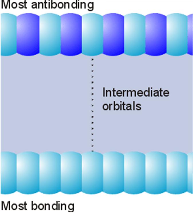
15 Discovery of Graphene Andre Geim and Konstantin Novoselov Nobel prize in Physics, u Antibonding 1 g Relative non-bonding g Slightly bonding 1 u 1 u Relative non-bonding Slightly antibonding 1 g bonding 15
16 16
17 17
18 18
19 CnHn+2 19
20 Metal Metallic Hydrogen 20

21 In extended solid, each atomic/molecular orbtial will develop into one band! Sodium According to Band Theory Conduction band: empty 3s antibonding No gap Valence band: full 3s bonding
22 Conduction Band Fermi Level Valence bond 22

23 Bonding in Metals The electron-sea model is a simple depiction of a metal as an array of positive ions surrounded by delocalized valence electrons. Metals are good conductors of electricity because of the mobility of these delocalized valence electrons. A metal also conducts heat well because the mobile electrons can carry additional kinetic energy. 180 Bonding in Metals
24 Bonding in Metals Molecular orbital theory gives a more detailed picture of the bonding in metals. According to band theory, the electrons in a crystal become free to move when they are excited to the unoccupied orbitals of a band. In a metal, this requires little energy since the unoccupied orbitals lie just above the occupied orbitals of highest energy. 182 Semiconductor 24

25 Conduction Band Valence bond Graphite Graphite has a layered structure, in which the carbon atoms in each layer bond to three other carbons with sp 2 orbitals. Of the covalent network solids, only graphite conducts electricity. This is due to the delocalization of the resonant electrons in graphite s sp 2 hybridization
26 Structure of Diamond 186 Solids: Conductors, Insulators and Semiconductors Graphite Diamond No gap Band gap = 5.5 ev 530 kj/mol Conductor Insulator

27 Solids: Conductors, Insulators and Semiconductors Band Gap for Semiconductors Diamond Si Ge 5.5 ev 1.1 ev 0.67 ev Band gap Semiconductor 188 Fullerenes The fullerenes are a family of molecules with a closed cage of carbon atoms arranged in pentagons and hexagons. Each carbon is sp 2 hybridized. The most symmetrical member is buckminsterfullerene, C 60. Buckminsterfullerenes show potential for applications in superconductivity and catalytic activity
28 28
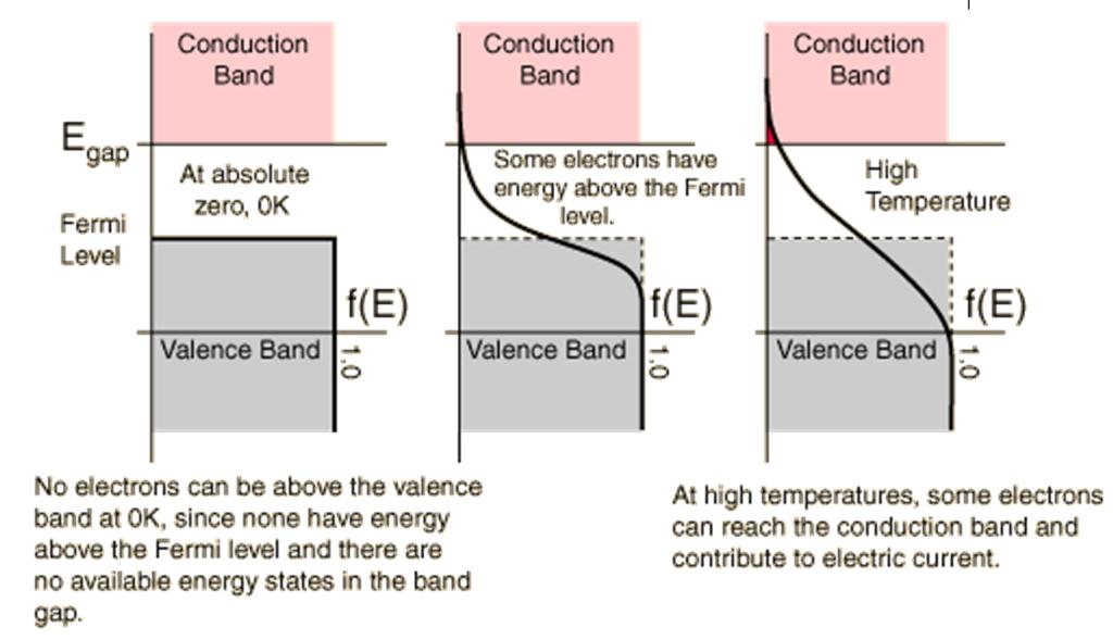
29 Fermi Level EF corresponds to the highest occupied energy at T=0 (HOMO energy) Fermi-Dirac distribution P 1 ( E E )/ kt e F 1 population P of the valence band orbitals. 29
30 Conduction Band Valence bond Fermi-Dirac distribution: f ( E) exp[( E 1 E ) / k F B T ] 1 30
31 31
32 Semiconductors Semiconducting elements form the basis of solid state electronic devices. When silicon is doped with phosphorus, it becomes an n-type semiconductor, in which electric current is carried by electrons


33 Doping in semiconductor: n-type Carrier type: electron Semiconductors Semiconducting elements form the basis of solid state electronic devices. When silicon is doped with boron, it becomes a p-type semiconductor, in which an electrical current is carried by positively charged holes


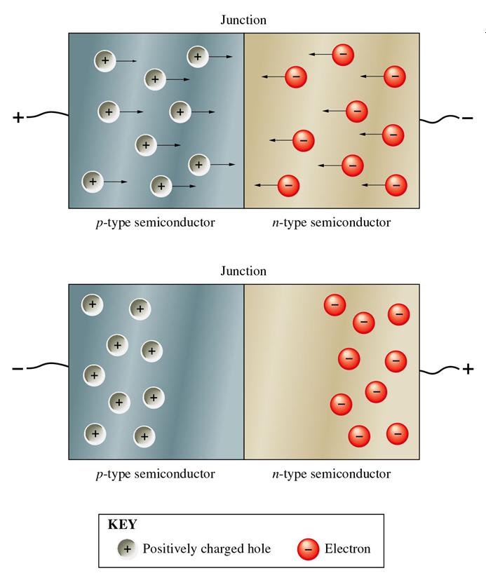
34 Doping in semiconductor: p-type Carrier type: Hole Semiconductors Semiconducting elements form the basis of solid state electronic devices. Joining a p-type semiconductor to an n- type semiconductor produces a p-n junction, which can function as a rectifier. A rectifier is a device that allows current to flow in one direction, but not the other

35

 Near IR GaP:N (E g = 2.25 ev) Yellow GaP:Zn,O (E g = 2.")
36 Light Emitting Diodes Forward bias at a p-n junction forces minority carriers across the junction. This causes electrons to fall into vacant holes radiatively, giving off light. Dopants are important sites for localizing carriers, thus transitions are often CB acceptor, or donor VB Common LED materials GaAs (E g =1.43 ev) Near IR GaP:N (E g = 2.25 ev) Yellow GaP:Zn,O (E g = 2.25 ev) Red GaN, SiC, ZnO, AlN Blue, UV 2014 Nobel Prize in physics 36
 Yellow GaP:Zn,O (E g = 2.")
37 Common LED materials GaAs (E g =1.43 ev) Near IR GaP:N (E g = 2.25 ev) Yellow GaP:Zn,O (E g = 2.25 ev) Red GaN, SiC, ZnO, AlN Blue, UV 37
Followed by metals and inert gases - close-packed structures Deviations: BCC metals 'Ionic' compounds strive to follow the principles.
 Reading: West 7 &8 Principles of Laves 1.Space Principle: Space is used most efficiently 2.Symmetry Principle: Highest possible symmetry is adopted 3.Connection Principle: There will be the most possible
Chemistry Instrumental Analysis Lecture 8. Chem 4631
 Chemistry 4631 Instrumental Analysis Lecture 8 UV to IR Components of Optical Basic components of spectroscopic instruments: stable source of radiant energy transparent container to hold sample device
ELEMENTARY BAND THEORY
 ELEMENTARY BAND THEORY PHYSICIST Solid state band Valence band, VB Conduction band, CB Fermi energy, E F Bloch orbital, delocalized n-doping p-doping Band gap, E g Direct band gap Indirect band gap Phonon
So why is sodium a metal? Tungsten Half-filled 5d band & half-filled 6s band. Insulators. Interaction of metals with light?
 Bonding in Solids: Metals, Insulators, & CHEM 107 T. Hughbanks Delocalized bonding in Solids Think of a pure solid as a single, very large molecule. Use our bonding pictures to try to understand properties.
Lecture 1. OUTLINE Basic Semiconductor Physics. Reading: Chapter 2.1. Semiconductors Intrinsic (undoped) silicon Doping Carrier concentrations
 silicon Doping Carrier concentrations") Lecture 1 OUTLINE Basic Semiconductor Physics Semiconductors Intrinsic (undoped) silicon Doping Carrier concentrations Reading: Chapter 2.1 EE105 Fall 2007 Lecture 1, Slide 1 What is a Semiconductor? Low
Lecture 1 OUTLINE Basic Semiconductor Physics Semiconductors Intrinsic (undoped) silicon Doping Carrier concentrations Reading: Chapter 2.1 EE105 Fall 2007 Lecture 1, Slide 1 What is a Semiconductor? Low
Important crystal structures: Perovskite structure. 5/29/2013 L.Viciu ACII Perovkite structure
 Important crystal structures: Perovskite structure 1 A. Structures derived from cubic close packed 1. NaCl- rock salt 2. CaF 2 fluorite/na 2 O- antifluorite 3. diamond 4. ZnS- blende B. Structures derived
Review of Semiconductor Fundamentals
 ECE 541/ME 541 Microelectronic Fabrication Techniques Review of Semiconductor Fundamentals Zheng Yang (ERF 3017, email: yangzhen@uic.edu) Page 1 Semiconductor A semiconductor is an almost insulating material,
Ga and P Atoms to Covalent Solid GaP
 Ga and P Atoms to Covalent Solid GaP Band Gaps in Binary Group III-V Semiconductors Mixed Semiconductors Affect of replacing some of the As with P in GaAs Band Gap (ev) (nm) GaAs 1.35 919 (IR) GaP 2.24
A semiconductor is an almost insulating material, in which by contamination (doping) positive or negative charge carriers can be introduced.
 positive or negative charge carriers can be introduced.") Semiconductor A semiconductor is an almost insulating material, in which by contamination (doping) positive or negative charge carriers can be introduced. Page 2 Semiconductor materials Page 3 Energy levels
Semiconductor A semiconductor is an almost insulating material, in which by contamination (doping) positive or negative charge carriers can be introduced. Page 2 Semiconductor materials Page 3 Energy levels
EE143 Fall 2016 Microfabrication Technologies. Evolution of Devices
 EE143 Fall 2016 Microfabrication Technologies Prof. Ming C. Wu wu@eecs.berkeley.edu 511 Sutardja Dai Hall (SDH) 1-1 Evolution of Devices Yesterday s Transistor (1947) Today s Transistor (2006) 1-2 1 Why
David J. Starling Penn State Hazleton PHYS 214
 Being virtually killed by a virtual laser in a virtual space is just as effective as the real thing, because you are as dead as you think you are. -Douglas Adams, Mostly Harmless David J. Starling Penn
CH676 Physical Chemistry: Principles and Applications. CH676 Physical Chemistry: Principles and Applications
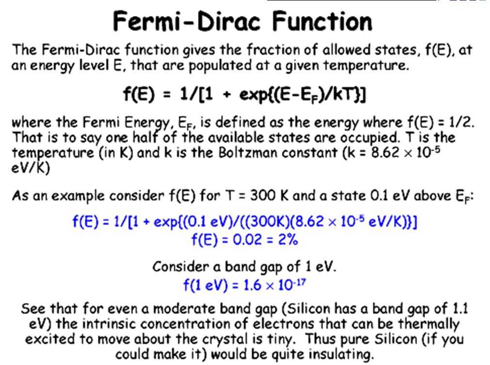
 CH676 Physical Chemistry: Principles and Applications Band Theory Fermi-Dirac Function f(e) = 1/[1 + e (E-E F)/kT ] Where the Fermi Energy, E F, is defined as the energy where f(e) = 1/2. That is to say
Electrons, Holes, and Defect ionization
 Electrons, Holes, and Defect ionization The process of forming intrinsic electron-hole pairs is excitation a cross the band gap ( formation energy ). intrinsic electronic reaction : null e + h When electrons
Carbon nanomaterials. Gavin Lawes Wayne State University.
 Carbon nanomaterials Gavin Lawes Wayne State University glawes@wayne.edu Outline 1. Carbon structures 2. Carbon nanostructures 3. Potential applications for Carbon nanostructures Periodic table from bpc.edu
Ch. 2: Energy Bands And Charge Carriers In Semiconductors
 Ch. 2: Energy Bands And Charge Carriers In Semiconductors Discrete energy levels arise from balance of attraction force between electrons and nucleus and repulsion force between electrons each electron
Basic cell design. Si cell
 Basic cell design Si cell 1 Concepts needed to describe photovoltaic device 1. energy bands in semiconductors: from bonds to bands 2. free carriers: holes and electrons, doping 3. electron and hole current:
Chapter 1 Overview of Semiconductor Materials and Physics
 Chapter 1 Overview of Semiconductor Materials and Physics Professor Paul K. Chu Conductivity / Resistivity of Insulators, Semiconductors, and Conductors Semiconductor Elements Period II III IV V VI 2 B
smal band gap Saturday, April 9, 2011
 small band gap upper (conduction) band empty small gap valence band filled 2s 2p 2s 2p hybrid (s+p)band 2p no gap 2s (depend on the crystallographic orientation) extrinsic semiconductor semi-metal electron
Free Electron Model for Metals
 Free Electron Model for Metals Metals are very good at conducting both heat and electricity. A lattice of in a sea of electrons shared between all nuclei (moving freely between them): This is referred
EECS143 Microfabrication Technology
 EECS143 Microfabrication Technology Professor Ali Javey Introduction to Materials Lecture 1 Evolution of Devices Yesterday s Transistor (1947) Today s Transistor (2006) Why Semiconductors? Conductors e.g
The many forms of carbon
 The many forms of carbon Carbon is not only the basis of life, it also provides an enormous variety of structures for nanotechnology. This versatility is connected to the ability of carbon to form two
Charge Carriers in Semiconductor
 Charge Carriers in Semiconductor To understand PN junction s IV characteristics, it is important to understand charge carriers behavior in solids, how to modify carrier densities, and different mechanisms
EECS130 Integrated Circuit Devices
 EECS130 Integrated Circuit Devices Professor Ali Javey 8/30/2007 Semiconductor Fundamentals Lecture 2 Read: Chapters 1 and 2 Last Lecture: Energy Band Diagram Conduction band E c E g Band gap E v Valence
Chem 241. Lecture 21. UMass Amherst Biochemistry... Teaching Initiative
 Chem 241 Lecture 21 UMass Amherst Biochemistry... Teaching Initiative Announcement March 26 Second Exam Recap Calculation of space filling Counting atoms Alloys Ionic Solids Rock Salt CsCl... 2 ZnS Sphalerite/
Free Electron Model for Metals
 Free Electron Model for Metals Metals are very good at conducting both heat and electricity. A lattice of in a sea of electrons shared between all nuclei (moving freely between them): This is referred
* motif: a single or repeated design or color
 Chapter 2. Structure A. Electronic structure vs. Geometric structure B. Clean surface vs. Adsorbate covered surface (substrate + overlayer) C. Adsorbate structure - how are the adsorbed molecules bound
Diamond. Covalent Insulators and Semiconductors. Silicon, Germanium, Gray Tin. Chem 462 September 24, 2004
 Covalent Insulators and Chem 462 September 24, 2004 Diamond Pure sp 3 carbon All bonds staggered- ideal d(c-c) - 1.54 Å, like ethane Silicon, Germanium, Gray Tin Diamond structure Si and Ge: semiconductors
CLASS 12th. Semiconductors
 CLASS 12th Semiconductors 01. Distinction Between Metals, Insulators and Semi-Conductors Metals are good conductors of electricity, insulators do not conduct electricity, while the semiconductors have
V = IR or R = V I. R = ρ l A
 Metals and Semiconductors Ram Seshadri MRL 2031, x6129, seshadri@mrl.ucsb.edu Electrical resistance and Ohm s Law: If an electric current I (units of A, Ampère) flows through a conductor with resistance
Semiconductor Device Physics
 1 Semiconductor Device Physics Lecture 1 http://zitompul.wordpress.com 2 0 1 3 2 Semiconductor Device Physics Textbook: Semiconductor Device Fundamentals, Robert F. Pierret, International Edition, Addison
Electron Energy, E E = 0. Free electron. 3s Band 2p Band Overlapping energy bands. 3p 3s 2p 2s. 2s Band. Electrons. 1s ATOM SOLID.
 Electron Energy, E Free electron Vacuum level 3p 3s 2p 2s 2s Band 3s Band 2p Band Overlapping energy bands Electrons E = 0 1s ATOM 1s SOLID In a metal the various energy bands overlap to give a single
Crystalline Solids have atoms arranged in an orderly repeating pattern. Amorphous Solids lack the order found in crystalline solids
 Ch 12: Solids and Modern Materials Learning goals and key skills: Classify solids base on bonding/intermolecular forces and understand how difference in bonding relates to physical properties Know the
Molecules and Condensed Matter
 Chapter 42 Molecules and Condensed Matter PowerPoint Lectures for University Physics, Thirteenth Edition Hugh D. Young and Roger A. Freedman Lectures by Wayne Anderson Goals for Chapter 42 To understand
Diamond. There are four types of solid: -Hard Structure - Tetrahedral atomic arrangement. What hybrid state do you think the carbon has?
 Bonding in Solids Bonding in Solids There are four types of solid: 1. Molecular (formed from molecules) - usually soft with low melting points and poor conductivity. 2. Covalent network - very hard with
Two-dimensional lattice
 1 Two-dimensional lattice a 1 *, k x k x = 0, k y = 0 X M a 2, y a 1, x Γ X a 2 *, k y k x = 0.5 a 1 *, k y = 0 k x = 0, k y = 0.5 a 2 * Γ k x = 0.5 a 1 *, k y = 0.5 a 2 * X X M k x = 0.25 a 1 *, k y =
ISSUES TO ADDRESS...
 Chapter 12: Electrical Properties School of Mechanical Engineering Choi, Hae-Jin Materials Science - Prof. Choi, Hae-Jin Chapter 12-1 ISSUES TO ADDRESS... How are electrical conductance and resistance
There are four types of solid:
 Bonding in Solids There are four types of solid: 1. Molecular (formed from molecules) - usually soft with low melting points and poor conductivity. 2. Covalent network - very hard with very high melting
Introduction to Engineering Materials ENGR2000. Dr.Coates
 Introduction to Engineering Materials ENGR2000 Chapter 18: Electrical Properties Dr.Coates 18.2 Ohm s Law V = IR where R is the resistance of the material, V is the voltage and I is the current. l R A
Classification of Solids
 Classification of Solids Classification by conductivity, which is related to the band structure: (Filled bands are shown dark; D(E) = Density of states) Class Electron Density Density of States D(E) Examples
Semiconductors. Semiconductors also can collect and generate photons, so they are important in optoelectronic or photonic applications.
 Semiconductors Semiconducting materials have electrical properties that fall between true conductors, (like metals) which are always highly conducting and insulators (like glass or plastic or common ceramics)
Introduction to Semiconductor Physics. Prof.P. Ravindran, Department of Physics, Central University of Tamil Nadu, India
 Introduction to Semiconductor Physics 1 Prof.P. Ravindran, Department of Physics, Central University of Tamil Nadu, India http://folk.uio.no/ravi/cmp2013 Review of Semiconductor Physics Semiconductor fundamentals
Basic Semiconductor Physics
 6 Basic Semiconductor Physics 6.1 Introduction With this chapter we start with the discussion of some important concepts from semiconductor physics, which are required to understand the operation of solar
Semiconductor Devices and Circuits Fall Midterm Exam. Instructor: Dr. Dietmar Knipp, Professor of Electrical Engineering. Name: Mat. -Nr.
 Semiconductor Devices and Circuits Fall 2003 Midterm Exam Instructor: Dr. Dietmar Knipp, Professor of Electrical Engineering Name: Mat. -Nr.: Guidelines: Duration of the Midterm: 1 hour The exam is a closed
ECE 442. Spring, Lecture -2
 ECE 442 Power Semiconductor Devices and Integrated circuits Spring, 2006 University of Illinois at Chicago Lecture -2 Semiconductor physics band structures and charge carriers 1. What are the types of
Lecture 05 Structure of Ceramics 2 Ref: Barsoum, Fundamentals of Ceramics, Ch03, McGraw-Hill, 2000.
 MME 467 Ceramics for Advanced Applications Lecture 05 Structure of Ceramics 2 Ref: Barsoum, Fundamentals of Ceramics, Ch03, McGraw-Hill, 2000. Prof. A. K. M. Bazlur Rashid Department of MME, BUET, Dhaka
Metal Oxides. Types of metal oxides: 1. Metal monoxides (MO) such as TiO and NiO
 such as TiO and NiO") Metal Oxides Metal oxides are the compounds of oxygen and metals: The study of metal oxides is central to solid state chemistry due to: stability ease of synthesis variable structure and composition Properties:
Metal Oxides Metal oxides are the compounds of oxygen and metals: The study of metal oxides is central to solid state chemistry due to: stability ease of synthesis variable structure and composition Properties:
Semiconductors 1. Explain different types of semiconductors in detail with necessary bond diagrams. Intrinsic semiconductors:
 Semiconductors 1. Explain different types of semiconductors in detail with necessary bond diagrams. There are two types of semi conductors. 1. Intrinsic semiconductors 2. Extrinsic semiconductors Intrinsic
LN 3 IDLE MIND SOLUTIONS
 IDLE MIND SOLUTIONS 1. Let us first look in most general terms at the optical properties of solids with band gaps (E g ) of less than 4 ev, semiconductors by definition. The band gap energy (E g ) can
Engineering 2000 Chapter 8 Semiconductors. ENG2000: R.I. Hornsey Semi: 1
 Engineering 2000 Chapter 8 Semiconductors ENG2000: R.I. Hornsey Semi: 1 Overview We need to know the electrical properties of Si To do this, we must also draw on some of the physical properties and we
Semiconductors. SEM and EDAX images of an integrated circuit. SEM EDAX: Si EDAX: Al. Institut für Werkstoffe der ElektrotechnikIWE
 SEM and EDAX images of an integrated circuit SEM EDAX: Si EDAX: Al source: [Cal 99 / 605] M&D-.PPT, slide: 1, 12.02.02 Classification semiconductors electronic semiconductors mixed conductors ionic conductors
CME 300 Properties of Materials. ANSWERS: Homework 9 November 26, As atoms approach each other in the solid state the quantized energy states:
 CME 300 Properties of Materials ANSWERS: Homework 9 November 26, 2011 As atoms approach each other in the solid state the quantized energy states: are split. This splitting is associated with the wave
Two-dimensional lattice
 Two-dimensional lattice a 1 *, k x k x =0,k y =0 X M a 2, y Γ X a 2 *, k y a 1, x Reciprocal lattice Γ k x = 0.5 a 1 *, k y =0 k x = 0, k y = 0.5 a 2 * k x =0.5a 1 *, k y =0.5a 2 * X X M k x = 0.25 a 1
EE130: Integrated Circuit Devices
 EE130: Integrated Circuit Devices (online at http://webcast.berkeley.edu) Instructor: Prof. Tsu-Jae King (tking@eecs.berkeley.edu) TA s: Marie Eyoum (meyoum@eecs.berkeley.edu) Alvaro Padilla (apadilla@eecs.berkeley.edu)
Semiconductors and Optoelectronics. Today Semiconductors Acoustics. Tomorrow Come to CH325 Exercises Tours
 Semiconductors and Optoelectronics Advanced Physics Lab, PHYS 3600 Don Heiman, Northeastern University, 2017 Today Semiconductors Acoustics Tomorrow Come to CH325 Exercises Tours Semiconductors and Optoelectronics
What happens when substances freeze into solids? Less thermal energy available Less motion of the molecules More ordered spatial properties
 Chapter #16 Liquids and Solids 16.1) Intermolecular Forces 16.2) The Liquid State 16.3) An Introduction to Structures and Types of Solids 16.4) Structure and Bonding of Metals 16.5) Carbon and Silicon:
Chap. 11 Semiconductor Diodes
 Chap. 11 Semiconductor Diodes Semiconductor diodes provide the best resolution for energy measurements, silicon based devices are generally used for charged-particles, germanium for photons. Scintillators
KATIHAL FİZİĞİ MNT-510
 KATIHAL FİZİĞİ MNT-510 YARIİLETKENLER Kaynaklar: Katıhal Fiziği, Prof. Dr. Mustafa Dikici, Seçkin Yayıncılık Katıhal Fiziği, Şakir Aydoğan, Nobel Yayıncılık, Physics for Computer Science Students: With
Qualitative Picture of the Ideal Diode. G.R. Tynan UC San Diego MAE 119 Lecture Notes
 Qualitative Picture of the Ideal Diode G.R. Tynan UC San Diego MAE 119 Lecture Notes Band Theory of Solids: From Single Attoms to Solid Crystals Isolated Li atom (conducting metal) Has well-defined, isolated
Electrical material properties
 Electrical material properties U = I R Ohm s law R = ρ (l/a) ρ resistivity l length σ = 1/ρ σ conductivity A area σ = n q μ n conc. of charge carriers q their charge μ their mobility μ depends on T, defects,
ELECTRONIC DEVICES AND CIRCUITS SUMMARY
 ELECTRONIC DEVICES AND CIRCUITS SUMMARY Classification of Materials: Insulator: An insulator is a material that offers a very low level (or negligible) of conductivity when voltage is applied. Eg: Paper,
12/10/09. Chapter 18: Electrical Properties. View of an Integrated Circuit. Electrical Conduction ISSUES TO ADDRESS...
 Chapter 18: Electrical Properties ISSUES TO ADDRESS... How are electrical conductance and resistance characterized? What are the physical phenomena that distinguish? For metals, how is affected by and
ELECTRONIC I Lecture 1 Introduction to semiconductor. By Asst. Prof Dr. Jassim K. Hmood
 ELECTRONIC I Lecture 1 Introduction to semiconductor By Asst. Prof Dr. Jassim K. Hmood SOLID-STATE ELECTRONIC MATERIALS Electronic materials generally can be divided into three categories: insulators,
From Last Time Important new Quantum Mechanical Concepts. Atoms and Molecules. Today. Symmetry. Simple molecules.
 Today From Last Time Important new Quantum Mechanical Concepts Indistinguishability: Symmetries of the wavefunction: Symmetric and Antisymmetric Pauli exclusion principle: only one fermion per state Spin
CHAPTER 2: ENERGY BANDS & CARRIER CONCENTRATION IN THERMAL EQUILIBRIUM. M.N.A. Halif & S.N. Sabki
 CHAPTER 2: ENERGY BANDS & CARRIER CONCENTRATION IN THERMAL EQUILIBRIUM OUTLINE 2.1 INTRODUCTION: 2.1.1 Semiconductor Materials 2.1.2 Basic Crystal Structure 2.1.3 Basic Crystal Growth technique 2.1.4 Valence
The Chemistry of Everything Kimberley Waldron. Chapter topics
 The Chemistry of Everything Kimberley Waldron Chapter 3 Diamonds Carbon allotropes, covalent bonding and the structure of simple organic molecules Richard Jarman, College of DuPage 2007 Pearson Prentice
Lecture 2. Unit Cells and Miller Indexes. Reading: (Cont d) Anderson 2 1.8,
 Anderson 2 1.8,") Lecture 2 Unit Cells and Miller Indexes Reading: (Cont d) Anderson 2 1.8, 2.1-2.7 Unit Cell Concept The crystal lattice consists of a periodic array of atoms. Unit Cell Concept A building block that can
Lecture 2 Unit Cells and Miller Indexes Reading: (Cont d) Anderson 2 1.8, 2.1-2.7 Unit Cell Concept The crystal lattice consists of a periodic array of atoms. Unit Cell Concept A building block that can
First-Hand Investigation: Modeling of Semiconductors
 perform an investigation to model the behaviour of semiconductors, including the creation of a hole or positive charge on the atom that has lost the electron and the movement of electrons and holes in
Calculating Band Structure
 Calculating Band Structure Nearly free electron Assume plane wave solution for electrons Weak potential V(x) Brillouin zone edge Tight binding method Electrons in local atomic states (bound states) Interatomic
From Last Time. Several important conceptual aspects of quantum mechanics Indistinguishability. Symmetry
 From Last Time Several important conceptual aspects of quantum mechanics Indistinguishability particles are absolutely identical Leads to Pauli exclusion principle (one Fermion / quantum state). Symmetry
Chapter 4: Bonding in Solids and Electronic Properties. Free electron theory
 Chapter 4: Bonding in Solids and Electronic Properties Free electron theory Consider free electrons in a metal an electron gas. regards a metal as a box in which electrons are free to move. assumes nuclei
Electronics The basics of semiconductor physics
 Electronics The basics of semiconductor physics Prof. Márta Rencz, Gergely Nagy BME DED September 16, 2013 The basic properties of semiconductors Semiconductors conductance is between that of conductors
EXTRINSIC SEMICONDUCTOR
 EXTRINSIC SEMICONDUCTOR In an extrinsic semiconducting material, the charge carriers originate from impurity atoms added to the original material is called impurity [or] extrinsic semiconductor. This Semiconductor
Chem 241. Lecture 23. UMass Amherst Biochemistry... Teaching Initiative
 Chem 241 Lecture 23 UMass Amherst Biochemistry... Teaching Initiative Announcement Mistake we have class on the 3 rd not 4 th Exam 3 Originally scheduled April 23 rd (Friday) What about April 26 th (Next
The electronic structure of solids. Charge transport in solids
 The electronic structure of solids We need a picture of the electronic structure of solid that we can use to explain experimental observations and make predictions Why is diamond an insulator? Why is sodium
Variation of Energy Bands with Alloy Composition E
 Variation of Energy Bands with Alloy Composition E 3.0 E.8.6 L 0.3eV Al x GaAs AlAs 1- xas 1.43eV.16eV X k.4 L. X.0 X 1.8 L 1.6 1.4 0 0. 0.4 0.6 X 0.8 1 1 Carriers in intrinsic Semiconductors Ec 4º 1º
Lecture 2. Semiconductor Physics. Sunday 4/10/2015 Semiconductor Physics 1-1
 Lecture 2 Semiconductor Physics Sunday 4/10/2015 Semiconductor Physics 1-1 Outline Intrinsic bond model: electrons and holes Charge carrier generation and recombination Intrinsic semiconductor Doping:
Atoms? All matters on earth made of atoms (made up of elements or combination of elements).
.") Chapter 1 Atoms? All matters on earth made of atoms (made up of elements or combination of elements). Atomic Structure Atom is the smallest particle of an element that can exist in a stable or independent
Chapter 1 Atoms? All matters on earth made of atoms (made up of elements or combination of elements). Atomic Structure Atom is the smallest particle of an element that can exist in a stable or independent
Crystal Properties. MS415 Lec. 2. High performance, high current. ZnO. GaN
 Crystal Properties Crystal Lattices: Periodic arrangement of atoms Repeated unit cells (solid-state) Stuffing atoms into unit cells Determine mechanical & electrical properties High performance, high current
Lecture 7: Extrinsic semiconductors - Fermi level
 Lecture 7: Extrinsic semiconductors - Fermi level Contents 1 Dopant materials 1 2 E F in extrinsic semiconductors 5 3 Temperature dependence of carrier concentration 6 3.1 Low temperature regime (T < T
3. Two-dimensional systems
 3. Two-dimensional systems Image from IBM-Almaden 1 Introduction Type I: natural layered structures, e.g., graphite (with C nanostructures) Type II: artificial structures, heterojunctions Great technological
Chemistry 1000 Lecture 22: Group 14 and Boron. Marc R. Roussel
 Chemistry 1000 Lecture 22: Group 14 and Boron Marc R. Roussel Group 14 In this group again, we see a full range of nonmetallic to metallic behavior: C is a nonmetal. Si and Ge are metalloids. Sn and Pb
LECTURE 23. MOS transistor. 1 We need a smart switch, i.e., an electronically controlled switch. Lecture Digital Circuits, Logic
 LECTURE 23 Lecture 16-20 Digital Circuits, Logic 1 We need a smart switch, i.e., an electronically controlled switch 2 We need a gain element for example, to make comparators. The device of our dreams
INORGANIC SOLIDS. Pigment. Garnet. Cement Visible rays : nm. Gold. Marble. Human Eyes Resolution = 0.07 mm
 Garnet INORGANIC SOLIDS Pigment Quartz Gold Cement Visible rays : 300 600 nm Human Eyes Resolution = 0.07 mm Marble CD IC SEM 100nm Inside a solid : how the grains look 1 micron to 10 microns : Normal
Chapter 12: Semiconductors
 Chapter 12: Semiconductors Bardeen & Shottky January 30, 2017 Contents 1 Band Structure 4 2 Charge Carrier Density in Intrinsic Semiconductors. 6 3 Doping of Semiconductors 12 4 Carrier Densities in Doped
Chapter 12 Solids and Modern Materials
 Sec$on 10.3 An Introduc+on to Structures and Types of Solids Chapter 12 Solids and Modern Materials Sec$on 10.3 An Introduc+on to Structures and Types of Solids Solids Amorphous Solids: Disorder in the
Solids. properties & structure
 Solids properties & structure Determining Crystal Structure crystalline solids have a very regular geometric arrangement of their particles the arrangement of the particles and distances between them is
FREQUENTLY ASKED QUESTIONS February 21, 2017
 FREQUENTLY ASKED QUESTIONS February 21, 2017 Content Questions How do you place a single arsenic atom with the ratio 1 in 100 million? Sounds difficult to get evenly spread throughout. Yes, techniques
4. Interpenetrating simple cubic
 2 1. The correct structure t of CsClCl crystal is 1. Simple cubic 2. Body centered cubic 3. Face centered cubic 4. Interpenetrating simple cubic If corner as well as the particle at the center are same
Materials and Devices in Electrical Engineering
 Examination WS 01/02 Materials and Devices in Electrical Engineering Monday 11 th of March, 9:00 to 11:00, SR 203, International Department building It is allowed to use any kind of media (books, scripts,
Solid State Device Fundamentals
 Solid State Device Fundamentals ENS 345 Lecture Course by Alexander M. Zaitsev alexander.zaitsev@csi.cuny.edu Tel: 718 982 2812 Office 4N101b 1 The free electron model of metals The free electron model
EE 446/646 Photovoltaic Devices I. Y. Baghzouz
 EE 446/646 Photovoltaic Devices I Y. Baghzouz What is Photovoltaics? First used in about 1890, the word has two parts: photo, derived from the Greek word for light, volt, relating to electricity pioneer
Ionic Bonding. Example: Atomic Radius: Na (r = 0.192nm) Cl (r = 0.099nm) Ionic Radius : Na (r = 0.095nm) Cl (r = 0.181nm)
 Cl (r = 0.099nm) Ionic Radius : Na (r = 0.095nm) Cl (r = 0.181nm)") Ionic Bonding Ion: an atom or molecule that gains or loses electrons (acquires an electrical charge). Atoms form cations (+charge), when they lose electrons, or anions (- charge), when they gain electrons.
Ionic Bonding Ion: an atom or molecule that gains or loses electrons (acquires an electrical charge). Atoms form cations (+charge), when they lose electrons, or anions (- charge), when they gain electrons.
ELEC 4700 Assignment #2
 ELEC 4700 Assignment #2 Question 1 (Kasop 4.2) Molecular Orbitals and Atomic Orbitals Consider a linear chain of four identical atoms representing a hypothetical molecule. Suppose that each atomic wavefunction
554 Chapter 10 Liquids and Solids
 554 Chapter 10 Liquids and Solids above 7376 kpa, CO 2 is a supercritical fluid, with properties of both gas and liquid. Like a gas, it penetrates deep into the coffee beans; like a liquid, it effectively
3.014 Materials Laboratory Fall LABORATORY 2: Module β 1. Radius Ratios and Symmetry in Ionic Crystals
 3.014 Materials Laboratory Fall 2006 LABORATORY 2: Module β 1 Radius Ratios and Symmetry in Ionic Crystals Instructor: Francesco Stellacci Objectives Discover principles of X-ray diffraction from crystalline
ESE 372 / Spring 2013 / Lecture 5 Metal Oxide Semiconductor Field Effect Transistor
 Metal Oxide Semiconductor Field Effect Transistor V G V G 1 Metal Oxide Semiconductor Field Effect Transistor We will need to understand how this current flows through Si What is electric current? 2 Back
UConn ECE 4211, Semiconductor Devices and Nanostructures Lecture Week 1 January 17, 2017
 UConn ECE 411, Semiconductor Devices and Nanostructures Lecture Week 1 January 17, 017 Device Operation: One of the objectives of this course is to understand operation of carrier transport in semiconductor
The Science & Engineering of Materials Semiconductors. 주요반도체재료에서전자와홀의 mobility 대표적인값은? 어떤 carrier 가빠른지?
 18.6 Semiconductors 주요반도체재료에서전자와홀의 mobility 대표적인값은? 어떤 carrier 가빠른지? 18.6 Semiconductors [Fig. 18-16] - + When a voltage is applied to a semiconductor, the electrons move through the conduction band, while
EE301 Electronics I , Fall
 EE301 Electronics I 2018-2019, Fall 1. Introduction to Microelectronics (1 Week/3 Hrs.) Introduction, Historical Background, Basic Consepts 2. Rewiev of Semiconductors (1 Week/3 Hrs.) Semiconductor materials