Materials Chemistry for Organic Electronics and Photonics
|
|
|
- Daniel Goodwin
- 6 years ago
- Views:
Transcription

1 Materials Chemistry for Organic Electronics and Photonics Prof. Dong-Yu Kim Photonics Polymer Laboratory Dept. of Materials Science and Engineering Gwangju Institute of Science and Technology MSE 701
2 Syllabus : Organic Materials for Organic Electronics and Photonics Weekly Course Schedule Calendar Desciption *Remarks 1st week Introduction of organic electronics and photonics Quiz 50% 2nd week 3rd week 4th week 5th week 6th week 7th week 8th week Fundamentals of organic molecules Organic semiconductors Conjugated polymers Charge transport in organic semiconductors Organic Light-Emitting Diodes : Introduction Organic Light-Emitting Diodes : Hole and electron transporting materials Organic Light-Emitting Diodes : Light emitting materials 9th week Mid-term Exam Mid-termExam 20% 10th week 11th week 12th week 13th week 14th week 15th week Organic photovoltaics : Introduction Organic photovoltaics : Donor and acceptor materials Organic photovoltaics : Interface and electrode materials Organic transistors : Introduction Organic transistors : P-channeland N-channel materials Organic transistors : Gate dielectrics and electrode materials 16th week Final Exam Final Exam 30% 2


3 Introduction of Organic Electronics and Photonics Prof. Dong-Yu Kim Photonics Polymer Laboratory Dept. of Materials Science and Engineering Gwangju Institute of Science and Technology MSE 701


 1948")
 John")


4 The Silicon Age (1947 onwards) IBM Archive 1947 the 1 st transistor (Ge point contact) 1948 the 1 st junction transistor (Ge) John Bardeen Walter Brattain William Shockley (BELL Labs) 4
 some compound SCs have horrible environmental profile (e.g. GaAs) limited stock of some delicate & no mechanical flexibility 5")
5 Inorganic Semiconductors The basic ingredient for all high technology devices and products The advantages fast relatively dependable versatile technology is in place they work! The disadvantages costly very difficult to process (UHV equipment and photolithography) some compound SCs have horrible environmental profile (e.g. GaAs) limited stock of some delicate & no mechanical flexibility 5
,")
6 The Soft Age (1977 to.?) A revolution in functional materials for high technology? The 2000 Nobel Prize for Chemistry was awarded for the discovery of metal -like electrical conductivity in iodine-doped polyacetylene Prior to this discovery (Shirakawa, Heeger, MacDairmid), it was thought that organic polymers could not conduct electricity in the solid state The Soft Age was born 6
7 7
8 8
9 Organic Materials 9
 Explosion in functional soft-solids research (small molecule and large molecule organic el ectronics)")
 functionality IBM, Lucent, Philips, Seiko Epson, HP all have major organic")

10 The Soft Age (1977 to.?) Explosion in functional soft-solids research (small molecule and large molecule organic el ectronics) Wild predictions of high tech and low tech applications soft-solid related material benefits plus electrical (semiconducting) functionality IBM, Lucent, Philips, Seiko Epson, HP all have major organic electronics programs 1,888 Transistors! plastic memory smart textiles biosensors electronic ink organic solar cells A thin film conducting polymer transistor and soft-circuitry arrays of these transistors on a flexible polymer sheet Plastic Logic Light emitting polymer displays thin, flexible screens with 180 view 10


11 Printed Electronics Markets Market forecast by component type for 2008 to 2018 in US $ billions, for printed and potentially printed electronics including organic, inorganic and composites Printed electronics will be much bigger than the silicon chip market Source IDTechEx 12

12 Printed Electronics Technology Roadmap Roadmap, Nikkei Electronics, March,

13 Development of Novel Conjugated Polymers 17
 PPV derived electroluminescent device")

 Group (1991) Poly [(2-methoxy-5-(2'-ethyl hexyloxy)")
 Red shifted from PPV emission soluble because of long")
14 Organic Polymer-Based LEDs Organic Polymer-Based LEDs from Cambridge Group (1990) PPV derived electroluminescent device that emits yellow-green light " Richard Friend Cavendish laboratory Andrew Holmes Cambridge University, UK Nature1990, 347, MEH-PPV : Soluble PPVs from Santa Barbara (A. J. Heeger) Group (1991) Poly [(2-methoxy-5-(2'-ethyl hexyloxy) -1,4-phenylene) vinylene (2.2 ev) Red shifted from PPV emission soluble because of long side groups; useful for flexible displays 18


15 Light-Emitting Polymers A polymer needs to show fluorescence and to conduct electricity Light Emitting Polymers Convert Electric power into visible light to be a light emitting polymer 19


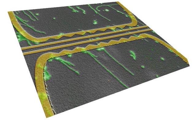
16 Organic Light-Emitting Diodes (OLEDs) OLED do not have a backlight unlike liquid crystal display (LCD). OLED create light by the following process: A battery or power supply sends a voltage through the OLED. An electrical current flows from the cathode to the organic layer and anode. As explained earlier, the anode removes electrons and adds electron holes in the conductive layer. Between the organic layers is where electrons fill the holes and give off energy in the form of photon light. 14
 Flexible Display Research")
17 Organic Light-Emitting Diodes (OLEDs) Flexible Display Research Trend 15

18 Flexible Display Applications 16
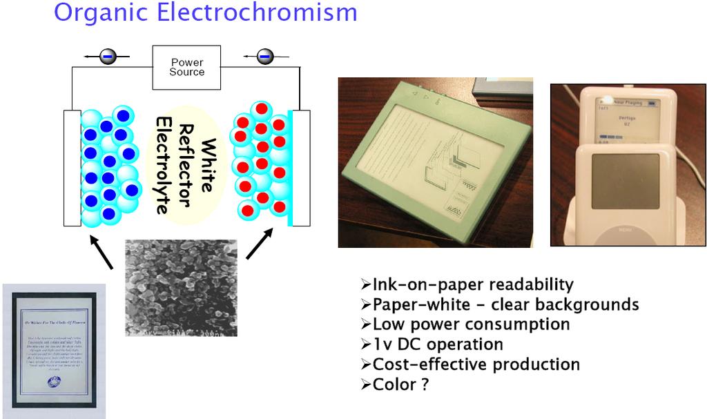
19 Electrochromic Display 20
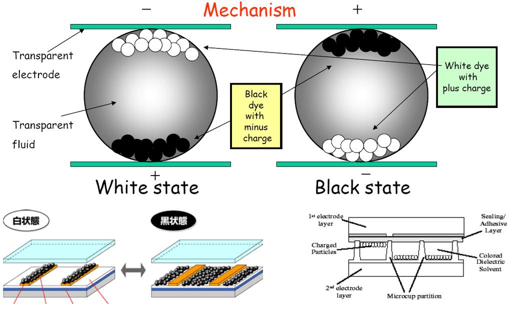
20 Electrophoretic Display 21

21 E-Ink Flexible Display 22
 0.")

22 Solar Cell Light energy (photons) Electrical energy Current (ma) P max I SC Voltage (V) V OC 32
23 The Solar Energy Resource Radiant power at Earth s surface~ TW Electricity consumption ~2 TW ~ 80% from fossil fuels & nuclear, ~0.05% from PV At 10% power conversion efficiency, solar resource can meet de mand with 0.02% of Earth surface area PV is the only technology to convert solar power directly into electricity PV Market Growth Present PV system costs: 7-20 Euro/W p off-grid applications. 4-8 Euro/W p grid-connected. Module 2 4 Euro / W p Aim for: 1-2 Euro/W p for power generation 4-10 Euro/W p for smaller applications. Cost of Si based system falling through economies of scale To accelerate cost reductions, need technological innovations 3.7 GW installed by end

24 Photovoltaic Efficiencies Compared 34


25 Strategies to Cost Reduction Strategies to cost reduction Use less photovoltaic material? Concentration of sunlight Light trapping More work per photon? Multijunction or tandem structures Extracting more work per photon Use cheaper photovoltaic materials and fabrication process? Organic thin film materials Printing Technology Molecular PV materials 35 35
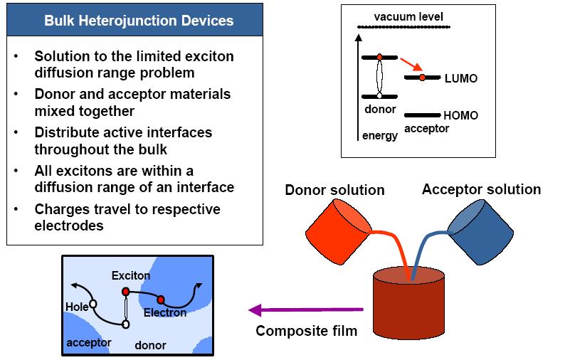
26 Bulk Heterojunction OPVs C 60 CP 36
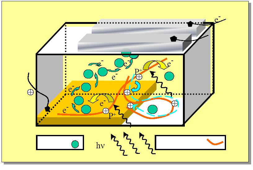
27 Operation Principle of Fullerene Organic Photovoltaics 37

28 Organic Photovoltaics (OPVs) OPV benefits from the opportunities of renewable energies but offers distinct competitive advantages Pros & Cons of Photovoltaics 38
 : Applications")
29 Organic Photovoltaics (OPVs) : Applications 39
 Source: Cristophe Brabec Konarka")
30 Module Stack for Organic Photovoltaics (OPVs) Source: Cristophe Brabec Konarka 40
31 Key Challenges for Organic Photovoltaics (OPVs) Current density J Organic solar cell Best h ~4-5% Voltage Electron acceptor Electron donor Maximum ev oc Silicon Best h 24% Irradiance /Wm -2 nm Wavelength / nm 41 41


32 Organic Thin-Film Transistors (OTFTs) Organic transistors are transistors that use organic molecules rather than silicon for their active material. This active material can be composed of a wide variety of molecules. P3HT Advantages compatibility with plastic substances lower temperature manufacturing ( C) lower-cost deposition processes such as spincoating, printing, evaporation less need to worry about dangling bonds makes for simpler processing Disadvantages lower mobility and switching speeds compared to silicon wafers usually do not operate under inversion mode (more on this later) [ Organic FET ] 24
")
33 Organic Thin-Film Transistors (OTFTs) Applications 25
")
34 Organic Thin-Film Transistors (OTFTs) Applications 26

")


35 Printed RFID Tags RFID for Item Level Tagging Organic Thin-Film Transistor (OTFT) Basic Element of Organic Integrated Circuit Inverter P-Channel & N-Channel OTFTs Ring Oscillator 27
 O S O O S")

 3.")
36 Materials for OTFTs 1. Conductor (Electrodes) O S O O S O O O S + O S O O n S O n m Colloidal ink of Au Nanoparticles (NP) SO 3 - HSO 3 2. Semiconductor (Active Layers) 3. Insulator (Gate Dielectrics) 28
37 Organic Semiconductors for OTFTs Monocrystalline Polycrystalline Amorphous solids Small molecules (SMs) SMs, polymers polymers pbttt Reproducibility of properties Luminescent property Environmental stability Mechanical stability moderate very high, low very high low moderate high moderate high, moderate high very low low, moderate high Electrical properties (mobility) very good good, moderate moderate to poor 29
38 Organic Semiconductors for OTFTs p-channel μ = cm 2 /Vs n-channel μ = 1-5 cm 2 /Vs cm 2 V -1 S -1 μ = cm 2 /Vs μ = cm 2 /Vs ~ 6 cm 2 V -1 S -1 (in Vacuum) μ = 0.01 cm 2 /Vs μ = 0.6 cm 2 /Vs cm 2 V -1 S -1 (1998, Vacuum Deposition) Relatively low field-effect mobility and air stability compared to p-channel materials μ = 0.1 cm 2 /Vs Significant progress in performance / reliability in recent years, but mobility still limited to cm 2 /Vs. 30

39 Progress in OTFTs Organic semiconductors come in 2 flavors Printed transistor 31
40 Organic Memory : Advantages and Applications Advantages Large area fabrication with extremely low cost Light-weight and flexibility High capacity with bottom-up stacking Capable ubiquitous components that are printed onto plastic, glass or metal foils Technology Performance Evaluation (Polymer Memory) Applications : Inexpensive data storage media : Disposable, mobile, flexible and low-duty applications. Ex.) RFID tag, smart card, e-paper, OLED driving circuit, etc. ITRS 2005 Emerging Research Devices 42


41 Organic Memory: Research Approaches OFET-Type Memory - Ferroelectric polymer insulator - Polarizable gate dielectrics Electrical Bistable Device - Electrical Biatability of Organic Semiconductor layer or Metal Nano-particles, etc. Hybrid Memory - In Combination of Inorganic and Organic Materials AIDCN (2-amino-4, 5- imidazoledicarbonitrile) [R.C.G. Naber, Nature Mater., 2005, 4, 243.] [Y. Yang, Appl. Phys. Lett. 2002, 80, 2997.] [S. Möller, Nature, 2003, 426, 13.] 43

42 Organic Materials to Nanotechnology : Scale without size

 perpendicular to c-axis parallel to")

43 Organic Materials to Nanotechnology : Graphene Graphite Conductivity: Electrical Resistivity (ohm.m) perpendicular to c-axis parallel to c-axis natural 9.8x x x10-6 Chris Ewels ( Single-layer graphene transistor 45

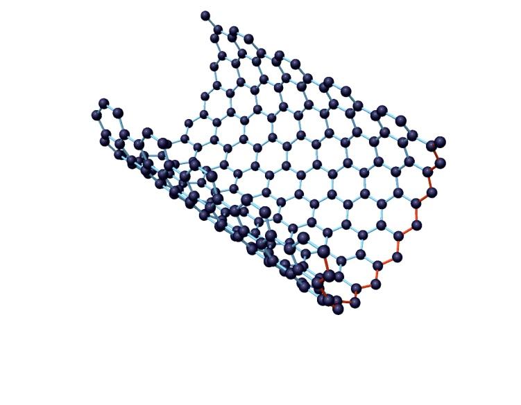

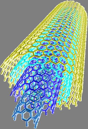
44 Organic Materials to Nanotechnology : Cabon Nanotube Roll-up of Graphite mesh nanotubes.html 46
Semiconductor Polymer
 Semiconductor Polymer Organic Semiconductor for Flexible Electronics Introduction: An organic semiconductor is an organic compound that possesses similar properties to inorganic semiconductors with hole
Molecular Electronics For Fun and Profit(?)
") Molecular Electronics For Fun and Profit(?) Prof. Geoffrey Hutchison Department of Chemistry University of Pittsburgh geoffh@pitt.edu July 22, 2009 http://hutchison.chem.pitt.edu Moore s Law: Transistor
Molecular Electronics For Fun and Profit(?) Prof. Geoffrey Hutchison Department of Chemistry University of Pittsburgh geoffh@pitt.edu July 22, 2009 http://hutchison.chem.pitt.edu Moore s Law: Transistor
Challenges in to-electric Energy Conversion: an Introduction
 Challenges in Solar-to to-electric Energy Conversion: an Introduction Eray S. Aydil Chemical Engineering and Materials Science Department Acknowledgements: National Science Foundation Minnesota Initiative
Organic Electronic Devices
 Organic Electronic Devices Week 5: Organic Light-Emitting Devices and Emerging Technologies Lecture 5.5: Course Review and Summary Bryan W. Boudouris Chemical Engineering Purdue University 1 Understanding
Halbleiter Prof. Yong Lei Prof. Thomas Hannappel
 Halbleiter Prof. Yong Lei Prof. Thomas Hannappel yong.lei@tu-ilmenau.de thomas.hannappel@tu-ilmenau.de http://www.tu-ilmenau.de/nanostruk/ Organic Semiconductors & Organic Electronics Organic semiconductors
Mesoporous titanium dioxide electrolyte bulk heterojunction
 Mesoporous titanium dioxide electrolyte bulk heterojunction The term "bulk heterojunction" is used to describe a heterojunction composed of two different materials acting as electron- and a hole- transporters,
Flexible Organic Photovoltaics Employ laser produced metal nanoparticles into the absorption layer 1. An Introduction
 Flexible Organic Photovoltaics Employ laser produced metal nanoparticles into the absorption layer 1. An Introduction Among the renewable energy sources that are called to satisfy the continuously increased
Plastic Electronics. Joaquim Puigdollers.
 Plastic Electronics Joaquim Puigdollers Joaquim.puigdollers@upc.edu Nobel Prize Chemistry 2000 Origins Technological Interest First products.. MONOCROMATIC PHILIPS Today Future Technological interest Low
Towards a deeper understanding of polymer solar cells
 Towards a deeper understanding of polymer solar cells Jan Anton Koster Valentin Mihailetchi Prof. Paul Blom Molecular Electronics Zernike Institute for Advanced Materials and DPI University of Groningen
Quantum Dots for Advanced Research and Devices
 Quantum Dots for Advanced Research and Devices spectral region from 450 to 630 nm Zero-D Perovskite Emit light at 520 nm ABOUT QUANTUM SOLUTIONS QUANTUM SOLUTIONS company is an expert in the synthesis
Development of active inks for organic photovoltaics: state-of-the-art and perspectives
 Development of active inks for organic photovoltaics: state-of-the-art and perspectives Jörg Ackermann Centre Interdisciplinaire de Nanoscience de Marseille (CINAM) CNRS - UPR 3118, MARSEILLE - France
High efficiency silicon and perovskite-silicon solar cells for electricity generation
 High efficiency silicon and perovskite-silicon solar cells for electricity generation Ali Dabirian Email: dabirian@ipm.ir 1 From Solar Energy to Electricity 2 Global accumulative PV installed In Iran it
Vikram Kuppa School of Energy, Environmental, Biological and Medical Engineering College of Engineering and Applied Science University of Cincinnati
 Vikram Kuppa School of Energy, Environmental, Biological and Medical Engineering College of Engineering and Applied Science University of Cincinnati vikram.kuppa@uc.edu Fei Yu Yan Jin Andrew Mulderig Greg
Photovoltaics. Lecture 7 Organic Thin Film Solar Cells Photonics - Spring 2017 dr inż. Aleksander Urbaniak
 Photovoltaics Lecture 7 Organic Thin Film Solar Cells Photonics - Spring 2017 dr inż. Aleksander Urbaniak Barcelona, Spain Perpignan train station, France source: pinterest Why organic solar cells? 1.
Chapter 12 - Modern Materials
 Chapter 12 - Modern Materials 12.1 Semiconductors Inorganic compounds that semiconduct tend to have chemical formulas related to Si and Ge valence electron count of four. Semiconductor conductivity can
Semiconductor Physics and Devices
 Syllabus Advanced Nano Materials Semiconductor Physics and Devices Textbook Donald A. Neamen (McGraw-Hill) Semiconductor Physics and Devices Seong Jun Kang Department of Advanced Materials Engineering
PHOTOVOLTAICS Fundamentals
 PHOTOVOLTAICS Fundamentals PV FUNDAMENTALS Semiconductor basics pn junction Solar cell operation Design of silicon solar cell SEMICONDUCTOR BASICS Allowed energy bands Valence and conduction band Fermi
Organic solar cells. State of the art and outlooks. Gilles Horowitz LPICM, UMR7647 CNRS - Ecole Polytechnique
 Organic solar cells. State of the art and outlooks Gilles Horowitz LPICM, UMR7647 CNRS - Ecole Polytechnique Solar energy Solar energy on earth: 75,000 tep/year 6000 times the world consumption in 2007
Physics of Organic Semiconductor Devices: Materials, Fundamentals, Technologies and Applications
 Physics of Organic Semiconductor Devices: Materials, Fundamentals, Technologies and Applications Dr. Alex Zakhidov Assistant Professor, Physics Department Core faculty at Materials Science, Engineering
Conjugated Polymers Based on Benzodithiophene for Organic Solar Cells. Wei You
 Wake Forest Nanotechnology Conference October 19, 2009 Conjugated Polymers Based on Benzodithiophene for Organic olar Cells Wei You Department of Chemistry and Institute for Advanced Materials, Nanoscience
Goal for next generation solar cells: Efficiencies greater than Si with low cost (low temperature) processing
 processing") Multi-junction cells MBE growth > 40% efficient Expensive Single crystal Si >20% efficient expensive Thin film cells >10% efficient Less expensive Toxic materials Polymers
Multi-junction cells MBE growth > 40% efficient Expensive Single crystal Si >20% efficient expensive Thin film cells >10% efficient Less expensive Toxic materials Polymers
GaN based transistors
 GaN based transistors S FP FP dielectric G SiO 2 Al x Ga 1-x N barrier i-gan Buffer i-sic D Transistors "The Transistor was probably the most important invention of the 20th Century The American Institute
Introduction. Fang-Chung Chen Department of Photonics and Display Institute National Chiao Tung University. Organic light-emitting diodes
 rganic light-emitting diodes Introduction Fang-Chung Chen Department of Photonics and Display Institute National Chiao Tung University rganic light-emitting diodes --The emerging technology LED Displays
Inorganic compounds that semiconduct tend to have an average of 4 valence electrons, and their conductivity may be increased by doping.
 Chapter 12 Modern Materials 12.1 Semiconductors Inorganic compounds that semiconduct tend to have an average of 4 valence electrons, and their conductivity may be increased by doping. Doping yields different
CHAPTER 11 Semiconductor Theory and Devices
 CHAPTER 11 Semiconductor Theory and Devices 11.1 Band Theory of Solids 11.2 Semiconductor Theory 11.3 Semiconductor Devices 11.4 Nanotechnology It is evident that many years of research by a great many
What will it take for organic solar cells to be competitive?
 What will it take for organic solar cells to be competitive? Michael D. McGehee Stanford University Director of the Center for Advanced Molecular Photovoltaics Efficiency (%) We will need 20-25 % efficiency
Introduction to Organic Solar Cells
 Introduction to Organic Solar Cells Dr Chris Fell Solar Group Leader CSIRO Energy Technology, Newcastle, Australia Organic semiconductors Conductivity in polyacetylene 1970s Nobel Prize Alan J. Heeger
Organic Electronic Devices
 Organic Electronic Devices Week 4: Organic Photovoltaic Devices Lecture 4.1: Overview of Organic Photovoltaic Devices Bryan W. Boudouris Chemical Engineering Purdue University 1 Lecture Overview and Learning
Basic Limitations to Third generation PV performance
 Basic Limitations to Third generation PV performance Pabitra K. Nayak Weizmann Institute of Science, Rehovot, Israel THANKS to my COLLEAGUES Lee Barnea and David Cahen. Weizmann Institute of Science Juan
GRAPHENE NANORIBBONS Nahid Shayesteh,
 USC Department of Physics Graduate Seminar 1 GRAPHENE NANORIBBONS Nahid Shayesteh, Outlines 2 Carbon based material Discovery and innovation of graphen Graphene nanoribbons structure Application of Graphene
Enhancing the Performance of Organic Thin-Film Transistor using a Buffer Layer
 Proceedings of the 9th International Conference on Properties and Applications of Dielectric Materials July 19-23, 29, Harbin, China L-7 Enhancing the Performance of Organic Thin-Film Transistor using
Planar Organic Photovoltaic Device. Saiful I. Khondaker
 Planar Organic Photovoltaic Device Saiful I. Khondaker Nanoscience Technology Center and Department of Physics University of Central Florida http://www.physics.ucf.edu/~khondaker W Metal 1 L ch Metal 2
Paper and Cellulosic Materials as Flexible Substrates for 2D Electronic Materials
 Paper and Cellulosic Materials as Flexible Substrates for 2D Electronic Materials Prof. Eric M. Vogel, Prof. M. Shofner, Brian Beatty Materials Science & Engineering Trends in Electronics Internet of things
Charge Extraction from Complex Morphologies in Bulk Heterojunctions. Michael L. Chabinyc Materials Department University of California, Santa Barbara
 Charge Extraction from Complex Morphologies in Bulk Heterojunctions Michael L. Chabinyc Materials Department University of California, Santa Barbara OPVs Vs. Inorganic Thin Film Solar Cells Alta Devices
Introducing the RoVaCBE Flagship project: Roll-to-roll Vacuum-processed Carbon Based Electronics. Dr Hazel Assender, University of Oxford
 Introducing the RoVaCBE Flagship project: Roll-to-roll Vacuum-processed Carbon Based Electronics Dr Hazel Assender, University of Oxford DALMATIAN TECHNOLOGY 21 st Sept 2010 1 Organic electronics Opportunity
Nanoelectronics. Topics
 Nanoelectronics Topics Moore s Law Inorganic nanoelectronic devices Resonant tunneling Quantum dots Single electron transistors Motivation for molecular electronics The review article Overview of Nanoelectronic
Carbon Nanomaterials: Nanotubes and Nanobuds and Graphene towards new products 2030
 Carbon Nanomaterials: Nanotubes and Nanobuds and Graphene towards new products 2030 Prof. Dr. Esko I. Kauppinen Helsinki University of Technology (TKK) Espoo, Finland Forecast Seminar February 13, 2009
Session V: Graphene. Matteo Bruna CAMBRIDGE UNIVERSITY DEPARTMENT OF ENGINEERING
 Session V: Graphene Matteo Bruna Graphene: Material in the Flatland Graphite Graphene Properties: Thinnest imaginable material Good(and tunable) electrical conductor Strongest ever measured Stiffest known
Self Assembled Monolayers
 Nanotechnology for engineers Winter semester 2005-2006 Plastic Electronics - Self Assembled Monolayers - Organic Materials Based Devices - Organic photovoltaic devices Nanotechnology for engineers Winter
TECHNICAL INFORMATION. Quantum Dot
 Quantum Dot Quantum Dot is the nano meter sized semiconductor crystal with specific optical properties originates from the phenomenon which can be explained by the quantum chemistry and quantum mechanics.
Real-time and in-line Optical monitoring of Functional Nano-Layer Deposition on Flexible Polymeric Substrates
 Real-time and in-line Optical monitoring of Functional Nano-Layer Deposition on Flexible Polymeric Substrates S. Logothetidis Lab for Thin Films, Nanosystems & Nanometrology, Aristotle University of Thessaloniki,
PV Tutorial Allen Hermann, Ph. D. Professor of Physics Emeritus, and Professor of Music Adjunct, University of Colorado, Boulder, Colorado, USA and
 PV Tutorial Allen Hermann, Ph. D. Professor of Physics Emeritus, and Professor of Music Adjunct, University of Colorado, Boulder, Colorado, USA and Vice-president, NanoTech Inc. Lexington, Kentucky, USA
Nanomaterials & Organic Electronics Group TEI of Crete
 Nanomaterials & Organic Electronics Group TEI of Crete Dr. Emmanuel Kymakis Asc. Professor, Dept. of Electrical Engineering and Center of Advanced Materials & Photonics kymakis@staff.teicrete.gr http://nano.teicrete.gr/
NANO TECHNOLOGY IN POLYMER SOLAR CELLS. Mayur Padharia, Hardik Panchal, Keval Shah, *Neha Patni, Shibu.G.Pillai
 NANO TECHNOLOGY IN POLYMER SOLAR CELLS Mayur Padharia, Hardik Panchal, Keval Shah, *Neha Patni, Shibu.G.Pillai Department of Chemical Engineering, Institute of Technology, Nirma University, S. G. Highway,
EE130: Integrated Circuit Devices
 EE130: Integrated Circuit Devices (online at http://webcast.berkeley.edu) Instructor: Prof. Tsu-Jae King (tking@eecs.berkeley.edu) TA s: Marie Eyoum (meyoum@eecs.berkeley.edu) Alvaro Padilla (apadilla@eecs.berkeley.edu)
University of Groningen. Molecular Solar Cells Hummelen, Jan. Published in: EPRINTS-BOOK-TITLE
 University of Groningen Molecular Solar Cells Hummelen, Jan Published in: EPRINTS-BOOK-TITLE IMPORTANT NOTE: You are advised to consult the publisher's version (publisher's PDF) if you wish to cite from
Enhanced Optical and Electrical Properties of Organic Field Effect Transistor using Metal Nanoparticles
 University of Miami Scholarly Repository Open Access Theses Electronic Theses and Dissertations 2014-07-28 Enhanced Optical and Electrical Properties of Organic Field Effect Transistor using Metal Nanoparticles
Introduction to Photovoltaics
 INTRODUCTION Objectives Understand the photovoltaic effect. Understand the properties of light. Describe frequency and wavelength. Understand the factors that determine available light energy. Use software
Photoconductive Atomic Force Microscopy for Understanding Nanostructures and Device Physics of Organic Solar Cells
 Photoconductive AFM of Organic Solar Cells APP NOTE 15 Photoconductive Atomic Force Microscopy for Understanding Nanostructures and Device Physics of Organic Solar Cells Xuan-Dung Dang and Thuc-Quyen Nguyen
SEMINAR. Organic Semiconductor Thin Film Transistors
 University of Ljubljana Faculty of Mathematics and Physics Department of Physics SEMINAR Organic Semiconductor Thin Film Transistors Author: Tomaž Mlakar Adviser: Dr. Gvido Bratina Nova Gorica Polytechnic
Solids. Solids are everywhere. Looking around, we see solids. Composite materials make airplanes and cars lighter, golf clubs more powerful,
 Solids Solids are everywhere. Looking around, we see solids. Most of our electronics is solid state. Composite materials make airplanes and cars lighter, golf clubs more powerful, In addition to hard matter
Transparent Electrode Applications
 Transparent Electrode Applications LCD Solar Cells Touch Screen Indium Tin Oxide (ITO) Zinc Oxide (ZnO) - High conductivity - High transparency - Resistant to environmental effects - Rare material (Indium)
Perovskite quantum dots: a new absorber technology with unique phase stability for high voltage solar cells
 Perovskite quantum dots: a new absorber technology with unique phase stability for high voltage solar cells Joseph M. Luther National Renewable Energy Laboratory, Golden, CO NREL PV Systems: South Table
Classification of Solids
 Classification of Solids Classification by conductivity, which is related to the band structure: (Filled bands are shown dark; D(E) = Density of states) Class Electron Density Density of States D(E) Examples
Opto-electronic Characterization of Perovskite Thin Films & Solar Cells
 Opto-electronic Characterization of Perovskite Thin Films & Solar Cells Arman Mahboubi Soufiani Supervisors: Prof. Martin Green Prof. Gavin Conibeer Dr. Anita Ho-Baillie Dr. Murad Tayebjee 22 nd June 2017
Published in: ELECTRONIC PROPERTIES OF NOVEL MATERIALS - PROGRESS IN MOLECULAR NANOSTRUCTURES
 University of Groningen Fullerenes and nanostructured plastic solar cells Knol, Joop; Hummelen, Jan Published in: ELECTRONIC PROPERTIES OF NOVEL MATERIALS - PROGRESS IN MOLECULAR NANOSTRUCTURES IMPORTANT
Supplementary Information. Effect of thermal annealing Super Yellow emissive layer on efficiency of OLEDs
 Supplementary Information Effect of thermal annealing Super Yellow emissive layer on efficiency of OLEDs Samantha Burns 1, Jennifer MacLeod 1,2, Thu Trang Do 1, Prashant Sonar 1, Soniya D. Yambem 1,3,*
Observation of electron injection in an organic field-effect transistor with electroluminescence *
 Materials Science-Poland, Vol. 27, No. 3, 2009 Observation of electron injection in an organic field-effect transistor with electroluminescence * Y. OHSHIMA **, H. KOHN, E. LIM, T. MANAKA, M. IWAMOTO Department
Electrons are shared in covalent bonds between atoms of Si. A bound electron has the lowest energy state.
 Photovoltaics Basic Steps the generation of light-generated carriers; the collection of the light-generated carriers to generate a current; the generation of a large voltage across the solar cell; and
EE 446/646 Photovoltaic Devices I. Y. Baghzouz
 EE 446/646 Photovoltaic Devices I Y. Baghzouz What is Photovoltaics? First used in about 1890, the word has two parts: photo, derived from the Greek word for light, volt, relating to electricity pioneer
Structure Property Relationships of. Organic Light-Emitting Diodes. Michael Kochanek May 19, 2006 MS&E 542 Flexible Electronics
 Structure Property Relationships of Organic Light-Emitting Diodes Michael Kochanek May 19, 2006 MS&E 542 Flexible Electronics Introduction Many of today s solid-state inorganic microelectronic devices
Unit 02 Modules Systems. Components. Marcus Rennhofer : Modules, Systems & Components
 Unit 02 Modules Systems Marcus Rennhofer marcus.rennhofer@ait.ac.at Content: Systems & System System types Module & Inverter Solar batteries Electric circuit Technology Families Crystalline solar cells
e - Galvanic Cell 1. Voltage Sources 1.1 Polymer Electrolyte Membrane (PEM) Fuel Cell
 Fuel Cell") Galvanic cells convert different forms of energy (chemical fuel, sunlight, mechanical pressure, etc.) into electrical energy and heat. In this lecture, we are interested in some examples of galvanic cells.
Galvanic cells convert different forms of energy (chemical fuel, sunlight, mechanical pressure, etc.) into electrical energy and heat. In this lecture, we are interested in some examples of galvanic cells.
Nanostrukturphysik (Nanostructure Physics)
") Nanostrukturphysik (Nanostructure Physics) Prof. Yong Lei & Dr. Yang Xu Fachgebiet 3D-Nanostrukturierung, Institut für Physik Contact: yong.lei@tu-ilmenau.de; yang.xu@tu-ilmenau.de Office: Unterpoerlitzer
Nanostrukturphysik (Nanostructure Physics) Prof. Yong Lei & Dr. Yang Xu Fachgebiet 3D-Nanostrukturierung, Institut für Physik Contact: yong.lei@tu-ilmenau.de; yang.xu@tu-ilmenau.de Office: Unterpoerlitzer
Synthesis Breakout. Overarching Issues
 Synthesis Breakout. Overarching Issues 1. What are fundamental structural and electronic factors limiting Jsc, Voc, and FF in typical polymer bulk-heterojunction cells? Rational P- and N-type materials
LECTURE 23. MOS transistor. 1 We need a smart switch, i.e., an electronically controlled switch. Lecture Digital Circuits, Logic
 LECTURE 23 Lecture 16-20 Digital Circuits, Logic 1 We need a smart switch, i.e., an electronically controlled switch 2 We need a gain element for example, to make comparators. The device of our dreams
Time Scaling with System Size for Resistor-Only Warm Up for Photovoltaic Device Simulation
 Time Scaling with System Size for Resistor-Only Warm Up for Photovoltaic Device Simulation Ashley Gazich Department of Mathematics, University of Florida, Gainesville, FL Advised by Dr. Selman Hershfield
ELECTRONIC DEVICES AND CIRCUITS SUMMARY
 ELECTRONIC DEVICES AND CIRCUITS SUMMARY Classification of Materials: Insulator: An insulator is a material that offers a very low level (or negligible) of conductivity when voltage is applied. Eg: Paper,
Chapter 12. Modern Materials. Chapter 12 Problems 7/3/2012. Problems 1, 4, 7, 9, 11, 13, 23, 29, 3143, 53, 55
 hemistry, The entral Science, 11th edition Theodore L. Brown, H. Eugene LeMay, Jr., and Bruce E. Bursten hapter 12 John D. Bookstaver St. harles ommunity ollege ottleville, MO hapter 12 Problems Problems
TABLE OF CONTENTS 1 RESEARCH SCOPE AND METHODOLOGY Report scope Market definition Categorization...
 TABLE OF CONTENTS 1 RESEARCH SCOPE AND METHODOLOGY... 15 1.1 Report scope... 15 1.2 Market definition... 15 1.2.1 Categorization.... 16 1.3 Research methodology... 17 1.4 Assumptions and limitations...
Organic Field-Effect Transistors - Introduction -
 Organic Field-Effect Transistors - Introduction - 1. Introduction to OFETs Field-Effect Transistor? Transistor A device composed of semiconductor material that amplifies a signal or opens or closes a circuit.
Nanostructural properties 2009/10 Mini-course on fundamental electronic and optical properties of organic semiconductors (part 1) Lorenzo Stella
 Lorenzo Stella") Nanostructural properties 2009/10 Mini-course on fundamental electronic and optical properties of organic semiconductors (part 1) Lorenzo Stella Nano-bio group - ETSF lorenzo.stella@ehu.es Outline A. Introduction
Nanostructural properties 2009/10 Mini-course on fundamental electronic and optical properties of organic semiconductors (part 1) Lorenzo Stella Nano-bio group - ETSF lorenzo.stella@ehu.es Outline A. Introduction
From nanophysics research labs to cell phones. Dr. András Halbritter Department of Physics associate professor
 From nanophysics research labs to cell phones Dr. András Halbritter Department of Physics associate professor Curriculum Vitae Birth: 1976. High-school graduation: 1994. Master degree: 1999. PhD: 2003.
EN2912C: Future Directions in Computing Lecture 08: Overview of Near-Term Emerging Computing Technologies
 EN2912C: Future Directions in Computing Lecture 08: Overview of Near-Term Emerging Computing Technologies Prof. Sherief Reda Division of Engineering Brown University Fall 2008 1 Near-term emerging computing
Wafer-scale fabrication of graphene
 Wafer-scale fabrication of graphene Sten Vollebregt, MSc Delft University of Technology, Delft Institute of Mircosystems and Nanotechnology Delft University of Technology Challenge the future Delft University
Organic devices and electronics -for non-display application
 Chalmers 2006-05-17 Examiner: Thorvald Andersson Miniproject in FMI040 Semiconductor Materials Physics Organic devices and electronics -for non-display application Tutor: Måns Andreasson Group members:
Appendix A. MS713M: Organic Materials. New Course Code and Title Course Coordinator. AP Andrew Grimsdale. Rationale for introducing this course
 New Course Code and Title Course Coordinator Details of Course MS713M: Organic Materials AP Andrew Grimsdale Rationale for introducing this course This course will cover the subject of organic materials.
Photovoltaic cell and module physics and technology
 Photovoltaic cell and module physics and technology Vitezslav Benda, Prof Czech Technical University in Prague benda@fel.cvut.cz www.fel.cvut.cz 6/21/2012 1 Outlines Photovoltaic Effect Photovoltaic cell
Organic Solar Cells. All Organic solar cell. Dye-sensitized solar cell. Dye. τ inj. τ c. τ r surface states D*/D + V o I 3 D/D.
 The 4th U.S.-Korea NanoForum April 26-27, 2007, Honolulu, USA Improvement of Device Efficiency in Conjugated Polymer/Fullerene NanoComposite Solar Cells School of Semiconductor & Chemical Engineering *
3.1 Introduction to Semiconductors. Y. Baghzouz ECE Department UNLV
 3.1 Introduction to Semiconductors Y. Baghzouz ECE Department UNLV Introduction In this lecture, we will cover the basic aspects of semiconductor materials, and the physical mechanisms which are at the
Designing Information Devices and Systems II A. Sahai, J. Roychowdhury, K. Pister Discussion 1A
 EECS 16B Spring 2019 Designing Information Devices and Systems II A. Sahai, J. Roychowdhury, K. Pister Discussion 1A 1 Semiconductor Physics Generally, semiconductors are crystalline solids bonded into
Semiconductors and Optoelectronics. Today Semiconductors Acoustics. Tomorrow Come to CH325 Exercises Tours
 Semiconductors and Optoelectronics Advanced Physics Lab, PHYS 3600 Don Heiman, Northeastern University, 2017 Today Semiconductors Acoustics Tomorrow Come to CH325 Exercises Tours Semiconductors and Optoelectronics
UNIVERSITY OF CALIFORNIA College of Engineering Department of Electrical Engineering and Computer Sciences. Fall Exam 1
 UNIVERSITY OF CALIFORNIA College of Engineering Department of Electrical Engineering and Computer Sciences EECS 143 Fall 2008 Exam 1 Professor Ali Javey Answer Key Name: SID: 1337 Closed book. One sheet
MSE 310/ECE 340: Electrical Properties of Materials Fall 2014 Department of Materials Science and Engineering Boise State University
 MSE 310/ECE 340: Electrical Properties of Materials Fall 2014 Department of Materials Science and Engineering Boise State University Practice Final Exam 1 Read the questions carefully Label all figures
EE236 Electronics. Computer and Systems Engineering Department. Faculty of Engineering Alexandria University. Fall 2014
 EE236 Electronics Computer and Systems Engineering Department Faculty of Engineering Alexandria University Fall 2014 Lecturer: Bassem Mokhtar, Ph.D. Assistant Professor Department of Electrical Engineering
Forming Gradient Multilayer (GML) Nano Films for Photovoltaic and Energy Storage Applications
 Nano Films for Photovoltaic and Energy Storage Applications") Forming Gradient Multilayer (GML) Nano Films for Photovoltaic and Energy Storage Applications ABSTRACT Boris Gilman and Igor Altman Coolsol R&C, Mountain View CA For successful implementation of the nanomaterial-based
Forming Gradient Multilayer (GML) Nano Films for Photovoltaic and Energy Storage Applications ABSTRACT Boris Gilman and Igor Altman Coolsol R&C, Mountain View CA For successful implementation of the nanomaterial-based
2008 Solar Annual Review Meeting
 2008 Solar Annual Review Meeting Session: Organic Photovoltaics Company: Konarka Funding Opportunity: $3.6M (DOE) $8.7M (total) Jeremiah Mwaura (jmwaura@konarka.com) Presenter s Name, Contact Information
Chapter 3 Basics Semiconductor Devices and Processing
 Chapter 3 Basics Semiconductor Devices and Processing Hong Xiao, Ph. D. www2.austin.cc.tx.us/hongxiao/book.htm Hong Xiao, Ph. D. www2.austin.cc.tx.us/hongxiao/book.htm 1 Objectives Identify at least two
Sandra Plaza García. Departamento de Física de Materiales, Facultad de Ciencias Químicas, Universidad del País Vasco (UPV)
") DOPING AND CONDUCTING POLYMERS Sandra Plaza García Departamento de Física de Materiales, Facultad de Ciencias Químicas, Universidad del País Vasco (UPV) Donostia International Physics Center (DIPC) OUTLINE
DOPING AND CONDUCTING POLYMERS Sandra Plaza García Departamento de Física de Materiales, Facultad de Ciencias Químicas, Universidad del País Vasco (UPV) Donostia International Physics Center (DIPC) OUTLINE
2D MBE Activities in Sheffield. I. Farrer, J. Heffernan Electronic and Electrical Engineering The University of Sheffield
 2D MBE Activities in Sheffield I. Farrer, J. Heffernan Electronic and Electrical Engineering The University of Sheffield Outline Motivation Van der Waals crystals The Transition Metal Di-Chalcogenides
ESE370: Circuit-Level Modeling, Design, and Optimization for Digital Systems
 ESE370: Circuit-Level Modeling, Design, and Optimization for Digital Systems Lec 6: September 14, 2015 MOS Model You are Here: Transistor Edition! Previously: simple models (0 and 1 st order) " Comfortable
2.626 Fundamentals of Photovoltaics
 MIT OpenCourseWare http://ocw.mit.edu 2.626 Fundamentals of Photovoltaics Fall 2008 For information about citing these materials or our Terms of Use, visit: http://ocw.mit.edu/terms. Charge Separation:
Seminars in Nanosystems - I
 Seminars in Nanosystems - I Winter Semester 2011/2012 Dr. Emanuela Margapoti Emanuela.Margapoti@wsi.tum.de Dr. Gregor Koblmüller Gregor.Koblmueller@wsi.tum.de Seminar Room at ZNN 1 floor Topics of the
Lecture 0: Introduction
 Lecture 0: Introduction Introduction q Integrated circuits: many transistors on one chip q Very Large Scale Integration (VLSI): bucketloads! q Complementary Metal Oxide Semiconductor Fast, cheap, low power
3/10/2013. Lecture #1. How small is Nano? (A movie) What is Nanotechnology? What is Nanoelectronics? What are Emerging Devices?
 What is Nanotechnology? What is Nanoelectronics? What are Emerging Devices?") EECS 498/598: Nanocircuits and Nanoarchitectures Lecture 1: Introduction to Nanotelectronic Devices (Sept. 5) Lectures 2: ITRS Nanoelectronics Road Map (Sept 7) Lecture 3: Nanodevices; Guest Lecture by
EECS 498/598: Nanocircuits and Nanoarchitectures Lecture 1: Introduction to Nanotelectronic Devices (Sept. 5) Lectures 2: ITRS Nanoelectronics Road Map (Sept 7) Lecture 3: Nanodevices; Guest Lecture by
Organic solar cells with inverted layer sequence incorporating optical spacers - simulation and experiment.
 Organic solar cells with inverted layer sequence incorporating optical spacers - simulation and experiment. Birger Zimmermann a, Markus Glatthaar a, Michael Niggemann Author3 a,b, Moritz Kilian Riede b,
Photovoltaic Energy Conversion. Frank Zimmermann
 Photovoltaic Energy Conversion Frank Zimmermann Solar Electricity Generation Consumes no fuel No pollution No greenhouse gases No moving parts, little or no maintenance Sunlight is plentiful & inexhaustible
CME 300 Properties of Materials. ANSWERS: Homework 9 November 26, As atoms approach each other in the solid state the quantized energy states:
 CME 300 Properties of Materials ANSWERS: Homework 9 November 26, 2011 As atoms approach each other in the solid state the quantized energy states: are split. This splitting is associated with the wave
Lecture 1. OUTLINE Basic Semiconductor Physics. Reading: Chapter 2.1. Semiconductors Intrinsic (undoped) silicon Doping Carrier concentrations
 silicon Doping Carrier concentrations") Lecture 1 OUTLINE Basic Semiconductor Physics Semiconductors Intrinsic (undoped) silicon Doping Carrier concentrations Reading: Chapter 2.1 EE105 Fall 2007 Lecture 1, Slide 1 What is a Semiconductor? Low
Lecture 1 OUTLINE Basic Semiconductor Physics Semiconductors Intrinsic (undoped) silicon Doping Carrier concentrations Reading: Chapter 2.1 EE105 Fall 2007 Lecture 1, Slide 1 What is a Semiconductor? Low
Chap. 1 (Introduction), Chap. 2 (Components and Circuits)
, Chap. 2 (Components and Circuits)") CHEM 455 The class describes the principles and applications of modern analytical instruments. Emphasis is placed upon the theoretical basis of each type of instrument, its optimal area of application,
CHEM 455 The class describes the principles and applications of modern analytical instruments. Emphasis is placed upon the theoretical basis of each type of instrument, its optimal area of application,