Organic Field-Effect Transistors - Introduction -
|
|
|
- Ginger Dorsey
- 6 years ago
- Views:
Transcription

1 Organic Field-Effect Transistors - Introduction -


2 1. Introduction to OFETs Field-Effect Transistor? Transistor A device composed of semiconductor material that amplifies a signal or opens or closes a circuit. The key ingredient of all digital circuits, including computers. Today's microprocessors contains tens of millions of microscopic c transistors. Field-Effect Transistor (FET) A voltage applied between the gate and source controls the current flowing between the source and drain.

3 1. Introduction to OFETs Field-Effect Transistor? - FET works like a dam! Gate Source Source Drain Base Gate Drain

4 1. Introduction to OFETs Organic Field-Effect Transistor (OFET) Organic transistors are transistors that use organic molecules rather than silicon for their active material. This active material can be composed of a wide variety of molecules. OFETs Advantages compatibility with plastic substances lower temperature manufacturing ( C) lower-cost deposition processes such as spincoating, printing, evaporation less need to worry about dangling bonds makes for simpler processing [ I-V Characteristics] [ Pentacene] Disadvantages lower mobility and switching speeds compared to silicon wafers usually do not operate under inversion mode (more on this later) [ Device Configuration ]

5 1. Introduction to OFETs Applications of OFETs
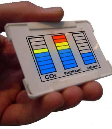
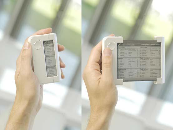
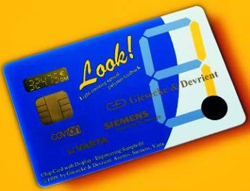
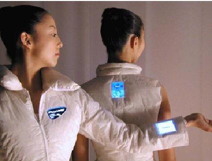
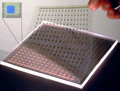
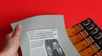
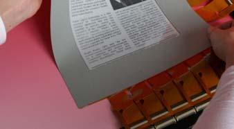
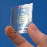
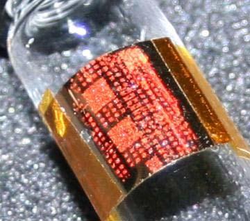
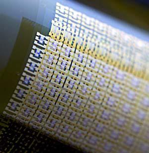
6 1. Introduction to OFETs Applications of OFETs [ Lab on a Chip ] [ Portable Screen ] [ Smart Textile ] Organic Transistor [ RFID tag ] [ Smart Card ] [ e-paper ] [ Flexible Circuits ]
7 2. Operation Mechanism of OFETs Metal-Oxide-Semiconductor FET (MOSFET) - OFET is based on Si-based MOSFET technology in its fundamental principle, application, and operating mechanism. Principle of MOSFET qφ M =4.1eV qχ ox =0.95eV Ec qχ Si =4.05eV Vacuum level qφ S =4.9eV 0.4eV 3.15eV 3.1eV E g 9eV Al E V Silicon 4.6eV SiO 2 V s = 0 V V g >0 V V d >0 V I d Ideal switch I on n + Channel n + Depletion p-type MOSFET I off V th V g

8 2. Operation Mechanism of OFETs Device Configuration of OFETs Each of these devices has particular advantages and disadvantages in the fabrication process, which will be discussed.
9 2. Operation Mechanism of OFETs Basic Operation Mechanism of OFETs V S = 0 V Organic Semiconductor Source Drain Insulator V D Gate V G
10 2. Operation Mechanism of OFETs Basic Operation Mechanism of OFETs
11 2. Operation Mechanism of OFETs Current-Voltage (I-V) Characteristics Output (I d -V d ) Curve W C = μ L V 2 i d I d, lin ( Vg VTh ) -100 V d Linear region Saturation region I W C = μ 2L i 2 d, Sat ( Vg VTh) I d [μα] V g = -50 V V g = -40 V V g = -30 V V g > V Th V d [V] V g < V Th
12 2. Operation Mechanism of OFETs Current-Voltage (I-V) Characteristics Transfer (I d -V g ) Curve Performance Parameters At saturation region -I d 1/2 [A 1/2 ] I on 1.2x10⁻² V d = -30 V 1.0x x x x10-3 Slope SS 2.0x V g [V] I d [A] I off I W C = μ 2L i 2 d, Sat ( Vg VTh) 1. Field-Effect Mobility (μ) [cm 2 /Vs] μ = SS 2L WC i [ V = [log ( Slope) 2. Sub-threshold Swing (SS) [V/dec.] g ] I 10 d 3. On/Off Ratio (I On/ /I off ) ] 2 4. Threshold Voltage (V Th ) [V] V Th V on
 Low Threshold Voltage (V Th ) Steep Sub-threshold")
13 3. Important Factors to Get High Performance OFETs Important Factors Requirements for high performance OFETs High Mobility High On/off Ratio (I on /I off ) Low Threshold Voltage (V Th ) Steep Sub-threshold Slope
 : Conjugated polymers (ex. P3HT, F8T2) Inorganic S.C. (ex. a-si:h, zinc oxide) Insulator layer Organic Dielectrics (ex.")
14 3. Important Factors to Get High Performance OFETs Materials for OFETs Semiconductor layer V G C A : semiconductor B: metal electrode (Au, Ag) C: gate Key Characteristics High Mobility High I on/off Low Threshold Voltage Organic S.C.: : Small molecules (ex. pentacene, oligothiophene) : Conjugated polymers (ex. P3HT, F8T2) Inorganic S.C. (ex. a-si:h, zinc oxide) Insulator layer Organic Dielectrics (ex. PVP, PMMA, BCB, Polyimide) Inorganic Dielectrics (ex. SiO 2, Al 2 O 3, TiO 2 ) Electrodes Metal (ex. Au, Ca) Conducting Polymer (ex. PEDOT:PSS)
15 3. Important Factors to Get High Performance OFETs Requirements of Materials for OFETs
16 3. Important Factors to Get High Performance OFETs Factors influencing OFET Performance Performance Parameter On-Current Off-Current Mobility Sub-threshold slope Dominant Factor W/L Mobility Interface states Contact resistance Gap states W/L Fermi level Interface states Contact resistance Band gap Gate insulator Grain boundary Interface states Gap states Interface states

17 3-1. Organic Semiconductor Charge Transport in Organic Semiconductors Molecular Orbitals of the Ethene Molecule r/a antibonding molecular π atomic p z atomic p z r/a molecular π bonding
18 3-1. Organic Semiconductor Charge Transport in Organic Semiconductors
19 3-1. Organic Semiconductor Charge Transport in Organic Semiconductors Organic polymers Organic and molecular crystals Inorganic materials TMTSF 2 PF 6 (superconducting) Cu Conductivity (S cm 1 ) Graphite Pyropolymers Polyacetylene Poly(p-phenylene) Poly(phenylene sulphide) Polypyrrole Polythiophene Polyphthalocyanine Polyacetylene (undoped) doped polymers TTF-TCNQ Cu-TCNQ Ag-TCNQ Hg Bi Si ZnO Ge (doped) Si Boron H 2 O Iodine metals semiconductors Polydiacetylene Polythiophene Polypyrrole (undoped) Nylon Poly(p-phenylene) (undoped) Poly (phenylene sulphide) (undoped) PVC Polystyrene Polyimide (Kapton) PTFE (Teflon) Cu-phthalocyanine Anthracene ZnO Diamond SiO 2 insulators
20 3-1. Organic Semiconductor Organic Semiconductors for OFETs P-type N-type

21 3-1. Organic Semiconductor Organic Semiconductors for OFETs
22 3-1. Organic Semiconductor Organic Semiconductors for OFETs

23 3-1. Organic Semiconductor Conduction Mechanism in OFET Channel Field-Effect Mobility of OFET is determined by intrinsic or extrinsic charge transport mechanism of the organic semiconductors

.")

24 3-1. Organic Semiconductor Conduction Mechanism in OFET Channel Charge Transport in Organic Single Crystal Upper limit of mobility in organic single crystal at room temperature is 1~10 cm 2 V -1 s -1 due to the weak intermolecular interaction forces (van der waals interaction) of 10kcal/mole (cf. 76kcal/mole for Si (convalent bond). F i : intermolecular interaction force F V : thermal vibration force Low Temperature High Temperature - Strong π-orbital overlap - Band transport - Negative temp. coefficient - Weak π-orbital overlap - Hopping transport - Positive temp. coefficient F i F V
25 3-1. Organic Semiconductor Conduction Mechanism in OFET Channel Charge Transport in Polymer Intra-molecular - Soliton propagation : μ= 1,000cm 2 /V.sec Inter-molecular - Hopping transport : μ= 10-3 cm 2 /V.sec» It is important to increase molecular ordering to obtain high field-effect mobility in OFET devices

 - Hopping-type charge carrier transport dominant - Low charge carrier")
 - Band-type charge carrier transport dominant - High carrier")
26 3-1. Organic Semiconductor Organic & Inorganic Semiconductors Organic Semiconductor Inorganic Semiconductor Weak Van der Waals interaction forces : π-bond overlapping - Slight change of electronic structure - Retaining molecule s identity - Between molecular gas and covalent crystal (Molecular property + crystal property) - Hopping-type charge carrier transport dominant - Low charge carrier mobility and small mean free path Strong covalent bonds :ρ bond - Complete loss of individual properties (Only crystal properties) - Band-type charge carrier transport dominant - High carrier mobility and large mean free path

27 3-1. Organic Semiconductor Bipolar OFETs OSC in Interfacial Properties Idealized energy level diagram of OFETs N-channel operation V G = 0 LUMO HOMO V D = 0 P-channel operation Ambipolar behavior of OFETs source drain V G > V D = 0 V G < V D = 0 Electron accumulation Hole accumulation V G > 0 V D > 0 V G < V D < 0 Protecting OH functional with BCB Electron transport Hole transport Friend et. al. Nature, 2005
28 3-1. Organic Semiconductor Extrinsic Effects on Charge Transport Charge Transport in Polycrystalline Semiconductors Mobilty (cm 2 V -1 s -1 ) E-3 1E-4 Band Grain boundary polaron hopping Far range hopping Transport mechanism Disorder
29 3-1. Organic Semiconductor Extrinsic Effects on Charge Transport Scattering Mechanism in Organic Thin-Film
30 3-1. Organic Semiconductor Extrinsic Effects on Charge Transport Free and Trapped Carriers Field-Effect Induced Carrier Density Gate E F + + Organic Semiconductor Traps Accumulation Layer E C E V p C i V g /e p = p f + p t Q = p f /(p f +p t ) m FET Q m o < m o Sample Dependence of m FET (Growth Conditions, Preparation ) Gate Voltage Dependence Degradation / Instabilities Insulator
31 3-1. Organic Semiconductor Extrinsic Effects on Charge Transport Traps in OFETs Insulator Interface Bulk E v Grain Boundary Source of trap: impurity, grain boundary, misfit etc. If the interface trap density (C it ) is high, the subthreshold slope (S) is increased kt Cdm + C S = q COx it

32 3-1. Organic Semiconductor Disorder and OFET Characteristics
33 3-2. Gate Insulators Requirements for OFET Dielectrics Requirements for OFET Dielectrics 1) High dielectric constant for low-voltage operating 2) Good heat and chemical resistance 3) Pinhole free thin film formability with high breakdown voltage and long term stability 4) Comparable with organic semiconductor in interfacial properties Low k CYMM Commonly used
34 3-2. Gate Insulators Potential Dielectric Effects in OFETs The conduction mechanism in organic semiconductors is different from that of inorganics. Due to the weak intermolecular forces in OSC, the number of effects through which the dielectric can influence carrier transport and mobility is much broader than n in inorganic materials. Dielectric Effects in OFETs Morphology of organic semiconductor and orientation of molecular segments via their interaction with the dielectric (especially in bottom gate devices) Interface roughness and sharpness may be influenced the dielectric itself, the deposition conditions, and the solvent used Gate voltage dependent mobility,, which together with the variation of the threshold voltages, can be a signature of dielectric interface effectse The polarity of the dielectric interface may also play a role, as it can affect local morphology or the distribution of electronic states in OSC
35 3-2. Gate Insulators Inorganic Insulators for OFETs Surface states on inorganic oxides are particular problem leading g to interface trapping and hysteresis,, also impacts the semiconductor morphology. Large number of surface treatment studies

36 3-2. Gate Insulators Surface Treatments of Inorganic Insulators Self-Assembly Monolayer (SAM) SAM studies Hexamethyldisilazene (HMDS) Octadecyltrichlorosilane (OTS) Other silanes Alkanephosphonic acid Cinnamic agents - Increasing the molecular ordering - Obtained improved OFET characteristics Mobility increases owing to increased grain size of OSC : increased grain size of OSC : assisted by high molecular surface mobility and reduced interaction with the surface of the hydrophobic substrates

37 3-2. Gate Insulators Surface Treatments of Inorganic Insulators Mobility enhancement controlled by molecular ordering at the interface
38 3-3. Electrode and Contact Organic Insulators for OFETs Organic dielectrics offer the freedom to build both top and bottom om gate devices more easily by the use of solution coating techniques and printing ng (cf. The surface treatments employed on inorganics would be practically impossible to use in top gate devices)
39 3-2. Gate Insulators Issues on Organic Insulators Cap. = ε 0 k/d (ε 0 : vacuum permittivity, k: dielectric constant, d: insulator thickness => thin insulator layer (less than 100 nm), and high k High Capacitance Low voltage operation In thin film, k increasing, but leakage current also increasing High K inorganic dielectrics + polymer layer TiO 2 (7 nm) + PAMS (10 nm) Reduced leakage current by PAMS (poly(α-methylstyrene)) OTFT operation below 1 Voltage M. Crell et. Al. Adv. Mater. 2005
40 3-3. Electrode and Contact Charge transport in OFETs Contact Effects in OFETs also very important! I I d d R Injection : contact effects of charge I d ( injection) Id ( drift) injection at source electrode and depletion region resistances ( RInjection + 2RDepletion) + R R Channel Depletion :depletion region resistances at source and drain elecctrodes = ( injection & drift) 1 ( injection & drift)

41 3-3. Electrode and Contact Contact Problems Most organic semiconductors look a lot like insulators contacts can be problematic Details of film growth and morphology and device structure often amplify contact problems
42 3-3. Electrode and Contact Contact Problems Contact Barrier Source Drain Gate
43 3-3. Electrode and Contact Reducing the Contact Resistance Requirement for S/D Electrodes : No interface barrier with the active layer - High carrier injection, low contact resistance : Low diffusivity for top contact Au Voltage drop (V c = I D R c ) between electrodes and semiconductor : Mainly used as source/drain electrodes because of its high work function (5.1 ev) and low injection barrier. : However, still remain injection barrier due to interface effects such as the dipole barrier. Controlling charge injection in OFET using metal-oxide layer or SAM treatments Source (Au) Charge injection layer Pentacene Charge Injection Transport
44 3-3. Electrode and Contact Electrode Organic Semiconductor Barrier

45 3-4. Electronic and Environmental Stability Bias-Stress Effects Bias-Stress Effects» Threshold voltage shift during operation : A slow decrease in the ON-current when is turned on for an extended time F8T2 : Large and stable PT RR : Smaller and rapidly reversed» Reversible, but it takes from second to days of longer» Bias stress is due to gate potential shielding by trapped charge (=C 0 ΔV T )

46 3-4. Electronic and Environmental Stability Bias-Stress Effects Where is the charge trapped? 1. In states within the gate dielectric 2. At the semiconductor/dielectric interface 3. In the semiconductor itself 4. Slow ion migration or electrochemical degradation 5. Structure transformation in polymer
47 3-4. Electronic and Environmental Stability Bias-Stress Effects Trapping depends on effective stress not on dielectric or dielectric and semiconductor interface Recovery rate scales with absorption of band-gap radiation in the polymer A. Salleo and R. A. Street, J. Appl. Phys.


48 3-4. Electronic and Environmental Stability Bipolaron Model for Bias-Stress Effects» Charge trapping occurs within Charge trapping occurs within the polymer» Slow trapping of holes into a deep electronic state Bipolaron Model h + + h + B.P dn dt h kn 2 h A. Salleo and R. A. Street, Phys. Rev. B 68,
49 3-4. Electronic and Environmental Stability Environmental Stability Off- current increase by oxygen doping process. Sub-threshold swing increased
50 4. Fabrication of OFETs How to Get High Mobility? Organic materials tend to pack into either a herringbone or a π-π stacking structure, governed by intermolecular interactions : Better overlap between the π molecular orbitals generally results in a higher mobility To achieve high field effect mobility, the semiconducting molecules should have an orientation in which the π-π stacking direction between molecules is arranged in the same direction as that of the current flow Three Ways of Mobility Improvement To strengthen the intermolecular interaction force-works of chemists To use a single macromolecule bridging between source and drain electrode;1,000cm 2 /Vsec for the conjugated conducting polymer -difficult Fabrication To control the assembling conditions : large π-conjugation length; : close packing along the short molecular axes-feasible process
51 4. Fabrication of OFETs Important Factors to Get High Mobility 1. Shortest intermolecular distance b Triclinic P-1 a(å)= (11) b (Å)= (16) c (Å)= (4) α = (4) β = (3) γ = (4) a Monoclinic P2(1)/a a(å)= (8) b (Å)= (5) c (Å)= (2) α = 90 β = (2) γ = 90


52 4. Fabrication of OFETs Important Factors to Get High Mobility 2. Large grain size T s =30 o C, 3 μm x 3μm T s =150 o C, 10 μm x 10μm Mobilty = 0.01 cm 2 V -1 s -1 Mobilty = 0.1 cm 2 V -1 s -1


53 4. Fabrication of OFETs Important Factors to Get High Mobility 3. Lowest surface roughness and surface energy

54 4. Fabrication of OFETs Important Factors to Get High Mobility 4. Higher molecular ordering
 Higher mobility -40-30 -20 0 Gate Voltage (V) > Drain current (na) -3.5-3.0-2.5-2.0-1.5-1.0-0.5 0.")
55 4. Fabrication of OFETs Important Factors to Get High Mobility 5. Orientation and direction In-plane mobility -0.5 S (Au) D (Au) PtOEP RT wet transfer -50 Drain current (μa) SiO 2 Silicon substrate Source-Drain voltage (V) Higher mobility Gate Voltage (V) > Drain current (na) S (Au) SiO 2 D (Au) Silicon (Gate) Drain voltage (V) PtOEP, 50 o C, wet transfer Gate Voltage (V)
56 4. Fabrication of OFETs Important Factors to Get High Mobility 6. Reorganization energy (small electron-phonon coupling) Mobilty = 1~ 2 cm 2 V -1 s -1 Mobilty = 0. 1 cm 2 V -1 s -1 Even though they have same packing manner (herringbone) and intermolecular distance, they show different mobility due to difference of Reorganization energy. Generally, fused structure show low reorganization energy.
57 4. Fabrication of OFETs Important Factors to Get High Mobility 7. Carefully designed polymers form ordered films Regiorandom PHT Regioregular PHT Low mobility High mobility Slow evaporation Carefully choice of solvent


58 4. Fabrication of OFETs Important Factors to Get High Mobility 8. Optimized treatment and process Annealing Alignment
59 4. Fabrication of OFETs Semiconductor Deposition Methods In general, organic semiconductors are deposited either from vapor or solution phase depending on their vapor pressure and solubility Device performance of OFETs is greatly influenced by various deposition conditions due to the different resulting molecular structure and thin film morphology Vacuum Deposition Organic small molecules and oligomers that are solution-insoluble High film uniformity Good run-to-run reproducibility Multi-layer deposition and codeposition of several organic semiconductors are possible Relative high materials consumption High initial cost for equipment setup Thermal evaporation deposition Molecular beam deposition Organic vapor phase deposition Materials Advantages Disadvantages Examples Solution Deposition Solution processable materials Not limited by size of vacuum chamber No pumping down time is required Compatible with large-area thin film fabrication Lower production cost per device Low film uniformity Delamination or dissolution of the pervious layers Spin coating Ink-jet printing Screen printing


60 4. Fabrication of OFETs Vacuum Deposition 1. Organic Thermal Deposition High vacuum machine is needed Exact and easy control of crystallinity

61 4. Fabrication of OFETs Vacuum Deposition 2. Organic Vapor Phase Deposition (OPVD) Growth occurs by infusing a hot boat containing the organic source material with an inert carrier gas. The gas becomes saturated with the organic vapors and carries them downstream to a cooled substrate where they physisorb onto its surface. Shown immediately in front of the substrate is a hydrodynamic boundary layer of thickness d. Depending on the reactor pressure and rate of molecular pickup by the carrier gas, the boundary layer thickness can be varied from very thin to thick
 Monolayer control over the growth of organic thin films with extremely")
, (re-)desorption, intra-layer diffusion (on a")
62 4. Fabrication of OFETs Vacuum Deposition 3. Organic Molecular Beam Deposition (OMBD) Monolayer control over the growth of organic thin films with extremely high chemical purity and structural precision is possible Schematic of processes relevant in thin film growth, such as adsorption (as a result of a certain impingement rate), (re-)desorption, intra-layer diffusion (on a terrace), interlayer diffusion (across steps), nucleation and growth of islands.
63 4. Fabrication of OFETs Vacuum Deposition Mechanism of Thin-Film Growth

64 4. Fabrication of OFETs Solution Deposition Polymeric organic semiconductors offer process advantages

65 5. Printing Technology in OFETs Alternatives to Photolithography

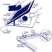
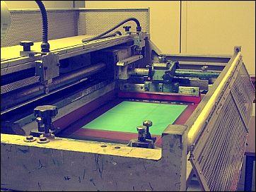
66 5. Printing Technology in OFETs Screen Printing

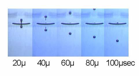
67 5. Printing Technology in OFETs Ink-Jet Printing


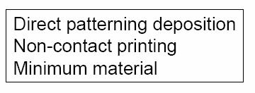
68 5. Printing Technology in OFETs Surface Energy Assisted Ink-Jet Printing

69 5. Printing Technology in OFETs Dip-Coating Ink-jet printing of wax is used to define the device structure
70 5. Printing Technology in OFETs Micro-contact Printing

71 5. Printing Technology in OFETs Micro-contact Printing

72 5. Printing Technology in OFETs Micro-contact Printing

73 5. Printing Technology in OFETs Roll-to-Roll Micro-contact Printing


74 5. Printing Technology in OFETs Micro-contact Printing OTFTs by Microcontact printing OLED by Microcontact printing E-ink by Microcontact printing


75 6. Future Prospects in OFETs Future Trend Molecular-Scale Electronic Devices Moore Moore s 1st st Law Moore s 2nd Law Chip functionality increases a factor of 4 every 3 years Manufacturing cost increases by a factor of 2 every 3 years Physics Today, 53, 38 (2000)

76 6. Future Prospects in OFETs CMOS Technology at 2010 Scaling of electron devices expects that only 8 electronsare required for on/off by 2010 Physics Today, 53, 38 (2000)

77 6. Future Prospects in OFETs Technology Roadmap SIA 2001

78 6. Future Prospects in OFETs How Can Go Beyond Roadmap? Nanostructures


79 6. Future Prospects in OFETs Top-Down and Bottom-Up Approach
80 6. Future Prospects in OFETs How Can Go Beyond Roadmap?
81 6. Future Prospects in OFETs Molecular Rectifier
82 6. Future Prospects in OFETs Molecular Rectifier
83 6. Future Prospects in OFETs Molecular Rectifier

84 6. Future Prospects in OFETs Single Molecular Transistor

85 6. Future Prospects in OFETs Nanotube Transistor Room Temperature CNTFET S.J. Tans et al., Nature, 393, 49 (1998)


86 6. Future Prospects in OFETs Fabrication Methods for Molecular Devices 1. E-Beam Lithography CNT


87 6. Future Prospects in OFETs Fabrication Methods for Molecular Devices 2. Nano Imprint Lithography
 is a scanning probe nano-patterning")

88 6. Future Prospects in OFETs Fabrication Methods for Molecular Devices 3. Dip-Pen Nanolithography Dip-PenNanolithography(DPN) is a scanning probe nano-patterning technique in which an AFM tip is used to deliver molecules to a surface via a solvent meniscus, which naturally forms in the ambient atmosphere. D. Piner, J. Zhu, F. Xu, and S. Hong, C. A. Mirkin, Science, 283, 661(1999)


89 6. Future Prospects in OFETs Fabrication Methods for Molecular Devices 4. Break Junction Single molecule transport studied in Mechanically Controllable Break Junctions M.A. Reed et al., Science 278, 252 (1997)


90 6. Future Prospects in OFETs Fabrication Methods for Molecular Devices 5. Self-Assembly Monolayer Self-AssembledMonolayer(SAM) A single layer of order molecules adsorbed on a substrate due to bonding b/w the surface and molecular head groups.-modification of adhesion-corrosion protection-chemical and biological functionalization-insulating layers in electronic devices


91 6. Future Prospects in OFETs Fabrication Methods for Molecular Devices 6. Langmuir-Blogett Deposition
92 6. Future Prospects in OFETs What Is Wrong with Si? Nothing! Smaller no Faster no Cheaper yes Polymers are NOT going to replace Si. Si processing is NOT cheap...low cost has been achieved through small size and high levels of integration. Packaging and placement are a large part of the cost of simple devices. In many applications the performance of Si is not required. There appears to be an opportunity that exists for a disruptive technology that has good enough performance and can achieve very low cost without regard to the size of the finished device

93 6. Future Prospects in OFETs Roadmap of Organic Electronics
Semiconductor Polymer
 Semiconductor Polymer Organic Semiconductor for Flexible Electronics Introduction: An organic semiconductor is an organic compound that possesses similar properties to inorganic semiconductors with hole
Initial Stages of Growth of Organic Semiconductors on Graphene
 Initial Stages of Growth of Organic Semiconductors on Graphene Presented by: Manisha Chhikara Supervisor: Prof. Dr. Gvido Bratina University of Nova Gorica Outline Introduction to Graphene Fabrication
Enhancing the Performance of Organic Thin-Film Transistor using a Buffer Layer
 Proceedings of the 9th International Conference on Properties and Applications of Dielectric Materials July 19-23, 29, Harbin, China L-7 Enhancing the Performance of Organic Thin-Film Transistor using
Fabrication Technology, Part I
 EEL5225: Principles of MEMS Transducers (Fall 2004) Fabrication Technology, Part I Agenda: Microfabrication Overview Basic semiconductor devices Materials Key processes Oxidation Thin-film Deposition Reading:
High speed vacuum deposition of organic TFTs in a roll-to-roll facility
 High speed vacuum deposition of organic TFTs in a roll-to-roll facility Dr Hazel Assender University of Oxford 1 Prof Martin Taylor Eifion Patchett, Aled Williams Prof Long Lin Prof Steve Yeates Dr John
Plastic Electronics. Joaquim Puigdollers.
 Plastic Electronics Joaquim Puigdollers Joaquim.puigdollers@upc.edu Nobel Prize Chemistry 2000 Origins Technological Interest First products.. MONOCROMATIC PHILIPS Today Future Technological interest Low
Fundamentals of the Metal Oxide Semiconductor Field-Effect Transistor
 Triode Working FET Fundamentals of the Metal Oxide Semiconductor Field-Effect Transistor The characteristics of energy bands as a function of applied voltage. Surface inversion. The expression for the
High Performance, Low Operating Voltage n-type Organic Field Effect Transistor Based on Inorganic-Organic Bilayer Dielectric System
 Journal of Physics: Conference Series PAPER OPEN ACCESS High Performance, Low Operating Voltage n-type Organic Field Effect Transistor Based on Inorganic-Organic Bilayer Dielectric System To cite this
Stretching the Barriers An analysis of MOSFET Scaling. Presenters (in order) Zeinab Mousavi Stephanie Teich-McGoldrick Aseem Jain Jaspreet Wadhwa
 Zeinab Mousavi Stephanie Teich-McGoldrick Aseem Jain Jaspreet Wadhwa") Stretching the Barriers An analysis of MOSFET Scaling Presenters (in order) Zeinab Mousavi Stephanie Teich-McGoldrick Aseem Jain Jaspreet Wadhwa Why Small? Higher Current Lower Gate Capacitance Higher
Stretching the Barriers An analysis of MOSFET Scaling Presenters (in order) Zeinab Mousavi Stephanie Teich-McGoldrick Aseem Jain Jaspreet Wadhwa Why Small? Higher Current Lower Gate Capacitance Higher
META-STABILITY EFFECTS IN ORGANIC BASED TRANSISTORS
 META-STABILITY EFFECTS IN ORGANIC BASED TRANSISTORS H. L. Gomes 1*, P. Stallinga 1, F. Dinelli 2, M. Murgia 2, F. Biscarini 2, D. M. de Leeuw 3 1 University of Algarve, Faculty of Sciences and Technology
Roll-to-roll manufacture of organic transistors for low cost circuits
 Roll-to-roll manufacture of organic transistors for low cost circuits Hazel Assender Dr Gamal Abbas, Ziqian Ding Department of Materials University of Oxford DALMATIAN TECHNOLOGY 21 st Sept 2011 1 Acknowledgements
Organic Electronic Devices
 Organic Electronic Devices Week 5: Organic Light-Emitting Devices and Emerging Technologies Lecture 5.5: Course Review and Summary Bryan W. Boudouris Chemical Engineering Purdue University 1 Understanding
Molecular Electronics For Fun and Profit(?)
") Molecular Electronics For Fun and Profit(?) Prof. Geoffrey Hutchison Department of Chemistry University of Pittsburgh geoffh@pitt.edu July 22, 2009 http://hutchison.chem.pitt.edu Moore s Law: Transistor
Molecular Electronics For Fun and Profit(?) Prof. Geoffrey Hutchison Department of Chemistry University of Pittsburgh geoffh@pitt.edu July 22, 2009 http://hutchison.chem.pitt.edu Moore s Law: Transistor
Semiconductor Physics Problems 2015
 Semiconductor Physics Problems 2015 Page and figure numbers refer to Semiconductor Devices Physics and Technology, 3rd edition, by SM Sze and M-K Lee 1. The purest semiconductor crystals it is possible
Metallic: 2n 1. +n 2. =3q Armchair structure always metallic = 2
 Properties of CNT d = 2.46 n 2 2 1 + n1n2 + n2 2π Metallic: 2n 1 +n 2 =3q Armchair structure always metallic a) Graphite Valence(π) and Conduction(π*) states touch at six points(fermi points) Carbon Nanotube:
There's Plenty of Room at the Bottom
 There's Plenty of Room at the Bottom 12/29/1959 Feynman asked why not put the entire Encyclopedia Britannica (24 volumes) on a pin head (requires atomic scale recording). He proposed to use electron microscope
Electronics with 2D Crystals: Scaling extender, or harbinger of new functions?
 Electronics with 2D Crystals: Scaling extender, or harbinger of new functions? 1 st Workshop on Data Abundant Systems Technology Stanford, April 2014 Debdeep Jena (djena@nd.edu) Electrical Engineering,
Supplementary Figure S1. AFM images of GraNRs grown with standard growth process. Each of these pictures show GraNRs prepared independently,
 Supplementary Figure S1. AFM images of GraNRs grown with standard growth process. Each of these pictures show GraNRs prepared independently, suggesting that the results is reproducible. Supplementary Figure
Supporting Information
 Supporting Information Oh et al. 10.1073/pnas.0811923106 SI Text Hysteresis of BPE-PTCDI MW-TFTs. Fig. S9 represents bidirectional transfer plots at V DS 100VinN 2 atmosphere for transistors constructed
Introducing the RoVaCBE Flagship project: Roll-to-roll Vacuum-processed Carbon Based Electronics. Dr Hazel Assender, University of Oxford
 Introducing the RoVaCBE Flagship project: Roll-to-roll Vacuum-processed Carbon Based Electronics Dr Hazel Assender, University of Oxford DALMATIAN TECHNOLOGY 21 st Sept 2010 1 Organic electronics Opportunity
an introduction to Semiconductor Devices
 an introduction to Semiconductor Devices Donald A. Neamen Chapter 6 Fundamentals of the Metal-Oxide-Semiconductor Field-Effect Transistor Introduction: Chapter 6 1. MOSFET Structure 2. MOS Capacitor -
ALL-POLYMER FET BASED ON SIMPLE PHOTOLITHOGRAPHIC MICRO-PATTERNING OF ELECTRICALLY CONDUCTING POLYMER
 Mol. Cryst. Liq. Cryst., Vol. 405, pp. 171 178, 2003 Copyright # Taylor & Francis Inc. ISSN: 1542-1406 print/1563-5287 online DOI: 10.1080/15421400390263541 ALL-POLYMER FET BASED ON SIMPLE PHOTOLITHOGRAPHIC
CMPEN 411 VLSI Digital Circuits. Lecture 03: MOS Transistor
 CMPEN 411 VLSI Digital Circuits Lecture 03: MOS Transistor Kyusun Choi [Adapted from Rabaey s Digital Integrated Circuits, Second Edition, 2003 J. Rabaey, A. Chandrakasan, B. Nikolic] CMPEN 411 L03 S.1
(a) (b) Supplementary Figure 1. (a) (b) (a) Supplementary Figure 2. (a) (b) (c) (d) (e)
 (b) Supplementary Figure 1. (a) (b) (a) Supplementary Figure 2. (a) (b) (c) (d) (e)") (a) (b) Supplementary Figure 1. (a) An AFM image of the device after the formation of the contact electrodes and the top gate dielectric Al 2 O 3. (b) A line scan performed along the white dashed line
(a) (b) Supplementary Figure 1. (a) An AFM image of the device after the formation of the contact electrodes and the top gate dielectric Al 2 O 3. (b) A line scan performed along the white dashed line
High-Performance Semiconducting Polythiophenes for Organic Thin Film. Transistors by Beng S. Ong,* Yiliang Wu, Ping Liu and Sandra Gardner
 Supplementary Materials for: High-Performance Semiconducting Polythiophenes for Organic Thin Film Transistors by Beng S. Ong,* Yiliang Wu, Ping Liu and Sandra Gardner 1. Materials and Instruments. All
Chapter 12: Electrical Properties. RA l
 Charge carriers and conduction: Chapter 12: Electrical Properties Charge carriers include all species capable of transporting electrical charge, including electrons, ions, and electron holes. The latter
UNIVERSITY OF CALIFORNIA College of Engineering Department of Electrical Engineering and Computer Sciences. Fall Exam 1
 UNIVERSITY OF CALIFORNIA College of Engineering Department of Electrical Engineering and Computer Sciences EECS 143 Fall 2008 Exam 1 Professor Ali Javey Answer Key Name: SID: 1337 Closed book. One sheet
MSE 310/ECE 340: Electrical Properties of Materials Fall 2014 Department of Materials Science and Engineering Boise State University
 MSE 310/ECE 340: Electrical Properties of Materials Fall 2014 Department of Materials Science and Engineering Boise State University Practice Final Exam 1 Read the questions carefully Label all figures
Chapter 3 Engineering Science for Microsystems Design and Fabrication
 Lectures on MEMS and MICROSYSTEMS DESIGN and MANUFACTURE Chapter 3 Engineering Science for Microsystems Design and Fabrication In this Chapter, we will present overviews of the principles of physical and
The Devices: MOS Transistors
 The Devices: MOS Transistors References: Semiconductor Device Fundamentals, R. F. Pierret, Addison-Wesley Digital Integrated Circuits: A Design Perspective, J. Rabaey et.al. Prentice Hall NMOS Transistor
ESE 570: Digital Integrated Circuits and VLSI Fundamentals
 ESE 570: Digital Integrated Circuits and VLSI Fundamentals Lec 4: January 23, 2018 MOS Transistor Theory, MOS Model Penn ESE 570 Spring 2018 Khanna Lecture Outline! CMOS Process Enhancements! Semiconductor
Halbleiter Prof. Yong Lei Prof. Thomas Hannappel
 Halbleiter Prof. Yong Lei Prof. Thomas Hannappel yong.lei@tu-ilmenau.de thomas.hannappel@tu-ilmenau.de http://www.tu-ilmenau.de/nanostruk/ Organic Semiconductors & Organic Electronics Organic semiconductors
MOS Transistor I-V Characteristics and Parasitics
 ECEN454 Digital Integrated Circuit Design MOS Transistor I-V Characteristics and Parasitics ECEN 454 Facts about Transistors So far, we have treated transistors as ideal switches An ON transistor passes
EECS130 Integrated Circuit Devices
 EECS130 Integrated Circuit Devices Professor Ali Javey 10/30/2007 MOSFETs Lecture 4 Reading: Chapter 17, 19 Announcements The next HW set is due on Thursday. Midterm 2 is next week!!!! Threshold and Subthreshold
Section 12: Intro to Devices
 Section 12: Intro to Devices Extensive reading materials on reserve, including Robert F. Pierret, Semiconductor Device Fundamentals EE143 Ali Javey Bond Model of Electrons and Holes Si Si Si Si Si Si Si
Classification of Solids
 Classification of Solids Classification by conductivity, which is related to the band structure: (Filled bands are shown dark; D(E) = Density of states) Class Electron Density Density of States D(E) Examples
Section 12: Intro to Devices
 Section 12: Intro to Devices Extensive reading materials on reserve, including Robert F. Pierret, Semiconductor Device Fundamentals Bond Model of Electrons and Holes Si Si Si Si Si Si Si Si Si Silicon
Scaling Issues in Planar FET: Dual Gate FET and FinFETs
 Scaling Issues in Planar FET: Dual Gate FET and FinFETs Lecture 12 Dr. Amr Bayoumi Fall 2014 Advanced Devices (EC760) Arab Academy for Science and Technology - Cairo 1 Outline Scaling Issues for Planar
Lecture 18 Field-Effect Transistors 3
 Lecture 18 Field-Effect Transistors 3 Schroder: Chapters, 4, 6 1/38 Announcements Homework 4/6: Is online now. Due Today. I will return it next Wednesday (30 th May). Homework 5/6: It will be online later
Final Examination EE 130 December 16, 1997 Time allotted: 180 minutes
 Final Examination EE 130 December 16, 1997 Time allotted: 180 minutes Problem 1: Semiconductor Fundamentals [30 points] A uniformly doped silicon sample of length 100µm and cross-sectional area 100µm 2
Supporting Information
 Supporting Information Monolithically Integrated Flexible Black Phosphorus Complementary Inverter Circuits Yuanda Liu, and Kah-Wee Ang* Department of Electrical and Computer Engineering National University
ECE 340 Lecture 39 : MOS Capacitor II
 ECE 340 Lecture 39 : MOS Capacitor II Class Outline: Effects of Real Surfaces Threshold Voltage MOS Capacitance-Voltage Analysis Things you should know when you leave Key Questions What are the effects
MOSFET: Introduction
 E&CE 437 Integrated VLSI Systems MOS Transistor 1 of 30 MOSFET: Introduction Metal oxide semiconductor field effect transistor (MOSFET) or MOS is widely used for implementing digital designs Its major
L ECE 4211 UConn F. Jain Scaling Laws for NanoFETs Chapter 10 Logic Gate Scaling
 L13 04202017 ECE 4211 UConn F. Jain Scaling Laws for NanoFETs Chapter 10 Logic Gate Scaling Scaling laws: Generalized scaling (GS) p. 610 Design steps p.613 Nanotransistor issues (page 626) Degradation
12/10/09. Chapter 18: Electrical Properties. View of an Integrated Circuit. Electrical Conduction ISSUES TO ADDRESS...
 Chapter 18: Electrical Properties ISSUES TO ADDRESS... How are electrical conductance and resistance characterized? What are the physical phenomena that distinguish? For metals, how is affected by and
Electronic Supplementary Information. Molecular Antenna Tailored Organic Thin-film Transistor for. Sensing Application
 Electronic Supplementary Material (ESI) for Materials Horizons. This journal is The Royal Society of Chemistry 2017 Electronic Supplementary Information Molecular Antenna Tailored Organic Thin-film Transistor
Lecture 12: MOS Capacitors, transistors. Context
 Lecture 12: MOS Capacitors, transistors Context In the last lecture, we discussed PN diodes, and the depletion layer into semiconductor surfaces. Small signal models In this lecture, we will apply those
GaN based transistors
 GaN based transistors S FP FP dielectric G SiO 2 Al x Ga 1-x N barrier i-gan Buffer i-sic D Transistors "The Transistor was probably the most important invention of the 20th Century The American Institute
Supporting Information
 Electronic Supplementary Material (ESI) for ChemComm. This journal is The Royal Society of Chemistry 2014 Supporting Information High-k Polymer/Graphene Oxide Dielectrics for Low-Voltage Flexible Nonvolatile
Supplementary Figure 1 Experimental setup for crystal growth. Schematic drawing of the experimental setup for C 8 -BTBT crystal growth.
 Supplementary Figure 1 Experimental setup for crystal growth. Schematic drawing of the experimental setup for C 8 -BTBT crystal growth. Supplementary Figure 2 AFM study of the C 8 -BTBT crystal growth
ISSUES TO ADDRESS...
 Chapter 12: Electrical Properties School of Mechanical Engineering Choi, Hae-Jin Materials Science - Prof. Choi, Hae-Jin Chapter 12-1 ISSUES TO ADDRESS... How are electrical conductance and resistance
Supporting Online Material for
 www.sciencemag.org/cgi/content/full/327/5966/662/dc Supporting Online Material for 00-GHz Transistors from Wafer-Scale Epitaxial Graphene Y.-M. Lin,* C. Dimitrakopoulos, K. A. Jenkins, D. B. Farmer, H.-Y.
Keywords: thin-film transistors, organic polymers, bias temperature stress, electrical instabilities, transient regime.
 Time dependence of organic polymer thin-film transistors current Sandrine Martin *, Laurence Dassas, Michael C. Hamilton and Jerzy Kanicki University of Michigan, Solid-State Electronics Laboratory, Department
Electric Field-Dependent Charge-Carrier Velocity in Semiconducting Carbon. Nanotubes. Yung-Fu Chen and M. S. Fuhrer
 Electric Field-Dependent Charge-Carrier Velocity in Semiconducting Carbon Nanotubes Yung-Fu Chen and M. S. Fuhrer Department of Physics and Center for Superconductivity Research, University of Maryland,
Semiconductor Physics fall 2012 problems
 Semiconductor Physics fall 2012 problems 1. An n-type sample of silicon has a uniform density N D = 10 16 atoms cm -3 of arsenic, and a p-type silicon sample has N A = 10 15 atoms cm -3 of boron. For each
1 Name: Student number: DEPARTMENT OF PHYSICS AND PHYSICAL OCEANOGRAPHY MEMORIAL UNIVERSITY OF NEWFOUNDLAND. Fall :00-11:00
 1 Name: DEPARTMENT OF PHYSICS AND PHYSICAL OCEANOGRAPHY MEMORIAL UNIVERSITY OF NEWFOUNDLAND Final Exam Physics 3000 December 11, 2012 Fall 2012 9:00-11:00 INSTRUCTIONS: 1. Answer all seven (7) questions.
ESE370: Circuit-Level Modeling, Design, and Optimization for Digital Systems
 ESE370: Circuit-Level Modeling, Design, and Optimization for Digital Systems Lec 6: September 14, 2015 MOS Model You are Here: Transistor Edition! Previously: simple models (0 and 1 st order) " Comfortable
MOS CAPACITOR AND MOSFET
 EE336 Semiconductor Devices 1 MOS CAPACITOR AND MOSFET Dr. Mohammed M. Farag Ideal MOS Capacitor Semiconductor Devices Physics and Technology Chapter 5 EE336 Semiconductor Devices 2 MOS Capacitor Structure
Theory of Electrical Characterization of Semiconductors
 Theory of Electrical Characterization of Semiconductors P. Stallinga Universidade do Algarve U.C.E.H. A.D.E.E.C. OptoElectronics SELOA Summer School May 2000, Bologna (It) Overview Devices: bulk Schottky
Low Frequency Noise in MoS 2 Negative Capacitance Field-effect Transistor
 Low Frequency Noise in MoS Negative Capacitance Field-effect Transistor Sami Alghamdi, Mengwei Si, Lingming Yang, and Peide D. Ye* School of Electrical and Computer Engineering Purdue University West Lafayette,
ESE 570: Digital Integrated Circuits and VLSI Fundamentals
 ESE 570: Digital Integrated Circuits and VLSI Fundamentals Lec 4: January 29, 2019 MOS Transistor Theory, MOS Model Penn ESE 570 Spring 2019 Khanna Lecture Outline! CMOS Process Enhancements! Semiconductor
FIELD-EFFECT TRANSISTORS
 FIEL-EFFECT TRANSISTORS 1 Semiconductor review 2 The MOS capacitor 2 The enhancement-type N-MOS transistor 3 I-V characteristics of enhancement MOSFETS 4 The output characteristic of the MOSFET in saturation
Semiconductor Detectors
 Semiconductor Detectors Summary of Last Lecture Band structure in Solids: Conduction band Conduction band thermal conductivity: E g > 5 ev Valence band Insulator Charge carrier in conductor: e - Charge
MOS Transistors. Prof. Krishna Saraswat. Department of Electrical Engineering Stanford University Stanford, CA
 MOS Transistors Prof. Krishna Saraswat Department of Electrical Engineering S Stanford, CA 94305 saraswat@stanford.edu 1 1930: Patent on the Field-Effect Transistor! Julius Lilienfeld filed a patent describing
Challenges and Opportunities. Prof. J. Raynien Kwo 年
 Nanoelectronics Beyond Si: Challenges and Opportunities Prof. J. Raynien Kwo 年 立 Si CMOS Device Scaling Beyond 22 nm node High κ,, Metal gates, and High mobility channel 1947 First Transistor 1960 1960
Organic solar cells. State of the art and outlooks. Gilles Horowitz LPICM, UMR7647 CNRS - Ecole Polytechnique
 Organic solar cells. State of the art and outlooks Gilles Horowitz LPICM, UMR7647 CNRS - Ecole Polytechnique Solar energy Solar energy on earth: 75,000 tep/year 6000 times the world consumption in 2007
SUPPLEMENTARY INFORMATION
 doi:.38/nature09979 I. Graphene material growth and transistor fabrication Top-gated graphene RF transistors were fabricated based on chemical vapor deposition (CVD) grown graphene on copper (Cu). Cu foil
Nanoelectronics. Topics
 Nanoelectronics Topics Moore s Law Inorganic nanoelectronic devices Resonant tunneling Quantum dots Single electron transistors Motivation for molecular electronics The review article Overview of Nanoelectronic
Plasma Deposition (Overview) Lecture 1
 Lecture 1") Plasma Deposition (Overview) Lecture 1 Material Processes Plasma Processing Plasma-assisted Deposition Implantation Surface Modification Development of Plasma-based processing Microelectronics needs (fabrication
Plasma Deposition (Overview) Lecture 1 Material Processes Plasma Processing Plasma-assisted Deposition Implantation Surface Modification Development of Plasma-based processing Microelectronics needs (fabrication
Metal-oxide-semiconductor field effect transistors (2 lectures)
") Metal-ide-semiconductor field effect transistors ( lectures) MOS physics (brief in book) Current-voltage characteristics - pinch-off / channel length modulation - weak inversion - velocity saturation -
Metal-ide-semiconductor field effect transistors ( lectures) MOS physics (brief in book) Current-voltage characteristics - pinch-off / channel length modulation - weak inversion - velocity saturation -
CVD: General considerations.
 CVD: General considerations. PVD: Move material from bulk to thin film form. Limited primarily to metals or simple materials. Limited by thermal stability/vapor pressure considerations. Typically requires
Synthesis Breakout. Overarching Issues
 Synthesis Breakout. Overarching Issues 1. What are fundamental structural and electronic factors limiting Jsc, Voc, and FF in typical polymer bulk-heterojunction cells? Rational P- and N-type materials
Negative Bias Temperature Instability (NBTI) Physics, Materials, Process, and Circuit Issues. Dieter K. Schroder Arizona State University Tempe, AZ
 Physics, Materials, Process, and Circuit Issues. Dieter K. Schroder Arizona State University Tempe, AZ") Negative Bias Temperature Instability (NBTI) Physics, Materials, Process, and Circuit Issues Dieter K. Schroder Arizona State University Tempe, AZ Introduction What is NBTI? Material Issues Device Issues
Negative Bias Temperature Instability (NBTI) Physics, Materials, Process, and Circuit Issues Dieter K. Schroder Arizona State University Tempe, AZ Introduction What is NBTI? Material Issues Device Issues
Supporting Information
 Electronic Supplementary Material (ESI) for Nanoscale. This journal is The Royal Society of Chemistry 2016 Supporting Information Graphene transfer method 1 : Monolayer graphene was pre-deposited on both
Dielectric materials for Organic Thin-Film Transistors
 Dielectric materials for Organic Thin-Film Transistors Arinola Awomolo University of Illinois Chicago Advisors: : Prof. Christos Takoudis, Prof. Greg Jursich Graduate Research Assistant: Lin Jiang Motorola
High-Mobility n-channel Organic Field Effect Transistors based on Epitaxially Grown C 60 Films
 High-Mobility n-channel Organic Field Effect Transistors based on Epitaxially Grown C 60 Films Th. B. Singh, N. Marjanović, G. J. Matt, S. Günes and N. S. Sariciftci Linz Institute for Organic Solar Cells
CMOS Scaling. Two motivations to scale down. Faster transistors, both digital and analog. To pack more functionality per area. Lower the cost!
 Two motivations to scale down CMOS Scaling Faster transistors, both digital and analog To pack more functionality per area. Lower the cost! (which makes (some) physical sense) Scale all dimensions and
Self-Assembly in Organic Thin Film Transistors for Flexible Electronic Devices
 Page 1 of 6 Page 1 of 6 Return to Web Version Self-Assembly in Organic Thin Film Transistors for Flexible Electronic Devices By: Professor Zhenan Bao, Material Matters 2006, 1.2, 11. Department of Chemical
! CMOS Process Enhancements. ! Semiconductor Physics. " Band gaps. " Field Effects. ! MOS Physics. " Cut-off. " Depletion.
 ESE 570: Digital Integrated Circuits and VLSI Fundamentals Lec 4: January 3, 018 MOS Transistor Theory, MOS Model Lecture Outline! CMOS Process Enhancements! Semiconductor Physics " Band gaps " Field Effects!
CHAPTER 5 EFFECT OF GATE ELECTRODE WORK FUNCTION VARIATION ON DC AND AC PARAMETERS IN CONVENTIONAL AND JUNCTIONLESS FINFETS
 98 CHAPTER 5 EFFECT OF GATE ELECTRODE WORK FUNCTION VARIATION ON DC AND AC PARAMETERS IN CONVENTIONAL AND JUNCTIONLESS FINFETS In this chapter, the effect of gate electrode work function variation on DC
Materials Chemistry for Organic Electronics and Photonics
 Materials Chemistry for Organic Electronics and Photonics Prof. Dong-Yu Kim Photonics Polymer Laboratory Dept. of Materials Science and Engineering Gwangju Institute of Science and Technology kimdy@gist.ac.kr,
Lecture 5: CMOS Transistor Theory
 Lecture 5: CMOS Transistor Theory Slides courtesy of Deming Chen Slides based on the initial set from David Harris CMOS VLSI Design Outline q q q q q q q Introduction MOS Capacitor nmos I-V Characteristics
UNIVERSITY OF CALIFORNIA College of Engineering Department of Electrical Engineering and Computer Sciences. Professor Chenming Hu.
 UNIVERSITY OF CALIFORNIA College of Engineering Department of Electrical Engineering and Computer Sciences EECS 130 Spring 2009 Professor Chenming Hu Midterm I Name: Closed book. One sheet of notes is
Self-study problems and questions Processing and Device Technology, FFF110/FYSD13
 Self-study problems and questions Processing and Device Technology, FFF110/FYSD13 Version 2016_01 In addition to the problems discussed at the seminars and at the lectures, you can use this set of problems
Nanoparticle Memories: CMOS, Organic and Hybrid approaches
 Nanoparticle Memories: CMOS, Organic and Hybrid approaches Panagiotis Dimitrakis, Ph.D IMEL/NCSR Demokritos Winter School on Nanoelectronic and Nanophotonics Bilkent University Ankara, Turkey 19-25 January
The Devices. Digital Integrated Circuits A Design Perspective. Jan M. Rabaey Anantha Chandrakasan Borivoje Nikolic. July 30, 2002
 Digital Integrated Circuits A Design Perspective Jan M. Rabaey Anantha Chandrakasan Borivoje Nikolic The Devices July 30, 2002 Goal of this chapter Present intuitive understanding of device operation Introduction
Chapter 3 Basics Semiconductor Devices and Processing
 Chapter 3 Basics Semiconductor Devices and Processing Hong Xiao, Ph. D. www2.austin.cc.tx.us/hongxiao/book.htm Hong Xiao, Ph. D. www2.austin.cc.tx.us/hongxiao/book.htm 1 Objectives Identify at least two
ESE370: Circuit-Level Modeling, Design, and Optimization for Digital Systems
 ESE370: Circuit-Level Modeling, Design, and Optimization for Digital Systems Lec 6: September 18, 2017 MOS Model You are Here: Transistor Edition! Previously: simple models (0 and 1 st order) " Comfortable
The Devices. Jan M. Rabaey
 The Devices Jan M. Rabaey Goal of this chapter Present intuitive understanding of device operation Introduction of basic device equations Introduction of models for manual analysis Introduction of models
MENA9510 characterization course: Capacitance-voltage (CV) measurements
 measurements") MENA9510 characterization course: Capacitance-voltage (CV) measurements 30.10.2017 Halvard Haug Outline Overview of interesting sample structures Ohmic and schottky contacts Why C-V for solar cells? The
MENA9510 characterization course: Capacitance-voltage (CV) measurements 30.10.2017 Halvard Haug Outline Overview of interesting sample structures Ohmic and schottky contacts Why C-V for solar cells? The
Electrical characterization of polymer ferroelectric diodes
 Electrical characterization of polymer ferroelectric diodes Reza Saberi Moghaddam July 2010 Supervisors: Prof. Dr. Dago. M. de Leeuw Prof. Dr. Ir. P. W. M. Blom Dr. K. Asadi Molecular Electronics, Physics
Long Channel MOS Transistors
 Long Channel MOS Transistors The theory developed for MOS capacitor (HO #2) can be directly extended to Metal-Oxide-Semiconductor Field-Effect transistors (MOSFET) by considering the following structure:
Lecture 2 Thin Film Transistors
 Lecture 2 Thin Film Transistors 1/60 Announcements Homework 1/4: Will be online after the Lecture on Tuesday October 2 nd. Total of 25 marks. Each homework contributes an equal weight. All homework contributes
The Intrinsic Silicon
 The Intrinsic ilicon Thermally generated electrons and holes Carrier concentration p i =n i ni=1.45x10 10 cm-3 @ room temp Generally: n i = 3.1X10 16 T 3/2 e -1.21/2KT cm -3 T= temperature in K o (egrees
UNIVERSITY OF CALIFORNIA College of Engineering Department of Electrical Engineering and Computer Sciences. EECS 130 Professor Ali Javey Fall 2006
 UNIVERSITY OF CALIFORNIA College of Engineering Department of Electrical Engineering and Computer Sciences EECS 130 Professor Ali Javey Fall 2006 Midterm 2 Name: SID: Closed book. Two sheets of notes are
MOS Transistor Theory
 CHAPTER 3 MOS Transistor Theory Outline 2 1. Introduction 2. Ideal I-V Characteristics 3. Nonideal I-V Effects 4. C-V Characteristics 5. DC Transfer Characteristics 6. Switch-level RC Delay Models MOS
Gold Nanoparticles Floating Gate MISFET for Non-Volatile Memory Applications
 Gold Nanoparticles Floating Gate MISFET for Non-Volatile Memory Applications D. Tsoukalas, S. Kolliopoulou, P. Dimitrakis, P. Normand Institute of Microelectronics, NCSR Demokritos, Athens, Greece S. Paul,
Research Opportunities in Macroelectronics. Motivation, Application Overview. Materials Classes, Challenges. Patterning Techniques, Challenges
 Research Opportunities in Macroelectronics Motivation, Application Overview Materials Classes, Challenges Patterning Techniques, Challenges John A. Rogers -- University of Illinois at Urbana/Champaign
! Previously: simple models (0 and 1 st order) " Comfortable with basic functions and circuits. ! This week and next (4 lectures)
 Comfortable with basic functions and circuits. ! This week and next (4 lectures)") ESE370: CircuitLevel Modeling, Design, and Optimization for Digital Systems Lec 6: September 14, 2015 MOS Model You are Here: Transistor Edition! Previously: simple models (0 and 1 st order) " Comfortable
ESE370: CircuitLevel Modeling, Design, and Optimization for Digital Systems Lec 6: September 14, 2015 MOS Model You are Here: Transistor Edition! Previously: simple models (0 and 1 st order) " Comfortable
SEMINAR. Organic Semiconductor Thin Film Transistors
 University of Ljubljana Faculty of Mathematics and Physics Department of Physics SEMINAR Organic Semiconductor Thin Film Transistors Author: Tomaž Mlakar Adviser: Dr. Gvido Bratina Nova Gorica Polytechnic