Performance of semi-insulating. insulating GaAs-based radiation detectors: Role of key physical parameters of base material
|
|
|
- Marian Wilson
- 5 years ago
- Views:
Transcription

1 Institute of Electrical Engineering Slovak Academy of Sciences, Bratislava Slovak republic Performance of semi-insulating insulating GaAs-based radiation detectors: Role of key physical parameters of base material F. Dubecký IEE SAS, Bratislava, Slovakia PISA, ITALY V. Nečas IEEIT SIT, Bratislava, Slovakia C. Ferrari IMEM C.N.R., Parma, Italy
2 MOTIVATION RADIATION DETECTOR CHARACTERISTICS Key detector-grade material aspects APPLICATIONS Monolithic LEC SI GaAs strip line in edge-on configuration Line concept of SI GaAs chip First quantum X-ray images Quantum X-CT: preliminary GaAs MATERIAL FOR RADIATION DETECTORS Key material characteristics Characteristics summary Performances of fabricated detectors CONCLUSIONS OUTLINE
3 Motivation I: New applications of semiconductor monolithic array detectors in X- and gamma-ray detection NEW DETECTOR APPLICATIONS BASIC KNOWLEDGE: Experiments in physics X-ray astronomy. 115 InP: Solar neutrino astrophysics MEDICINE Digital X-ray radiology (stomatology, mammography), XCT Positron emission tomography NONDESTRUCTIVE ON-LINE CONTROL Material defect and process control SECURITY Contraband inspections: cargo control Detection of drugs and plastic explosives Cultural heritage s study MONITORING Environmental control and radioactive waste management Metrology (testing of radioactive sources, spectrometry...) IMPROVEMENTS IN X-RAY DIGITAL RADIOLOGY USING SEMICONDUCTOR DETECTORS LOWER DOSE TO PATIENT MUCH BETTER RESOLUTION IN CONTRAST (more than 2 orders of magnitude) DETERMINATION OF THE OBJECT DENSITY (Dual X-ray or colour imaging technique) 3-D IMAGE POSSIBLE USING CT METHOD NO POLUTION DUE TO CHEMICAL PROCESSING (Necessary in the case of film application) SIMPLE AND SPACE SAVING STORAGE OF DIGITAL DATA ON-LINE PROCESS CONTROL & DIAGNOSTICS OTHERS...???


4 COLOUR IMAGING in digital radiography A+B A B A, B: Dual energy digital radiographs
5 MOTIVATION II Radiation hard Low cost Fast SI GaAs MATERIAL PROPERTIES Wide band gap allows operation at RT Highly developed technology processing Easily commercially available Bulk material no limitation in thickness LINE (2D) SCANNING TECHNIQUE IN RADIOGRAPHIC IMAGING Quantum XCT Technical simplest imaging solution Lowest cost Useful for fast testing of detector applicability in X-ray imaging High quality of X-ray image (good scattered photons rejection) Useful in many industrial, medical and security applications Applicable in basic and space research HIGH QUALITY!!
, high v d, µ d high homogeneity, low density of structural, space-charge and point defects, fast reaction LOW COST CANDIDATE SEMICONDUCTORS 3-3 kev CdTe II-VI: CdTe, CdZnTe, HgI 2,")
6 Key semiconductor material and detector characteristics REQUIREMENTS TO SEMICONDUCTOR DETECTOR-GRADE MATERIAL Z > 3; E G > 1.3 ev, τ, ρ (RT), high v d, µ d high homogeneity, low density of structural, space-charge and point defects, fast reaction LOW COST CANDIDATE SEMICONDUCTORS 3-3 kev CdTe II-VI: CdTe, CdZnTe, HgI 2, III-V: GaAs, InP,?? GaP, GaN, OUT OF INTEREST: Si, Ge Linear attenuation coef. Bulk InP Bulk GaAs Silicon Zn x Cd 1-x Te Volume price per attenuation
7 Important material aspect: Attenuation coefficient A Z 4 5 Photon attenuation coefficent µ, cm GaAs InP CdTe Photon energy, kev


8 SI GaAs X- and gamma ray line detector: New topology 23 Type of developed line SI GaAs detector Number of strips in line Pitch, mm Absorption length, mm Chip dimensions, mm Effective absorption volume of strip, mm 3 Maximal thickness of substrate base, mm SAMO X ,25,125/,25*,125 2,5 16x3,5 16x3,5/32x3,5* 32x3,5,6,4/,8,4,12,18 SAMO XS ,25 2,5** 8x3,5,1,18,2,3 TOP side BACK side Trenches using RIE Conductive carrier


, final")
.")


9 SI GaAs line X-ray detector chip mounted onto flexible PCB carrier: Original concept (top), final arrangement (down).25 mm thick flexible PCB holder GaAs line detector chip Micro-Peltier Heat sink
10 SI GaAs DETECTOR APPLICATIONS SINGLE PHOTON COUNTING = QUANTUM X-RAY SCANNER QUANTUM X-CT: FIRST EXAMPLE


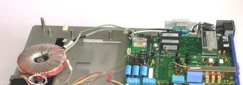


11 Portable digital X-ray scanner based on SI GaAs radiation detectors: Final set-up consists of 48 channels line, position control and communication


12 Photos of various selected test objects


13 QUANTUM X-ray digital images of test objects LINE STEP:.25 mm


14 Testing X-CT platform Observed gamma-ray projection 55 Početnosť Pozícia, mm Fe tube wood Test object Fe pin Cu
15 GaAs detectors testing: fluctuations in counting FPN Sigma Nápočet Fotónový šum Ručné meranie detektoru D1 Automatické meranie detektoru D1 Automatické meranie detektoru D2 Výskyt početnosti Data: NAPOCET77_B Model: Gauss Chi^2 = R^2 =.9871 y ± xc ± w ±1.81 A ± Početnosť Requirements to SI GaAs detectors based on detector grade materials From the point of view statistical fluctuations: Poisson s limit: S/N = (n) 1/2 Other goals: - production yield - stability in long-term operation - high homogeneity
16 SI GaAs Role of key physical parameters of base materials
17 GDMS analysis: SI GaAs materials Element Sample label A1 B C D1 D2 E F G H K L M* B n/a 2 56 Na <1.5 <2 <1.7 4 <2 8 3 <2 4 <1.5 3 Mg <2 <2 <2 <2 <2 4 <1.9 <1.9 5 <1.5 <2 Al <1 3 <1 14 < <1 9 Si <3 11 < <3 445 P <3 < < < <3 11 S < < Cl < Ti <.4 2 <.4 3 <.5 <.5 1 <.4 1 <.4 <.4 Cr <1.2 <1.2 <1.2 <1 <1 <1 <1.2 <1.2 7 <.9 <1.5 Fe <.4 1 < <.4 8 Cu <2.5 <3 < <3 <3 <2.5 <3 <2.5 <2.7 Total: <447 <594 <312 <1515 <1258 <86 <576 <36 <953 <257 >6655 Following impurities were obtained in all samples under given detection limit: F<25, Li<6, Be<5, K<25, Ca<2, Mn<.5, Ni<1.1, Zn<4, Ge<4, Se<13, Mo<1.8, Cd<.5, In<1, Sn<4, Te<2, Sb<2, Pb<.5, Bi<.5. NOTICES: In the analysis there are not included C, N 2, O 2 as the background contaminants in GDMS and host atoms, Ga and As. *Content of other important impurities (ppb at.) in the sample M is following: F 35, Mn 5, and Te 32.
18 Detection performance: SI GaAs detectors Counts per channel Counts per channel Channel V -14V -12V -9V -21V -18V -15V SI GaAs: Sample Co-57 SI GaAs: Sample RT Co Channel Counts per channel Counts per channel V -18V -15V SI GaAs: Sample RT Co V -9 V Channel SI GaAs: Sample RT Co-57-21V Channel Counts per channel Counts per channel V SI GaAs: Sample RT Co-57-15V Channel V -9V SI GaAs: Sample RT Co-57-15V Channel 7 Counts per channel Counts per channel V -18V -15V SI GaAs: Sample RT Co Channel Channel 2-3V - 25V SI GaAs: Sample RT Co-57-12V -18V?? Counts per channel V -2V -15V SI GaAs: Sample Co-57-25V Counts per channel SI GaAs: Sample RT Co-57-21V -15V -12V -9V Counts per channel SI GaAs: Sample RT Co V Counts per channel V - 3 V SI GaAs: Sample RT Co Channel Channel Channel Counts

 grown")


19 High resolution DCT and LST: SI GaAs materials a) SI GaAs: LEC (B) and VGF (D1) grown materials. Material FWHM DCT PD, DD, cm -2 cm -3 LST B LEC 7.2 2x1 4 n/a D1 VGF x1 7 4x1 3 a/

20 Capacitance study: SI GaAs detectors N/A??
21 Basic electrical and material characteristics and detectors performances: SI GaAs materials SUMMARY Tabe 1. Information about bulk SI GaAs wafers and detection performances to 122 kev γ-radiation. Sample label Growth Method Doping, contamination EPD cm -2 Resistivity Ωcm (RT) Hall mobility cm 2 /Vs (RT) Detection performances (RT) CCE, % HWHM, % P/V A1 LEC Non <6x x B LEC Non, Ti <4x x C LEC Non <4x x D1 VGF Non, Cu, Fe, <5x x Ti D2 VGF Non, Cu, Fe <4x x E HP LEC Non <6x x F LP LEC Non <2x x G LEC Non <8x x no photopeak detected H LEC Cr <1x x K LEC Non <2x x no photopeak?? detected L LEC Non <6x x M LEC Non <8x x no photopeak detected


22 EBIC: SI GaAs SE Bias voltage: -3 V -6 V E: M/A COM HP LEC SI GaAs F: M/A COM LP LEC SI GaAs Detector contact: 2 mm diameter Base thickness: 2 µm
23 1 1 T = 298 K I-V characteristic of SI GaAs detector with the Schottky barrier?? Explanation of the second current saturation region observed at the reverse I-V characteristics Au bulk SI GaAs LTG MBE GaAs buffer Au/Ge/Ni Current, na 1,1,1 1E-3 bulk limited ohmic transport 1E-3,1, Bias voltage, V I S? Reverse Forward Thermiionic emission current via Schottky barrier q( V IR ) I I S = I = S e AA ** T nkt 2 e S qφb kt 1 Saturation current
24 I-V characteristics of SI GaAs detectors with the Schottky barrier (2 mm diameter) Baldini, R., et al., NIM A 449 (2) 268
25 Pulse-height spectra of 241 Am anda 57 Co detected by dedicated SI GaAs PAD detector Counts per channel L α (Np) L β (Np) 14. kev 17.7 kev 14.4 kev L γ (Np) 2.8 kev 26.3 kev 33.2 kev 59.5 kev K α (Pb) 75. kev K β (Pb) 84.9 kev SI GaAs: ITME 16 µm, φ =.5 mm 241 Am, 57 Co, RT Bias = - 25 V kev kev K α (Ag) 22.2 kev * Energy, kev B. Zaťko at al.: Nucl. Instr. Meth. A (24)
 111 Energy resolution in FWHM, kev 25 2 15 1 5 SI GaAs: Different results 241 Am: 59.")
26 P + SI GaAs detectors structure Au/Zn P ++ GaAs(Be) (2x1 18 cm -3 ) P + GaAs(Be) (2x1 18 cm -3 ) bulk SI GaAs Au/Ge/Ni Schottky barrier Optimization of the ohmic and blocking SI GaAs detector contacts Au bulk SI GaAs LTG MBE GaAs buffer Au/Ge/Ni Zaťko, B., et al., NIM A531 (24) 111 Energy resolution in FWHM, kev SI GaAs: Different results 241 Am: K B E D A L P P 1E-3,1,1 1 L D J K L L F P P D C P Detector volume, mm 3 M G N H electronic noise I Base width: 13 µm 25 µm 4 µm 16 µm Literatu A 2 µm B VPE 7 µm C 1 µm D 2 µm E 7 µm F 8 µm G 2 µm H 35 µm I 63 µm J 13 µm K 8 µm L 3 µm M 6 µm N 2 µm P 2 µm
27 Conclusions Bulk SI GaAs: Radiation detector-grade material is available on the market! Key material characteristics: - preferable VGF, low dislocation density - high chemical purity (GDMS) - RT Hall mobility > 65 cm 2 /Vs - RT resistivity (.8 3)e7 ohm cm Following material evaluation tools: X-ray topography, LST, PL, Detector evaluation tools: I-V, C-V, EBIC, pulse height spectra,... Detector electrodes: Must be optimized for required performance Schottky back-to-back electrode technology: Potential improvement must be investigated in more details!! PERSPECTIVE APPLICATIONS: Quantum X-RAY IMAGING, Quantum X-CT, BASIC & SPACE RESEARCH: PLASMA DIAGNOSTIC IN NUCLEAR FUSSION
28 THANK YOU FOR YOUR ATTENTION!!!
Outline. Introduction, motivation Readout electronics, Peltier cooling Input J-FETsJ
 Progress in low energy X-rayX spectroscopy using semi-insulating insulating GaAs detectors F. Dubecký 1, B. Zaťko 1, P. Boháček 1, L. Ryć 2, E. Gombia 2, and V. Nečas 3 1 IEE SAS, Bratislava, Slovakia
Semiconductor Detectors
 Semiconductor Detectors Summary of Last Lecture Band structure in Solids: Conduction band Conduction band thermal conductivity: E g > 5 ev Valence band Insulator Charge carrier in conductor: e - Charge
Advantages / Disadvantages of semiconductor detectors
 Advantages / Disadvantages of semiconductor detectors Semiconductor detectors have a high density (compared to gas detector) large energy loss in a short distance diffusion effect is smaller than in gas
EE 5344 Introduction to MEMS CHAPTER 5 Radiation Sensors
 EE 5344 Introduction to MEMS CHAPTER 5 Radiation Sensors 5. Radiation Microsensors Radiation µ-sensors convert incident radiant signals into standard electrical out put signals. Radiant Signals Classification
Semiconductor X-Ray Detectors. Tobias Eggert Ketek GmbH
 Semiconductor X-Ray Detectors Tobias Eggert Ketek GmbH Semiconductor X-Ray Detectors Part A Principles of Semiconductor Detectors 1. Basic Principles 2. Typical Applications 3. Planar Technology 4. Read-out
Pixels GaAs Detectors for Digital Radiography. M.E. Fantacci. and. Abstract
 Pixels GaAs Detectors for Digital Radiography M.E. Fantacci Dipartimento di Fisica dell'universita and Sezione I.N.F.N., Pisa, Italy and European Laboratory for Particle Physics (CERN), Geneve, Switzerland
Development and characterization of 3D semiconductor X-rays detectors for medical imaging
 Development and characterization of 3D semiconductor X-rays detectors for medical imaging Marie-Laure Avenel, Eric Gros d Aillon CEA-LETI, DETectors Laboratory marie-laure.avenel@cea.fr Outlines Problematic
Lecture 9: Metal-semiconductor junctions
 Lecture 9: Metal-semiconductor junctions Contents 1 Introduction 1 2 Metal-metal junction 1 2.1 Thermocouples.......................... 2 3 Schottky junctions 4 3.1 Forward bias............................
Lecture 2. Introduction to semiconductors Structures and characteristics in semiconductors
 Lecture 2 Introduction to semiconductors Structures and characteristics in semiconductors Semiconductor p-n junction Metal Oxide Silicon structure Semiconductor contact Literature Glen F. Knoll, Radiation
Advances in Compound Semiconductor Radiation Detectors. a review of recent progress
 Advances in Compound Semiconductor Radiation Detectors a review of recent progress P.J. Sellin Radiation Imaging Group Department of Physics University of Surrey CZT/CdTe Review of recent developments
COMPARATIVE STUDY OF PIGE, PIXE AND NAA ANALYTICAL TECHNIQUES FOR THE DETERMINATION OF MINOR ELEMENTS IN STEELS
 COMPARATIVE STUDY OF PIGE, PIXE AND NAA ANALYTICAL TECHNIQUES FOR THE DETERMINATION OF MINOR ELEMENTS IN STEELS ANTOANETA ENE 1, I. V. POPESCU 2, T. BÃDICÃ 3, C. BEªLIU 4 1 Department of Physics, Faculty
New perspectives in X-ray detection of concealed illicit materials brought by CdTe/CdZnTe spectrometric detectors
 New perspectives in X-ray detection of concealed illicit materials brought by CdTe/CdZnTe spectrometric detectors Jean-Marc Dinten, Jean-Louis Amans, Loïck Verger, Olivier Peyret CEA-LETI, MINATEC, Recherche
Development of Gamma-ray Monitor using CdZnTe Semiconductor Detector
 Development of Gamma-ray Monitor using CdZnTe Semiconductor Detector A. H. D. Rasolonjatovo 1, T. Shiomi 1, T. Nakamura 1 Y. Tsudaka 2, H. Fujiwara 2, H. Araki 2, K. Matsuo 2, H. Nishizawa 2 1 Cyclotron
Semiconductors and Optoelectronics. Today Semiconductors Acoustics. Tomorrow Come to CH325 Exercises Tours
 Semiconductors and Optoelectronics Advanced Physics Lab, PHYS 3600 Don Heiman, Northeastern University, 2017 Today Semiconductors Acoustics Tomorrow Come to CH325 Exercises Tours Semiconductors and Optoelectronics
Application of Nuclear Physics
 Application of Nuclear Physics Frontier of gamma-ray spectroscopy 0.1 IR visible light UV soft X-ray X-ray hard X-ray gamma-ray 1 10 100 1e3 1e4 1e5 1e6 energy [ev] Photoelectric effect e - Compton scattering
New trends in CdTe detectors for X and γ-ray applications
 New trends in CdTe detectors for X and γ-ray applications Olivier Limousin CEA Saclay / DSM / DAPNIA Service d Astrophysique France New developments in photodetection, Beaune 2002 / Solid state detectors
High-resolution photoinduced transient spectroscopy of radiation defect centres in silicon. Paweł Kamiński
 Institute of Electronic Materials Technology Joint Laboratory for Characterisation of Defect Centres in Semi-Insulating Materials High-resolution photoinduced transient spectroscopy of radiation defect
GaAs X- Ray System Detectors for Medical Applications
 GaAs X- Ray System Detectors for Medical Applications MARIA RIZZI, MICHELE MAURANTONIO, BENIAMINO CASTAGNOLO Dipartimento di Elettrotecnica ed Elettronica, Politecnico di Bari v. E. Orabona, 4-7125 Bari
Chapter 7. Solar Cell
 Chapter 7 Solar Cell 7.0 Introduction Solar cells are useful for both space and terrestrial application. Solar cells furnish the long duration power supply for satellites. It converts sunlight directly
GaN for use in harsh radiation environments
 4 th RD50 - Workshop on radiation hard semiconductor devices for very high luminosity colliders GaN for use in harsh radiation environments a (W Cunningham a, J Grant a, M Rahman a, E Gaubas b, J Vaitkus
MT Electron microscopy Scanning electron microscopy and electron probe microanalysis
 MT-0.6026 Electron microscopy Scanning electron microscopy and electron probe microanalysis Eero Haimi Research Manager Outline 1. Introduction Basics of scanning electron microscopy (SEM) and electron
Compton Camera. Compton Camera
 Diagnostic Imaging II Student Project Compton Camera Ting-Tung Chang Introduction The Compton camera operates by exploiting the Compton Effect. It uses the kinematics of Compton scattering to contract
Chapter 1 Overview of Semiconductor Materials and Physics
 Chapter 1 Overview of Semiconductor Materials and Physics Professor Paul K. Chu Conductivity / Resistivity of Insulators, Semiconductors, and Conductors Semiconductor Elements Period II III IV V VI 2 B
Lecture 2. Introduction to semiconductors Structures and characteristics in semiconductors. Fabrication of semiconductor sensor
 Lecture 2 Introduction to semiconductors Structures and characteristics in semiconductors Semiconductor p-n junction Metal Oxide Silicon structure Semiconductor contact Fabrication of semiconductor sensor
Quality Assurance. Purity control. Polycrystalline Ingots
 Quality Assurance Purity control Polycrystalline Ingots 1 Gamma Spectrometry Nuclide Identification Detection of Impurity Traces 1.1 Nuclides Notation: Atomic Mass Atomic Number Element Neutron Atomic
Lecture 2. Introduction to semiconductors Structures and characteristics in semiconductors
 Lecture 2 Introduction to semiconductors Structures and characteristics in semiconductors Semiconductor p-n junction Metal Oxide Silicon structure Semiconductor contact Literature Glen F. Knoll, Radiation
Spatial resolved efficiency determination of CdZnTe semiconductor detectors with a collimated gamma-ray source for the C0BRA experiment
 Institute of Nuclear and Particle Physics, Prof. K. Zuber Spatial resolved efficiency determination of CdZnTe semiconductor detectors with a collimated gamma-ray source for the C0BRA experiment Arnd Sörensen
Photon and primary electron arithmetics in photoconductors for digital mammography: Monte Carlo simulation studies
 Journal of Instrumentation OPEN ACCESS Photon and primary electron arithmetics in photoconductors for digital mammography: Monte Carlo simulation studies To cite this article: T Sakellaris et al View the
Semiconductors. SEM and EDAX images of an integrated circuit. SEM EDAX: Si EDAX: Al. Institut für Werkstoffe der ElektrotechnikIWE
 SEM and EDAX images of an integrated circuit SEM EDAX: Si EDAX: Al source: [Cal 99 / 605] M&D-.PPT, slide: 1, 12.02.02 Classification semiconductors electronic semiconductors mixed conductors ionic conductors
Development of High-Z Semiconductor Detectors and Their Applications to X-ray/gamma-ray Astronomy
 Development of High-Z Semiconductor Detectors and Their Applications to X-ray/gamma-ray Astronomy Taka Tanaka (SLAC/KIPAC) 9/19/2007 SLAC Advanced Instrumentation Seminar Outline Introduction CdTe Diode
smal band gap Saturday, April 9, 2011
 small band gap upper (conduction) band empty small gap valence band filled 2s 2p 2s 2p hybrid (s+p)band 2p no gap 2s (depend on the crystallographic orientation) extrinsic semiconductor semi-metal electron
Chemical Engineering 412
 Chemical Engineering 412 Introductory Nuclear Engineering Lecture 26 Radiation Detection & Measurement II Spiritual Thought 2 I would not hold the position in the Church I hold today had I not followed
Au-Ti THIN FILMS DEPOSITED ON GaAs
 Au-Ti THIN FILMS DEPOSITED ON GaAs R. V. GHITA *, D. PANTELICA**, M. F. LAZARESCU *, A. S. MANEA *, C. LOGOFATU *, C. NEGRILA *, V. CIUPINA *** * National Institute of Material Physics, P.O. Box MG7, Mãgurele,
IdentiFINDER Digital Hand Held Spectrometer & Dose Rate Meter for Portable Applications
 fire IdentiFINDER Digital Hand Held Spectrometer & The world s smallest spectrometer and dose rate meter designed for portable applications. safety security identifinder - CH (yellow) CZT and neutron detector
CHAPTER 18: Electrical properties
 CHAPTER 18: Electrical properties ISSUES TO ADDRESS... How are electrical conductance and resistance characterized? What are the physical phenomena that distinguish conductors, semiconductors, and insulators?
Measurement of material uniformity using 3-D position sensitive CdZnTe gamma-ray spectrometers
 Nuclear Instruments and Methods in Physics Research A 441 (2000) 459}467 Measurement of material uniformity using 3-D position sensitive CdZnTe gamma-ray spectrometers Z. He *, W.Li, G.F. Knoll, D.K. Wehe,
MS482 Materials Characterization ( 재료분석 ) Lecture Note 4: XRF
 Lecture Note 4: XRF") 2016 Fall Semester MS482 Materials Characterization ( 재료분석 ) Lecture Note 4: XRF Byungha Shin Dept. of MSE, KAIST 1 Course Information Syllabus 1. Overview of various characterization techniques (1 lecture)
2016 Fall Semester MS482 Materials Characterization ( 재료분석 ) Lecture Note 4: XRF Byungha Shin Dept. of MSE, KAIST 1 Course Information Syllabus 1. Overview of various characterization techniques (1 lecture)
Classification of Solids
 Classification of Solids Classification by conductivity, which is related to the band structure: (Filled bands are shown dark; D(E) = Density of states) Class Electron Density Density of States D(E) Examples
Gamma and X-Ray Detection
 Gamma and X-Ray Detection DETECTOR OVERVIEW The kinds of detectors commonly used can be categorized as: a. Gas-filled Detectors b. Scintillation Detectors c. Semiconductor Detectors The choice of a particular
R. Ludwig and G. Bogdanov RF Circuit Design: Theory and Applications 2 nd edition. Figures for Chapter 6
 R. Ludwig and G. Bogdanov RF Circuit Design: Theory and Applications 2 nd edition Figures for Chapter 6 Free electron Conduction band Hole W g W C Forbidden Band or Bandgap W V Electron energy Hole Valence
CVD Diamond History Introduction to DDL Properties of Diamond DDL Proprietary Contact Technology Detector Applications BDD Sensors
 Diamond Detectors CVD Diamond History Introduction to DDL Properties of Diamond DDL Proprietary Contact Technology Detector Applications BDD Sensors Kevin Oliver CEO Alex Brown Sales & Marketing 20 May,
Theory of Electrical Characterization of Semiconductors
 Theory of Electrical Characterization of Semiconductors P. Stallinga Universidade do Algarve U.C.E.H. A.D.E.E.C. OptoElectronics SELOA Summer School May 2000, Bologna (It) Overview Devices: bulk Schottky
On the development of compound semi-conductor thallium bromide detectors for astrophysics
 On the development of compound semi-conductor thallium bromide detectors for astrophysics A. Owens *1, M. Bavdaz 1, I. Lisjutin 2, A. Peacock 1, S. Zatoloka 2 1 Astrophysics Division, ESA/ESTEC, Postbus
characterization in solids
 Electrical methods for the defect characterization in solids 1. Electrical residual resistivity in metals 2. Hall effect in semiconductors 3. Deep Level Transient Spectroscopy - DLTS Electrical conductivity
1 Name: Student number: DEPARTMENT OF PHYSICS AND PHYSICAL OCEANOGRAPHY MEMORIAL UNIVERSITY OF NEWFOUNDLAND. Fall :00-11:00
 1 Name: DEPARTMENT OF PHYSICS AND PHYSICAL OCEANOGRAPHY MEMORIAL UNIVERSITY OF NEWFOUNDLAND Final Exam Physics 3000 December 11, 2012 Fall 2012 9:00-11:00 INSTRUCTIONS: 1. Answer all seven (7) questions.
Direct Analysis of Trace Metal Impurities in High Purity Nitric Acid Using ICP-QQQ
 Application Note Semiconductor Direct Analysis of Trace Metal Impurities in High Purity Nitric Acid Using ICP-QQQ Authors Kazuo Yamanaka and Kazuhiro Sakai Agilent Technologies, Tokyo, Japan Introduction
Semiconductor-Detectors
 Semiconductor-Detectors 1 Motivation ~ 195: Discovery that pn-- junctions can be used to detect particles. Semiconductor detectors used for energy measurements ( Germanium) Since ~ 3 years: Semiconductor
Detectors for High Resolution Gamma-ray Imaging Based on a Single CsI(Tl) Scintillator Coupled to an Array of Silicon Drift Detectors
 Scintillator Coupled to an Array of Silicon Drift Detectors") 1 Detectors for High Resolution Gamma-ray Imaging Based on a Single CsI(Tl) Scintillator Coupled to an Array of Silicon Drift Detectors C. Fiorini, A. Longoni, F. Perotti, C. Labanti, E. Rossi, P. Lechner,
1 Detectors for High Resolution Gamma-ray Imaging Based on a Single CsI(Tl) Scintillator Coupled to an Array of Silicon Drift Detectors C. Fiorini, A. Longoni, F. Perotti, C. Labanti, E. Rossi, P. Lechner,
Contrabands detection with a low energy electron linac driven photoneutron source
 Contrabands detection with a low energy electron linac driven photoneutron source Yigang Yang Tsinghua University, Beijing, China yangyigang@mail.tsinghua.edu.cn Outline 1. Research motivation 2. e-linac
Radiation Detection and Measurement
 Radiation Detection and Measurement June 2008 Tom Lewellen Tkldog@u.washington.edu Types of radiation relevant to Nuclear Medicine Particle Symbol Mass (MeV/c 2 ) Charge Electron e-,! - 0.511-1 Positron
Crystal Properties. MS415 Lec. 2. High performance, high current. ZnO. GaN
 Crystal Properties Crystal Lattices: Periodic arrangement of atoms Repeated unit cells (solid-state) Stuffing atoms into unit cells Determine mechanical & electrical properties High performance, high current
3.1 Introduction to Semiconductors. Y. Baghzouz ECE Department UNLV
 3.1 Introduction to Semiconductors Y. Baghzouz ECE Department UNLV Introduction In this lecture, we will cover the basic aspects of semiconductor materials, and the physical mechanisms which are at the
Silicon Detectors in High Energy Physics
 Thomas Bergauer (HEPHY Vienna) IPM Teheran 22 May 2011 Sunday: Schedule Silicon Detectors in Semiconductor Basics (45 ) Detector concepts: Pixels and Strips (45 ) Coffee Break Strip Detector Performance
Lecture 18. New gas detectors Solid state trackers
 Lecture 18 New gas detectors Solid state trackers Time projection Chamber Full 3-D track reconstruction x-y from wires and segmented cathode of MWPC z from drift time de/dx information (extra) Drift over
CTU Prague RD50 Group
 CTU Prague RD50 Group Detector structures on GaAs (Mesa with Guard Rings) T. Horazdovský, D. Chren, Z. Kohout, M. Solar, B. Sopko ME CTU V. Jurka, E. Hulicius IP ASCR S. Pospisil IEAP CTU Contents Motivation
Basics and Means of Positron Annihilation
 Basics and Means of Positron Annihilation Positron history Means of positron annihilation positron lifetime spectroscopy angular correlation Doppler-broadening spectroscopy Near-surface positron experiments:
Energetic particles and their detection in situ (particle detectors) Part II. George Gloeckler
 Part II. George Gloeckler") Energetic particles and their detection in situ (particle detectors) Part II George Gloeckler University of Michigan, Ann Arbor, MI University of Maryland, College Park, MD Simple particle detectors Gas-filled
Energetic particles and their detection in situ (particle detectors) Part II George Gloeckler University of Michigan, Ann Arbor, MI University of Maryland, College Park, MD Simple particle detectors Gas-filled
Epitaxial SiC Schottky barriers for radiation and particle detection
 Epitaxial SiC Schottky barriers for radiation and particle detection M. Bruzzi, M. Bucciolini, R. D'Alessandro, S. Lagomarsino, S. Pini, S. Sciortino INFN Firenze - Università di Firenze F. Nava INFN Bologna
Chap. 11 Semiconductor Diodes
 Chap. 11 Semiconductor Diodes Semiconductor diodes provide the best resolution for energy measurements, silicon based devices are generally used for charged-particles, germanium for photons. Scintillators
Chapter 4: Bonding in Solids and Electronic Properties. Free electron theory
 Chapter 4: Bonding in Solids and Electronic Properties Free electron theory Consider free electrons in a metal an electron gas. regards a metal as a box in which electrons are free to move. assumes nuclei
Determination of the activity of radionuclides
 BUREAU NATIONAL DE MÉTROLOGIE COMMISSARIAT À L'ÉNERGIE ATOMIQUE LABORATOIRE NATIONAL HENRI BECQUEREL Note technique LNHB/04-33 Determination of the activity of radionuclides contained in volume samples
ELECTRONIC DEVICES AND CIRCUITS SUMMARY
 ELECTRONIC DEVICES AND CIRCUITS SUMMARY Classification of Materials: Insulator: An insulator is a material that offers a very low level (or negligible) of conductivity when voltage is applied. Eg: Paper,
UNIT I: Electronic Materials.
 SIDDHARTH INSTITUTE OF ENGINEERING & TECHNOLOGY :: PUTTUR Siddharth Nagar, Narayanavanam Road 517583 QUESTION BANK (DESCRIPTIVE) Subject with Code: SEMICONDUCTOR PHYSICS (18HS0851) Course & Branch: B.Tech
LAB REPORT ON XRF OF POTTERY SAMPLES By BIJOY KRISHNA HALDER Mohammad Arif Ishtiaque Shuvo Jie Hong
 LAB REPORT ON XRF OF POTTERY SAMPLES By BIJOY KRISHNA HALDER Mohammad Arif Ishtiaque Shuvo Jie Hong Introduction: X-ray fluorescence (XRF) spectrometer is an x-ray instrument used for routine, relatively
Chem 481 Lecture Material 3/20/09
 Chem 481 Lecture Material 3/20/09 Radiation Detection and Measurement Semiconductor Detectors The electrons in a sample of silicon are each bound to specific silicon atoms (occupy the valence band). If
Fermi Level Pinning at Electrical Metal Contacts. of Monolayer Molybdenum Dichalcogenides
 Supporting information Fermi Level Pinning at Electrical Metal Contacts of Monolayer Molybdenum Dichalcogenides Changsik Kim 1,, Inyong Moon 1,, Daeyeong Lee 1, Min Sup Choi 1, Faisal Ahmed 1,2, Seunggeol
1 of 5 14/10/ :21
 X-ray absorption s, characteristic X-ray lines... 4.2.1 Home About Table of Contents Advanced Search Copyright Feedback Privacy You are here: Chapter: 4 Atomic and nuclear physics Section: 4.2 Absorption
An Overview of the analysis of two dimensional back illuminated GaAs MESFET
 An Overview of the analysis of two dimensional back illuminated GaAs MESFET Prof. Lochan Jolly*, Ms. Sonia Thalavoor** *(A.P- Department of Electronics & Telecommunication, TCET, Mumbai Email: lochan.jolly@thakureducation.org)
High-Resolution Gamma-Ray and Neutron Detectors For Nuclear Spectroscopy
 High-Resolution Gamma-Ray and Neutron Detectors For Nuclear Spectroscopy Thomas Niedermayr, I. D. Hau, S. Terracol, T. Miyazaki, S. E. Labov and S. Friedrich Former colleagues: M. F. Cunningham, J. N.
CALCULATION OF THE DETECTOR-CONTRIBUTION TO ZIRCONIUM PEAKS IN EDXRF SPECTRA OBTAINED WITH A SI-DRIFT DETECTOR
 CALCULATION OF THE DETECTOR-CONTRIBUTION TO ZIRCONIUM PEAKS IN EDXRF SPECTRA OBTAINED WITH A SI-DRIFT DETECTOR A. C. Neiva 1, J. N. Dron 1, L. B. Lopes 1 1 Escola Politécnica da Universidade de São Paulo
Conductivity and Semi-Conductors
 Conductivity and Semi-Conductors J = current density = I/A E = Electric field intensity = V/l where l is the distance between two points Metals: Semiconductors: Many Polymers and Glasses 1 Electrical Conduction
Multi Channel Analyzer (MCA) Analyzing a Gamma spectrum
 Analyzing a Gamma spectrum") Multi Channel Analyzer (MCA) Analyzing a Gamma spectrum Objective: Using the MCA to acquire spectrums for different gamma sources and to identify an unknown source from its spectrum, furthermore to investigate
Multi Channel Analyzer (MCA) Analyzing a Gamma spectrum Objective: Using the MCA to acquire spectrums for different gamma sources and to identify an unknown source from its spectrum, furthermore to investigate
Semiconductor Detectors are Ionization Chambers. Detection volume with electric field Energy deposited positive and negative charge pairs
 1 V. Semiconductor Detectors V.1. Principles Semiconductor Detectors are Ionization Chambers Detection volume with electric field Energy deposited positive and negative charge pairs Charges move in field
Positron Annihilation Spectroscopy
 Positron Annihilation Spectroscopy (1) Angular Correlation θ N x, y = p x, y m C θ γ-ray (511keV ± E) 0 (2) Doppler Broadening Cp E = z 2 θ N p ~100µm 22 Na (e + Source) e - e + ~ 10-12 s Sample γ-ray
GEM at CERN. Leszek Ropelewski CERN PH-DT2 DT2-ST & TOTEM
 GEM at CERN Leszek Ropelewski CERN PH-DT2 DT2-ST & TOTEM MicroStrip Gas Chamber Semiconductor industry technology: Photolithography Etching Coating Doping A. Oed Nucl. Instr. and Meth. A263 (1988) 351.
Joint ICTP-IAEA Workshop on Physics of Radiation Effect and its Simulation for Non-Metallic Condensed Matter.
 2359-3 Joint ICTP-IAEA Workshop on Physics of Radiation Effect and its Simulation for Non-Metallic Condensed Matter 13-24 August 2012 Electrically active defects in semiconductors induced by radiation
Position Sensitive Germanium Detectors for the Advanced Compton Telescope
 Position Sensitive Germanium Detectors for the Advanced Compton Telescope R.A. Kroeger 1, W.N. Johnson 1, J.D. Kurfess 1, B.F. Phlips, P.N. Luke 3, M. Momayezi 4, W.K. Warburton 4 1 Naval Research Laboratory,
Auger Electron Spectroscopy
 Auger Electron Spectroscopy Auger Electron Spectroscopy is an analytical technique that provides compositional information on the top few monolayers of material. Detect all elements above He Detection
Key words: avalanche photodiode, soft X-ray detector, scintillation γ-ray detector, imaging device PACS: 07.85;95.55.A;85.60.D
 We have studied the performance of large area avalanche photodiodes (APDs) recently developed by Hamamatsu Photonics K.K, in high-resolution X-rays and γ- rays detections. We show that reach-through APD
TIMEPIX3 First measurements and characterization of a hybrid pixel detector working in event driven mode
 TIMEPIX3 First measurements and characterization of a hybrid pixel detector working in event driven mode Erik Fröjdh 1,2, Michael Campbell 2, Massimiliano de Gaspari 2, Szymon Kulis 2, Xavier Llopart 2,
MSE 310/ECE 340: Electrical Properties of Materials Fall 2014 Department of Materials Science and Engineering Boise State University
 MSE 310/ECE 340: Electrical Properties of Materials Fall 2014 Department of Materials Science and Engineering Boise State University Practice Final Exam 1 Read the questions carefully Label all figures
Review of Semiconductor Drift Detectors
 Pavia October 25, 2004 Review of Semiconductor Drift Detectors Talk given by Pavel Rehak following a presentation on 5 th Hiroshima Symposium of Semiconductor Tracking Detectors Outline of the Review Principles
CLASS TEST GRADE 11. PHYSICAL SCIENCES: CHEMISTRY Test 4: Matter and materials 1
 CLASS TEST GRADE PHYSICAL SCIENCES: CHEMISTRY Test 4: Matter and materials MARKS: 45 TIME: hour INSTRUCTIONS AND INFORMATION. Answer ALL the questions. 2. You may use non-programmable calculators. 3. You
(a) Mono-absorber. (b) 4-segmented absorbers. (c) 64-segmented absorbers
 Mono-absorber. (b) 4-segmented absorbers. (c) 64-segmented absorbers") Proceedings of the Ninth EGS4 Users' Meeting in Japan, KEK Proceedings 2001-22, p.37-42 EVALUATION OF ABSORPTION EFFICIENCY FOR NIS TUNNEL JUNCTION DETECTOR WITH SEGMENTED ABSORBERS R. Nouchi, I. Yamada,
Proceedings of the Ninth EGS4 Users' Meeting in Japan, KEK Proceedings 2001-22, p.37-42 EVALUATION OF ABSORPTION EFFICIENCY FOR NIS TUNNEL JUNCTION DETECTOR WITH SEGMENTED ABSORBERS R. Nouchi, I. Yamada,
Single ion implantation for nanoelectronics and the application to biological systems. Iwao Ohdomari Waseda University Tokyo, Japan
 Single ion implantation for nanoelectronics and the application to biological systems Iwao Ohdomari Waseda University Tokyo, Japan Contents 1.History of single ion implantation (SII) 2.Novel applications
Detector technology. Aim of this talk. Principle of a radiation detector. Interactions of gamma photons (gas) Gas-filled detectors: examples
 Gas-filled detectors: examples") Aim of this tal Detector technology WMIC Educational Program Nuclear Imaging World Molecular Imaging Congress, Dublin, Ireland, Sep 5-8, 202 You can now the name of a bird in all the languages of the world,
Aim of this tal Detector technology WMIC Educational Program Nuclear Imaging World Molecular Imaging Congress, Dublin, Ireland, Sep 5-8, 202 You can now the name of a bird in all the languages of the world,
GaN based transistors
 GaN based transistors S FP FP dielectric G SiO 2 Al x Ga 1-x N barrier i-gan Buffer i-sic D Transistors "The Transistor was probably the most important invention of the 20th Century The American Institute
Chapter 6: Basic radiation detectors
 Chapter 6: Basic radiation detectors Set of 60 slides based on the chapter authored by C.W.E. VAN EIJK Faculty of Applied Sciences, Delft University of Technology, Delft, Netherlands of the publication
The Best Gamma-Ray Detector
 /sec The Best Gamma-Ray Detector What is the best detector for gamma-ray spectroscopy? Amptek, Inc. provides signal processing electronics which can be used with a variety of detectors (some available
How we wanted to revolutionize X-ray radiography, and how we then "accidentally" discovered single-photon CMOS imaging
 How we wanted to revolutionize X-ray radiography, and how we then "accidentally" discovered single-photon CMOS imaging Stanford University EE Computer Systems Colloquium February 23 rd, 2011 EE380 Peter
Chap. 1 (Introduction), Chap. 2 (Components and Circuits)
, Chap. 2 (Components and Circuits)") CHEM 455 The class describes the principles and applications of modern analytical instruments. Emphasis is placed upon the theoretical basis of each type of instrument, its optimal area of application,
CHEM 455 The class describes the principles and applications of modern analytical instruments. Emphasis is placed upon the theoretical basis of each type of instrument, its optimal area of application,
Traps in MOCVD n-gan Studied by Deep Level Transient Spectroscopy and Minority Carrier Transient Spectroscopy
 Traps in MOCVD n-gan Studied by Deep Level Transient Spectroscopy and Minority Carrier Transient Spectroscopy Yutaka Tokuda Department of Electrical and Electronics Engineering, Aichi Institute of Technology,
Lecture 8. Detectors for Ionizing Particles
 Lecture 8 Detectors for Ionizing Particles Content Introduction Overview of detector systems Sources of radiation Radioactive decay Cosmic Radiation Accelerators Interaction of Radiation with Matter General
Introduction into Positron Annihilation
 Introduction into Positron Annihilation Introduction (How to get positrons? What is special about positron annihilation?) The methods of positron annihilation (positron lifetime, Doppler broadening, ACAR...)
Modeling of charge collection efficiency degradation in semiconductor devices induced by MeV ion beam irradiation
 Modeling of charge collection efficiency degradation in semiconductor devices induced by MeV ion beam irradiation Ettore Vittone Physics Department University of Torino - Italy 1 IAEA Coordinate Research
Mara Bruzzi INFN and University of Florence, Italy and SCIPP, UC Santa Cruz, USA
 SCIPP 06/16 September 2006 Capacitance-Voltage analysis at different temperatures in heavily irradiated silicon detectors Mara Bruzzi INFN and University of Florence, Italy and SCIPP, UC Santa Cruz, USA
A dual scintillator - dual silicon photodiode detector module for intraoperative gamma\beta probe and portable anti-compton spectrometer
 University of Wollongong Research Online Faculty of Engineering - Papers (Archive) Faculty of Engineering and Information Sciences 2008 A dual scintillator - dual silicon photodiode detector module for
M. De Napoli, F. Giacoppo, G. Raciti, E. Rapisarda, C. Sfienti. Laboratori Nazionali del Sud (LNS) INFN University of Catania. IPRD Oct.
 INFN University of Catania. IPRD Oct.") M. De Napoli, F. Giacoppo, G. Raciti, E. Rapisarda, C. Sfienti Laboratori Nazionali del Sud (LNS) INFN University of Catania IPRD08 1-4 Oct. Siena Silicon carbide (SiC) is expected to be applied to high-power
M. De Napoli, F. Giacoppo, G. Raciti, E. Rapisarda, C. Sfienti Laboratori Nazionali del Sud (LNS) INFN University of Catania IPRD08 1-4 Oct. Siena Silicon carbide (SiC) is expected to be applied to high-power
Semi-insulating SiC substrates for high frequency devices
 Klausurtagung Silberbach, 19. - 21. Feb. 2002 Institut für Werkstoffwissenschaften - WW 6 Semi-insulating SiC substrates for high frequency devices Vortrag von Matthias Bickermann Semi-insulating SiC substrates
ICP-Mass Spectrometer
 ICP-Mass Spectrometer New Mass Spectrometers The main issue: sequential vs. simultaneous Scanning, peak hopping are sequential Like viewing a photo through a peephole One pixel at a time Other parts of