New trends in CdTe detectors for X and γ-ray applications
|
|
|
- Ashlynn Booker
- 6 years ago
- Views:
Transcription
1 New trends in CdTe detectors for X and γ-ray applications Olivier Limousin CEA Saclay / DSM / DAPNIA Service d Astrophysique France New developments in photodetection, Beaune 2002 / Solid state detectors session
2 Summary CdTe as sensitive medium for X and γ- rays detection Bulk detectors Pixel arrays Conclusions : New trends summary
3 Introduction Increasing demands for new semiconductor detectors for X and γ-rays (medical, space, nuclear and physics applications) Semiconductors are well suited for compact spectro-imaging devices with a good energy resolution between scintillators and cooled Germanium Progress in technology of producing CdTe and CdZnTe (stability and reproducibility) Development of integrated front-end electronics technologies (ASIC)
4 CdTe : sensing medium for X and γ-rays «par excellence» High Z (Cd 48, Te 52) well suited for photelectric effect 1,0 High density (~ 6) well suited for system Photoelectric compactness 0,8 Wide band- gap and High resistivity (10 9 0,6 to Ω cm) at room temperature Probability 0,4 Simple detector geometry 0,2 Compton High potential 0 for X and gamma rays spectroscopy Energy (kev)
5 CdTe versus other semiconductors Semiconductor density Z E gap ε E intrinsic [g cm -3 ] [ev] PE + Compton [ev/pair] [ev] at 100 kev (solid line) Si Ge 5.33 PE32 only (dashed) CdTe , CdZnTe , Detection efficiency for 5100 andkev 10 gamma-ray thick CdTe photon detectors as a function as a of detector function thickness of energy in CdTe, Si and Ge Data from Takahashi and Watanabe, IEEE TNS, 2001; VOL 48; PART 4; PART 1, p 950
6 Two main CdTe families CdTe:Cl (THM) gap around 1.5 ev ρ Ωcm p type crystals ex : mm 3 10 na at 100V, 20 C µτ holes cm 2 V -1 µτ elect cm 2 V -1 Uniform charge properties Up to 50mm wafer No grain boundary in wafers Cd 1-x Zn x Te (HPB) 0.08 < x < 0.15 gap around 1.6 ev ρ = Ω cm n type crystals ex : mm na at 100V, 20 C µτ holes cm 2 V -1 µτ elect. 0.5 to cm 2 V -1 Very good resistivity Possible grain boundaries Bad Yield but detectors up to 1 cm 3
7 Signal induction principle The signal formation is described by the Schockley-Ramo theorem The signal is induced by charge carrier motion along the electric field lines This motion is seen by capacitive influence on electrodes depending on their geometry I(t) = q 0 µ E. E W E E W Applied field (stationnary regime) Weighting field (transient regime)
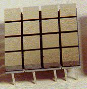
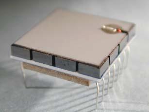
8 Let s talk about «bulk» detectors CdTe:Cl (THM) bulk detectors Ex : ISGRI (Lebrun et al.), Tokamak (Peysson et al.) CdZnTe (HPB) bulk detectors Ex : the PEGASE camera (Mestais et al.) CdTe:Cl Schottky detectors Ex : Takahashi et al. CdZnTe bulk detectors with other electrodes configurations Ex : Luke et al., Parnham et al. (ev-products) CdZnTe bulk detectors with capacitive electrodes Ex. of application : next talk (Lebrun)
9 Signal induction in a coplanar device γ-ray Photon -100 V 2 mm h + e - Q t U 0 Q 0 E γ
10 Signal induction in a coplanar device Schockley-Ramo theorem gives the instantaneous induced current I(t) If the detector is uniform, no space charge E = V 0 /L E = 1/L W The induced charge dq L at the anode is dq L = I(t) dt = q 0 dx L The induced charge is proportional to the charge carrier motion and depends on the penetration depth of the photon
11 Charge loss and balistic deficit 10µs Collected charge 1 µs 15% ~2µs 70% Charge loss (trapping) time time Balistic deficit (filtering)
12 Charge loss and balistic deficit The «collected» charge is described by the hecht relation which take into account physical trapping ie, charge transport properties (µ, τ) The hole mobility drives the rise-time, ie the balistic deficit in CdTe:Cl
13 Biparametric diagram 8 Pulse rise-time (µs) Energy (kev)
14 Charge loss correction Counts P/V 3 Pulse rise-time (µs) Energy (kev) 8000 Counts Energy (kev) P/V Energy (kev)


15 ISGRI :In Beaune 1999, we went with this

16 This time, here we are with ISGRI
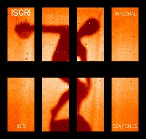

17 with spectacular images


18 Calibration phase coded mask aperture shadowgram with ISGRI camera at 511 kev The eight modules spectra with 22 Na source
 LT ~12 kev 7,5% 0 20 40 60 80 100 120 140 Energy")
19 and spectra 8 Rise-time (µs) Energy (kev) LT ~12 kev 7,5% Energy (kev)
20 Spectral performances of ISGRI CdTe Resolution FWHM (%) % (3,6 kev) 7,5 % (9 kev) 14,4 kev Energy (kev) 122 kev
21 An example of application in physics In the field of continuous thermonuclear reactions control in a Tokamak (TORE SUPRA) CdTe:Cl allows the design of compact cameras for hard X-ray tomography of the bremsstrahlung emission by electrons in tokamak fusion plamas Such electrons produce Hard X-rays between 20 and 200 kev Analyse of these electrons provides information about current density profiles Example from Peysson et al., NIMA 458, 2001, p 269
22 An example of application in physics Two cameras with 24 and 38 CdTe detectors (5 5 2 mm 3 ) Detectors stayed stable even under high fast neutrons flux and high magnetic field environment Example from Peysson et al., NIMA 458, 2001, p 269


23 PEGASE : a CZT camera for medecine Pegase is based on thick bulk CdZnTe crystals In this configuration hole signal is negligeable The associated electronics (ASIC) deals with electron pulse rise-time Example from Mestais et al., NIMA 458, 2001, p 62


24 PEGASE : electron loss correction All events in this window are affected to the 140 kev line of 99m Tc source 140 kev line of 99m Tc source 70% efficiency at 122 kev in a ±6.5 % window Example from Mestais et al., NIMA 458, 2001, p 62 Window selection for the line
25 CdTe:Cl with Schottky In contact The basic idea is to reduce the dark current noise contribution with a Schottky anode contact For thin detectors, it provides very nice spectra, NO BALISTIC DEFICIT The main problem is due to polarization effect. This can be solved by : - High bias voltage values - Negative temperature down to 40 C - Pusing the HV
26 CdTe:Cl close to Ge Needs a very low noise preamplifier! This often goes in the wrong direction if we must consider power consumption. FWHM 830 ev!! mm 3 Schottky CdTe diode, 1400V, -40 C Example from Takahashi et al., NIMA 1999 & IEEE TNS 2001
27 Modifying weighting potentiel on CZT The idea is to reduce the influence of the penetration depth in the signal induction modifying the weighting potential Another point is to forget the holes, ie to have a single carrier collection Then, it gives the opportunity to use thick CZT detectors - electrode configuration (ex : Parnham et al., Luke et al.) - capacitive electrodes (ex : Montemont et al.)
 Scheme from Montemont, thesis université J.")
28 Weighting potentiel in coplanar device Depth (mm) Depth (mm) Radius (mm) (mm) anode anode cathode cathode CAPture geometry, Parnham et al. from ev-products (USA) Scheme from Montemont, thesis université J. Fourier, Grenoble, 2000
29 ev-product Design : spectra Results with CAPture : -<3keV at 59.5keV, - <5 kev at kev and - <13 kev at 662 kev -reductions in low energy tailing CAPture geometry, Parnham et al. from ev-products (USA) mm 3 CZT detector Data from Parnham et al., SPIE conference, july 1999


30 CZT coplanar-grid array Coplanar-grid electrode pattern with edge compensation Substracting the signals from the two grids removes the hole contribution Data from Luke et al., NIMA 458, 2001, p cm 3 coplanar-grid electrode CZT coupled to its electronics A small voltage is applied between the two grids. Electrons are collected on one grid.

31 Capacitive electrodes CZT Depth (mm) Radius (mm) anode cathode Dielectric film screen Capacitive electrode geometry, Montemomt et al. from CEA/LETI Data from Montemont et al., IEEE TNS, 2001; VOL 48; PART 3; PART 1, p 278
32 Capacitive electrodes CZT performances mm 3 Schottky CdTe diode, 400V, 21 C NEW TREND! Energy (kev) Performance should not depend on the detector thicness
33 Bulk detectors in two words detector FWHM FWHM Thickness type [kev] at 122 kev [kev] at 662 kev [mm] CdTe CdTe Schottky 1.5 NA 0.5 CZT bulk 6? 6 CZT Capture CZT coplanar-grid CZT capacitive electrode
34 Let s talk about «pixel» arrays Fine pixel arrays Ex : - CdTe Medipix evolution (Manach et al.) - Infocµs (Stahle et al.) Medium size pixel arrays Ex : HEFT (Ramsey, Bolotnikov, Cook et al.) Small pixel effect in CdTe arrays Thick CdZnTe pixel arrays Ex : Simbol_X
35 Medipix arrays characteristics European collaboration with CERN The goal is to realize an highly integrated chip (CMOS 0.25 µm) for high count rate Xand γ-rays counting imagers with semiconductor detectors First generation (Medipix 1) developped for GaAs detectors. Readout of the hole signal New generation (Medipix 2) developped for electron collection and allows the use of CdTe semiconductor Data from Manach et al., CEA/DRT/LIST and Amendiola et al., NIMA 422, 1999, p 201
 Readout cell 55µm 55µm Data from Manach et al., CEA/DRT/LIST and Amendiola et al.")
36 Medipix arrays design Semiconductor detector Indium bump interconnexions Medipix2 readout chip ( pixels) Readout cell 55µm 55µm Data from Manach et al., CEA/DRT/LIST and Amendiola et al., NIMA 422, 1999, p 201
37 Infocµs CZT pixel arrays In the field of hard X-rays and γ-rays astronomy Focal plane for new focussing optics in the range of kev with grazing incidence mirrors This technic allows a very high spatial resolution The detector is made of a mm 2 CZT crystal, 2 mm thick. It is a pixels array. Data from Stahle et al., NIMA 436, 1999, p 138 and
 109 Cd source spectrum with Infocµs CZT detector Data from Stahle")
38 Infocµs CZT pixel arrays Counts 2.3 kev FWHM Infocµs CZT detector assembly Energy (kev) 109 Cd source spectrum with Infocµs CZT detector Data from Stahle et al., NIMA 436, 1999, p 138 and
39 HEFT CZT pixel arrays In the field of hard X-rays and γ-rays astronomy again Focal plane for the High Energy Focussing Telescope The goal of this work is to achieve less than 1 kev at 60 kev (very low noise ASIC) The detector is made of an 8 8 pixels array ( mm 3 ) with µm pixel size. Data from Ramsey, Bolotnikov, Cook et al.
 0.9 kev FWHM at 60 kev, 5 C (b) 1.1 kev FWHM at 60 kev, room temperature")
40 HEFT CZT pixel arrays HEFT CZT detector assembly Energy (kev) 241 Am spectra (a) 0.9 kev FWHM at 60 kev, 5 C (b) 1.1 kev FWHM at 60 kev, room temperature
41 Small pixel effect These nice results are possible because of the crystal quality, the ASIC performances and also the small pixel effect Small pixel effect is due to the weighting field distribution close the anode when the pixel size is less than a quarter of the thickness The nature works fine! Data from Eskin et al., Hage-Ali et al.


42 Thick CZT detectors arrays NEW TREND! 64 pixels CZT arrays, 6 mm thick
43 Conclusions Thanks to CdTe detectors, it is now possible to dream of high spectral performances, high spatial resolution and high efficiency simultaneously The high spectral resolution obliges to think about new geometries and high performance electronics Among these new geometries, capacitive electrodes detectors for bulk detectors and thick pixel arrays appear as major new trends
Development of High-Z Semiconductor Detectors and Their Applications to X-ray/gamma-ray Astronomy
 Development of High-Z Semiconductor Detectors and Their Applications to X-ray/gamma-ray Astronomy Taka Tanaka (SLAC/KIPAC) 9/19/2007 SLAC Advanced Instrumentation Seminar Outline Introduction CdTe Diode
Advances in Compound Semiconductor Radiation Detectors. a review of recent progress
 Advances in Compound Semiconductor Radiation Detectors a review of recent progress P.J. Sellin Radiation Imaging Group Department of Physics University of Surrey CZT/CdTe Review of recent developments
PERFORMANCE IMPROVEMENT OF CZT DETECTORS BY LINE ELECTRODE GEOMETRY
 Applications of Nuclear Techniques (CRETE3) International Journal of Modern Physics: Conference Series Vol. 27 (24) 4644 (8 pages) The Authors DOI:.42/S294546446 PERFORMANCE IMPROVEMENT OF CZT DETECTORS
New perspectives in X-ray detection of concealed illicit materials brought by CdTe/CdZnTe spectrometric detectors
 New perspectives in X-ray detection of concealed illicit materials brought by CdTe/CdZnTe spectrometric detectors Jean-Marc Dinten, Jean-Louis Amans, Loïck Verger, Olivier Peyret CEA-LETI, MINATEC, Recherche
THE spectroscopic performance of large volume CdZnTe
 3098 IEEE TRANSACTIONS ON NUCLEAR SCIENCE, VOL. 51, NO. 6, DECEMBER 2004 Analysis of Detector Response Using 3-D Position-Sensitive CZT Gamma-Ray Spectrometers Feng Zhang, Student Member, IEEE, Zhong He,
Semiconductor X-Ray Detectors. Tobias Eggert Ketek GmbH
 Semiconductor X-Ray Detectors Tobias Eggert Ketek GmbH Semiconductor X-Ray Detectors Part A Principles of Semiconductor Detectors 1. Basic Principles 2. Typical Applications 3. Planar Technology 4. Read-out
Semi conductor detectors for soft gamma-ray astrophysics
 Semi conductor detectors for soft gamma-ray astrophysics François Lebrun APC (UMR 7164), CEA-Saclay ISGRI PI IWORID 2005 Grenoble High-energy astronomy specific telescopes X-rays and gamma rays radio,
Development and characterization of 3D semiconductor X-rays detectors for medical imaging
 Development and characterization of 3D semiconductor X-rays detectors for medical imaging Marie-Laure Avenel, Eric Gros d Aillon CEA-LETI, DETectors Laboratory marie-laure.avenel@cea.fr Outlines Problematic
EE 5344 Introduction to MEMS CHAPTER 5 Radiation Sensors
 EE 5344 Introduction to MEMS CHAPTER 5 Radiation Sensors 5. Radiation Microsensors Radiation µ-sensors convert incident radiant signals into standard electrical out put signals. Radiant Signals Classification
Measurement of material uniformity using 3-D position sensitive CdZnTe gamma-ray spectrometers
 Nuclear Instruments and Methods in Physics Research A 441 (2000) 459}467 Measurement of material uniformity using 3-D position sensitive CdZnTe gamma-ray spectrometers Z. He *, W.Li, G.F. Knoll, D.K. Wehe,
Efficiency and Attenuation in CdTe Detectors
 Efficiency and Attenuation in CdTe Detectors Amptek Inc. Bob Redus, May 5, 00 Amptek s XR-00T-CdTe is a high performance x-ray and gamma ray detector system. Like Amptek s other XR00 products, a detector
Spatial resolved efficiency determination of CdZnTe semiconductor detectors with a collimated gamma-ray source for the C0BRA experiment
 Institute of Nuclear and Particle Physics, Prof. K. Zuber Spatial resolved efficiency determination of CdZnTe semiconductor detectors with a collimated gamma-ray source for the C0BRA experiment Arnd Sörensen
Polaris 3-D CdZnTe (CZT) Gamma-Ray Imaging Spectrometers
 Gamma-Ray Imaging Spectrometers") Polaris 3-D CdZnTe (CZT) Gamma-Ray Imaging Spectrometers Zhong He ISOE-ALARA Symposium, January 12, 2015 Acknowledgements: DOD, DOE and DHS John M. Palms Outstanding Innovation Began in early 1960s Thank
Polaris 3-D CdZnTe (CZT) Gamma-Ray Imaging Spectrometers Zhong He ISOE-ALARA Symposium, January 12, 2015 Acknowledgements: DOD, DOE and DHS John M. Palms Outstanding Innovation Began in early 1960s Thank
Semiconductor Detectors
 Radiation Measurement Systems Semiconductor Detectors Ho Kyung Kim Pusan National University Semiconductors Differences btwn semiconductor & gas as a material for radiation detectors Higher (1,000 ) Free
Application of Nuclear Physics
 Application of Nuclear Physics Frontier of gamma-ray spectroscopy 0.1 IR visible light UV soft X-ray X-ray hard X-ray gamma-ray 1 10 100 1e3 1e4 1e5 1e6 energy [ev] Photoelectric effect e - Compton scattering
Development of Gamma-ray Monitor using CdZnTe Semiconductor Detector
 Development of Gamma-ray Monitor using CdZnTe Semiconductor Detector A. H. D. Rasolonjatovo 1, T. Shiomi 1, T. Nakamura 1 Y. Tsudaka 2, H. Fujiwara 2, H. Araki 2, K. Matsuo 2, H. Nishizawa 2 1 Cyclotron
ORIGAMIX, A CDTE-BASED SPECTRO-IMAGER DEVELOPMENT FOR NUCLEAR APPLICATIONS
 ORIGAMIX, A CDTE-BASED SPECTRO-IMAGER DEVELOPMENT FOR NUCLEAR APPLICATIONS Sébastien Dubos 1 Hermine Lemaire 2 Frédérick Carrel 2 Olivier Limousin 1 Aline Meuris 1 Stéphane Schanne 1 Vincent Schoepff 2
Development of a Spectral Model Based on Charge Transport for the Swift/BAT 32K CdZnTe Detector Array
 Development of a Spectral Model Based on Charge Transport for the Swift/BAT 32K CdZnTe Detector Array Goro Sato a,b, Ann Parsons c Derek Hullinger c,d Masaya Suzuki e Tadayuki Takahashi a,b Makoto Tashiro
High-Resolution Gamma-Ray and Neutron Detectors For Nuclear Spectroscopy
 High-Resolution Gamma-Ray and Neutron Detectors For Nuclear Spectroscopy Thomas Niedermayr, I. D. Hau, S. Terracol, T. Miyazaki, S. E. Labov and S. Friedrich Former colleagues: M. F. Cunningham, J. N.
ISPA-Tubes with YAP:Ce Active Windows for X and Gamma Ray Imaging.
 PIXEL 2000 International Workshop on Semiconductor Pixel Detectors for Particles and X-Rays Genova - Porto Antico - Magazzini del Cotone (Sala Libeccio) June 5-8, 2000 ISPA-Tubes with YAP:Ce Active Windows
Development of semiconductor imaging detectors for a Si/CdTe Compton camera
 SLAC-PUB-12926 October 27 Development of semiconductor imaging detectors for a Si/CdTe Compton camera Shin Watanabe a,, Shin ichiro Takeda a,b, Shin-nosuke Ishikawa a,b, Hirokazu Odaka a,b, Masayoshi Ushio
Application Note ANCZT-2 Rev. 3 Charge Trapping in XR-100T-CdTe and -CZT Detectors
 Application Note ANCZT-2 Rev. 3 Charge Trapping in XR-1T-CdTe and -CZT Detectors Robert Redus, November 27 ANCZT-2 Rev 3 The XR-1T-CdTe and CdTe-Stack detectors are high performance X-ray and γ-ray detection
Results of a Si/CdTe Compton Telescope
 Results of a Si/CdTe Compton Telescope Kousuke Oonuki a,b, Takaaki Tanaka a,b, Shin Watanabe a, Shin ichiro Takeda a,b, Kazuhiro Nakazawa a, Takefumi Mitani a,b, Tadayuki Takahashi a,b, Hiroyasu Tajima
Hard X- and g-ray measurements with a large volume coplanar grid CdZnTe detector
 Nuclear Instruments and Methods in Physics Research A 563 (26) 242 248 www.elsevier.com/locate/nima Hard X- and g-ray measurements with a large volume coplanar grid CdZnTe detector Alan Owens a,, T. Buslaps
Advantages / Disadvantages of semiconductor detectors
 Advantages / Disadvantages of semiconductor detectors Semiconductor detectors have a high density (compared to gas detector) large energy loss in a short distance diffusion effect is smaller than in gas
Cadmium Zinc Telluride (CZT) Detectors
 Detectors") Cadmium Zinc Telluride (CZT) Detectors Lee Sobotka (Presenter: Walter Reviol) Oak Ridge, March 2003 WHY: Small portable/mateable device primarily for fast-beam spectrosc. CZT 1) Effective Z ~ 50 PE(dominates
Cadmium Zinc Telluride (CZT) Detectors Lee Sobotka (Presenter: Walter Reviol) Oak Ridge, March 2003 WHY: Small portable/mateable device primarily for fast-beam spectrosc. CZT 1) Effective Z ~ 50 PE(dominates
Silicon Drift Detectors for gamma-ray detection: 15 years of research (and collaboration between Politecnico and INAF-Milano)
") Silicon Drift Detectors for gamma-ray detection: 15 years of research (and collaboration between Politecnico and INAF-Milano) Outline The Silicon Drift Detector (SDD) Gamma-ray detectors based on scintillators
Silicon Drift Detectors for gamma-ray detection: 15 years of research (and collaboration between Politecnico and INAF-Milano) Outline The Silicon Drift Detector (SDD) Gamma-ray detectors based on scintillators
THE mobility-lifetime product (μτ) is used to characterize
 is used to characterize") 1832 IEEE TRANSACTIONS ON NUCLEAR SCIENCE, VOL. 63, NO. 3, JUNE 2016 A Correction Factor to the Two-Bias Method for Determining Mobility-Lifetime Products in Pixelated Detectors Will Koehler, Michael Streicher,
1832 IEEE TRANSACTIONS ON NUCLEAR SCIENCE, VOL. 63, NO. 3, JUNE 2016 A Correction Factor to the Two-Bias Method for Determining Mobility-Lifetime Products in Pixelated Detectors Will Koehler, Michael Streicher,
Recent Advances on CdTe/CdZnTe detectors
 Recent Advances on CdTe/CdZnTe detectors For High Energy PHOTON Tad Takahashi Institute of Space and Astronautical Science (ISAS) Japan Aerospace exploration Agency (JAXA) and Univ. of Tokyo Acknowledgement
Classification of Solids
 Classification of Solids Classification by conductivity, which is related to the band structure: (Filled bands are shown dark; D(E) = Density of states) Class Electron Density Density of States D(E) Examples
arxiv:astro-ph/ v1 6 Mar 2001
 Investigation of charge sharing among electrode strips for a CdZnTe detector E. Kalemci a,1 J. L. Matteson a arxiv:astro-ph/0103097v1 6 Mar 2001 Abstract a Center for Astrophysics and Space Sciences, University
Detector R&D at KIPAC. Hiro Tajima Kavli InStitute of Particle Astrophysics and Cosmology
 Detector R&D at KIPAC Hiro Tajima Kavli InStitute of Particle Astrophysics and Cosmology Detector R&D Overview Si detector ASIC Integration GLAST GeV Gamma-ray Observatory ASIC DAQ Next generation X-ray
Outline. Introduction, motivation Readout electronics, Peltier cooling Input J-FETsJ
 Progress in low energy X-rayX spectroscopy using semi-insulating insulating GaAs detectors F. Dubecký 1, B. Zaťko 1, P. Boháček 1, L. Ryć 2, E. Gombia 2, and V. Nečas 3 1 IEE SAS, Bratislava, Slovakia
Nuclear Instruments and Methods in Physics Research A
 Nuclear Instruments and Methods in Physics Research A 671 (2012) 1 5 Contents lists available at SciVerse ScienceDirect Nuclear Instruments and Methods in Physics Research A journal homepage: www.elsevier.com/locate/nima
Compton Camera. Compton Camera
 Diagnostic Imaging II Student Project Compton Camera Ting-Tung Chang Introduction The Compton camera operates by exploiting the Compton Effect. It uses the kinematics of Compton scattering to contract
SENSITIVITY ANALYSIS TO EVALUATE THE TRANSPORT PROPERTIES OF CdZnTe DETECTORS USING ALPHA PARTICLES AND LOW-ENERGY GAMMA-RAYS
 http://dx.doi.org/10.5516/net.2011.43.6.567 SENSITIVITY ANALYSIS TO EVALUATE THE TRANSPORT PROPERTIES OF CdZnTe DETECTORS USING ALPHA PARTICLES AND LOW-ENERGY GAMMA-RAYS KYUNG-O KIM 1, WOO SANG AHN 2,
Review of the Shockley Ramo theorem and its application in semiconductor gamma-ray detectors
 Nuclear Instruments and Methods in Physics Research A 463 (2001) 250 267 Review of the Shockley Ramo theorem and its application in semiconductor gamma-ray detectors Zhong He* Department of Nuclear Engineering
Detecting high energy photons. Interactions of photons with matter Properties of detectors (with examples)
") Detecting high energy photons Interactions of photons with matter Properties of detectors (with examples) Interactions of high energy photons with matter Cross section/attenution length/optical depth Photoelectric
Detecting high energy photons Interactions of photons with matter Properties of detectors (with examples) Interactions of high energy photons with matter Cross section/attenution length/optical depth Photoelectric
EEE4106Z Radiation Interactions & Detection
 EEE4106Z Radiation Interactions & Detection 2. Radiation Detection Dr. Steve Peterson 5.14 RW James Department of Physics University of Cape Town steve.peterson@uct.ac.za May 06, 2015 EEE4106Z :: Radiation
Radioactivity. Lecture 6 Detectors and Instrumentation
 Radioactivity Lecture 6 Detectors and Instrumentation The human organs Neither humans nor animals have an organ for detecting radiation from radioactive decay! We can not hear it, smell it, feel it or
CADMIUM telluride (CdTe) and cadmium zinc telluride
 and cadmium zinc telluride") IEEE TRANSACTIONS ON NUCLEAR SCIENCE, VOL. XX, NO. Y, MONTH 2001 100 CdTe stacked detectors for Gamma-ray detection Shin Watanabe, Tadayuki Takahashi, Yuu Okada, Goro Sato, Manabu Kouda, Takefumi Mitani,
IEEE TRANSACTIONS ON NUCLEAR SCIENCE, VOL. XX, NO. Y, MONTH 2001 100 CdTe stacked detectors for Gamma-ray detection Shin Watanabe, Tadayuki Takahashi, Yuu Okada, Goro Sato, Manabu Kouda, Takefumi Mitani,
Silicon Detectors in High Energy Physics
 Thomas Bergauer (HEPHY Vienna) IPM Teheran 22 May 2011 Sunday: Schedule Silicon Detectors in Semiconductor Basics (45 ) Detector concepts: Pixels and Strips (45 ) Coffee Break Strip Detector Performance
X- & γ-ray Instrumentation
 X- & γ-ray Instrumentation Used nuclear physics detectors Proportional Counters Scintillators The Dark Ages Simple collimators HEAO A1 & A2: 2 x 8 degree field of view Confusion limit is about 200 sources
Review of Semiconductor Drift Detectors
 Pavia October 25, 2004 Review of Semiconductor Drift Detectors Talk given by Pavel Rehak following a presentation on 5 th Hiroshima Symposium of Semiconductor Tracking Detectors Outline of the Review Principles
Investigation of the Asymmetric Characteristics and Temperature Effects of CdZnTe Detectors
 2068 IEEE TRANSACTIONS ON NUCLEAR SCIENCE, VOL. 52, NO. 5, OCTOBER 2005 Investigation of the Asymmetric Characteristics and Temperature Effects of CdZnTe Detectors Benjamin W. Sturm, Student Member, IEEE,
PROJECT STATUS AND PERSPECTIVES
 COBRA CdZnTe 0-NEUTRINO BETA-BETA RESEARCH APPARATUS PROJECT STATUS AND PERSPECTIVES DATE JULY 28, 2011 BY JERRAD MARTIN Agenda Introduction to COBRA Past Results Status of Current R&D PROJECT STATUS AND
Hard Xray Diagnostic for Lower Hybrid Current Drive on Alcator C- Mod
 Hard Xray Diagnostic for Lower Hybrid Current Drive on Alcator C- Mod J. Liptac, J. Decker, R. Parker, V. Tang, P. Bonoli MIT PSFC Y. Peysson CEA Cadarache APS 3 Albuquerque, NM Abstract A Lower Hybrid
Photonic Communications Engineering Lecture. Dr. Demetris Geddis Department of Engineering Norfolk State University
 Photonic Communications Engineering Lecture Dr. Demetris Geddis Department of Engineering Norfolk State University Light Detectors How does this detector work? Image from visionweb.com Responds to range
Semiconductor Detectors
 Semiconductor Detectors Summary of Last Lecture Band structure in Solids: Conduction band Conduction band thermal conductivity: E g > 5 ev Valence band Insulator Charge carrier in conductor: e - Charge
The Best Gamma-Ray Detector
 /sec The Best Gamma-Ray Detector What is the best detector for gamma-ray spectroscopy? Amptek, Inc. provides signal processing electronics which can be used with a variety of detectors (some available
SUPPLEMENTARY INFORMATION
 In the format provided by the authors and unedited. DOI: 1.138/NMAT4927 Dopant Compensation in Alloyed CH 3 NH 3 PbBr 3-x Cl x Perovskite Single Crystals for Gamma-ray Spectroscopy Haotong Wei 1, Dylan
Position Sensitive Germanium Detectors for the Advanced Compton Telescope
 Position Sensitive Germanium Detectors for the Advanced Compton Telescope R.A. Kroeger 1, W.N. Johnson 1, J.D. Kurfess 1, B.F. Phlips, P.N. Luke 3, M. Momayezi 4, W.K. Warburton 4 1 Naval Research Laboratory,
Gamma-ray Spectroscopy with LaBr 3 :Ce Scintillator Readout by a Silicon Drift Detector
 Gamma-ray Spectroscopy with LaBr 3 :Ce Scintillator Readout by a Silicon Drift Detector C. Fiorini, member, IEEE, A. Gola, M. Zanchi, A. Longoni, P. Lechner, H. Soltau, L. Strüder Abstract In this work
Stability and Characteristics of Large CZT Coplanar Electrode Detectors
 272 IEEE TRANSACTIONS ON NUCLEAR SCIENCE, VOL. 48, NO. 3, JUNE 2001 Stability and Characteristics of Large CZT Coplanar Electrode Detectors José M. Pérez, Zhong He, Senior Member, IEEE, and David K. Wehe,
A CdTe detector with a Gd converter for thermal neutron detection
 A CdTe detector with a Gd converter for thermal neutron detection Aki Miyake, Takahiro Nishika, Shailendra Singh, Hisashi Morii, Hidenori Minura, Toru Aoki. Nuclear Instruments and Methods in Physics Research
Final report on DOE project number DE-FG07-99ID High Pressure Xenon Gamma-Ray Spectrometers for Field Use
 Final report on DOE project number DE-FG07-99ID13772 High Pressure Xenon Gamma-Ray Spectrometers for Field Use Principle Investigator: Glenn K. Knoll Co-investigator: David K. Wehe, Zhong He, University
Lecture 2. Introduction to semiconductors Structures and characteristics in semiconductors
 Lecture 2 Introduction to semiconductors Structures and characteristics in semiconductors Semiconductor p-n junction Metal Oxide Silicon structure Semiconductor contact Literature Glen F. Knoll, Radiation
Neutron Induced Nuclear Counter Effect in Hamamatsu Silicon APDs and PIN Diodes
 Neutron Induced Nuclear Counter Effect in Hamamatsu Silicon APDs and PIN Diodes Rihua Mao, Liyuan Zhang, Ren-yuan Zhu California Institute of Technology Introduction Because of its immunity to magnetic
Simulation of charge transport in pixelated CdTe
 Journal of Instrumentation OPEN ACCESS Simulation of charge transport in pixelated CdTe To cite this article: M Kolstein et al View the article online for updates and enhancements. Related content - Evaluation
Photon Instrumentation. First Mexican Particle Accelerator School Guanajuato Oct 6, 2011
 Photon Instrumentation First Mexican Particle Accelerator School Guanajuato Oct 6, 2011 Outline The Electromagnetic Spectrum Photon Detection Interaction of Photons with Matter Photoelectric Effect Compton
Detection of X-Rays. Solid state detectors Proportional counters Microcalorimeters Detector characteristics
 Detection of X-Rays Solid state detectors Proportional counters Microcalorimeters Detector characteristics Solid State X-ray Detectors X-ray interacts in material to produce photoelectrons which are collected
CVD Diamond History Introduction to DDL Properties of Diamond DDL Proprietary Contact Technology Detector Applications BDD Sensors
 Diamond Detectors CVD Diamond History Introduction to DDL Properties of Diamond DDL Proprietary Contact Technology Detector Applications BDD Sensors Kevin Oliver CEO Alex Brown Sales & Marketing 20 May,
Mass Determination of Rn and Hg isotopes using MASHA
 Mass Determination of Rn and Hg isotopes using MASHA Alfred M. Sehone Lumkile Msebi Oleg Lishyk Stanislav Stanishevski Yuliya Brechko Supervisor Krupa Lubosh Flerov Laboratory of Nuclear reactions, JINR,
Status and Perspectives of the COBRA-Experiment
 Status and Perspectives of the COBRA-Experiment Jan Tebrügge for the COBRA Collaboration Status and Perspectives of the COBRA-Experiment Jan Tebrügge beta decays for thedouble COBRA Collaboration CdZnTe
Chemical Engineering 412
 Chemical Engineering 412 Introductory Nuclear Engineering Lecture 26 Radiation Detection & Measurement II Spiritual Thought 2 I would not hold the position in the Church I hold today had I not followed
Soft Gamma-ray Detector (SGD) for the NeXT mission and beyond Astro-E2 Tadayuki Takahashi
 for the NeXT mission and beyond Astro-E2 Tadayuki Takahashi") T.Takahashi, Astronomy with Radioactivies IV,2003 Soft Gamma-ray Detector (SGD) for the NeXT mission and beyond Astro-E2 Tadayuki Takahashi Institute of Space and Astronautical Science (ISAS, Japan) 2005
T.Takahashi, Astronomy with Radioactivies IV,2003 Soft Gamma-ray Detector (SGD) for the NeXT mission and beyond Astro-E2 Tadayuki Takahashi Institute of Space and Astronautical Science (ISAS, Japan) 2005
Lecture 2. Introduction to semiconductors Structures and characteristics in semiconductors
 Lecture 2 Introduction to semiconductors Structures and characteristics in semiconductors Semiconductor p-n junction Metal Oxide Silicon structure Semiconductor contact Literature Glen F. Knoll, Radiation
arxiv: v2 [physics.ins-det] 8 Feb 2013
![arxiv: v2 [physics.ins-det] 8 Feb 2013](/thumbs/91/107598870.jpg "arxiv: v2 [physics.ins-det] 8 Feb 2013") Preprint typeset in JINST style - HYPER VERSION arxiv:1302.0278v2 [physics.ins-det] 8 Feb 2013 Investigation of gamma ray detection performance of thin LFS scintillator with MAPD readout E.Guliyev a, F.Ahmadov
Preprint typeset in JINST style - HYPER VERSION arxiv:1302.0278v2 [physics.ins-det] 8 Feb 2013 Investigation of gamma ray detection performance of thin LFS scintillator with MAPD readout E.Guliyev a, F.Ahmadov
Energetic particles and their detection in situ (particle detectors) Part II. George Gloeckler
 Part II. George Gloeckler") Energetic particles and their detection in situ (particle detectors) Part II George Gloeckler University of Michigan, Ann Arbor, MI University of Maryland, College Park, MD Simple particle detectors Gas-filled
Energetic particles and their detection in situ (particle detectors) Part II George Gloeckler University of Michigan, Ann Arbor, MI University of Maryland, College Park, MD Simple particle detectors Gas-filled
CALISTE and its applications
 CALISTE and its applications Daniel Maier 1, P.A. Bausson 2, C. Blondel 1, F. Carrel 3, G. Daniel 1, C. Force 3, O. Gevin 2, H. Lemaire 3, O. Limousin 1, D. Renaud 1, J. Martignac 1, A. Meuris 1, V. Schoepff
DEVELOPMENT OF ADVANCED NEUTRON INDUCED PROMPT GAMMA- RAY ANALYSIS SYSTEM FOR SURVEY OF ANTI-PERSONNEL MINES
 DEVELOPMENT OF ADVANCED NEUTRON INDUCED PROMPT GAMMA- RAY ANALYSIS SYSTEM FOR SURVEY OF ANTI-PERSONNEL MINES T. Iguchi 1, J. Kawarabayashi 1, K. Watanabe 1, K. Nishimura 2, T. Handa 2 and H. Sawamura 2
Gamma and X-Ray Detection
 Gamma and X-Ray Detection DETECTOR OVERVIEW The kinds of detectors commonly used can be categorized as: a. Gas-filled Detectors b. Scintillation Detectors c. Semiconductor Detectors The choice of a particular
Scintillation Detectors
 Scintillation Detectors J.L. Tain Jose.Luis.Tain@ific.uv.es http://ific.uv.es/gamma/ Instituto de Física Corpuscular C.S.I.C - Univ. Valencia Scintillation detector: SCINTILLATION MATERIAL LIGHT-GUIDE
Detector R&D in KAPAC
 Detector R&D in KAPAC Hiroyasu Tajima Stanford Linear Accelerator Center Kavli Institute for Particle Astrophysics and Cosmology Outline Compton Camera SOI detector Scintillator Polarimeter Cherenkov Camera
Solid State Detectors
 Solid State Detectors Most material is taken from lectures by Michael Moll/CERN and Daniela Bortoletto/Purdue and the book Semiconductor Radiation Detectors by Gerhard Lutz. In gaseous detectors, a charged
A NEW GENERATION OF GAMMA-RAY TELESCOPE
 A NEW GENERATION OF GAMMA-RAY TELESCOPE Aleksandar GOSTOJIĆ CSNSM, Orsay, France 11 th Russbach School on Nuclear Astrophysics, March 2014. Introduction: Gamma-ray instruments GROUND BASED: ENERGY HIGHER
Lecture 18. New gas detectors Solid state trackers
 Lecture 18 New gas detectors Solid state trackers Time projection Chamber Full 3-D track reconstruction x-y from wires and segmented cathode of MWPC z from drift time de/dx information (extra) Drift over
Estimate of Large CZT Detector Absolute Efficiency
 2010 IEEE TRANSACTIONS ON NUCLEAR SCIENCE, VOL. 49, NO. 4, AUGUST 2002 Estimate of Large CZT Detector Absolute Efficiency J. M. Pérez, Member, IEEE,Z.He, Senior Member, IEEE, D.K.Wehe, Senior Member, IEEE,
Detectors for High Resolution Gamma-ray Imaging Based on a Single CsI(Tl) Scintillator Coupled to an Array of Silicon Drift Detectors
 Scintillator Coupled to an Array of Silicon Drift Detectors") 1 Detectors for High Resolution Gamma-ray Imaging Based on a Single CsI(Tl) Scintillator Coupled to an Array of Silicon Drift Detectors C. Fiorini, A. Longoni, F. Perotti, C. Labanti, E. Rossi, P. Lechner,
1 Detectors for High Resolution Gamma-ray Imaging Based on a Single CsI(Tl) Scintillator Coupled to an Array of Silicon Drift Detectors C. Fiorini, A. Longoni, F. Perotti, C. Labanti, E. Rossi, P. Lechner,
detector development Matthias Beilicke X ray Science Analysis Group meeting (12 April 2013, Monterey, CA) Collaborators: GSFC, BNL
 Collaborators: GSFC, BNL") X-ray X-ray detector detector development development at at Washington Washington University University in in St.Louis St.Louis Matthias Beilicke Washington University in St.Louis, Physics Department &
X-ray X-ray detector detector development development at at Washington Washington University University in in St.Louis St.Louis Matthias Beilicke Washington University in St.Louis, Physics Department &
Semiconductor-Detectors
 Semiconductor-Detectors 1 Motivation ~ 195: Discovery that pn-- junctions can be used to detect particles. Semiconductor detectors used for energy measurements ( Germanium) Since ~ 3 years: Semiconductor
Nuclear Instruments and Methods in Physics Research A
 Nuclear Instruments and Methods in Physics Research A 683 (2012) 53 62 Contents lists available at SciVerse ScienceDirect Nuclear Instruments and Methods in Physics Research A journal homepage: www.elsevier.com/locate/nima
Peter Fischer, ziti, Universität Heidelberg. Silicon Detectors & Readout Electronics
 Silicon Detectors and Readout Electronics Peter Fischer, ziti, Universität Heidelberg 1 Content of the Lecture (sorted by subject) Introduction: Applications of silicon detectors Requirements, measured
arxiv: v1 [astro-ph.im] 20 May 2018
![arxiv: v1 [astro-ph.im] 20 May 2018](/thumbs/86/93296535.jpg "arxiv: v1 [astro-ph.im] 20 May 2018") Imaging and spectral performance of CdTe double-sided strip detectors for the Hard X-ray Imager onboard ASTRO-H arxiv:185.777v1 [astro-ph.im] 2 May 218 Kouichi Hagino ab, Hirokazu Odaka a, Goro Sato a,
Imaging and spectral performance of CdTe double-sided strip detectors for the Hard X-ray Imager onboard ASTRO-H arxiv:185.777v1 [astro-ph.im] 2 May 218 Kouichi Hagino ab, Hirokazu Odaka a, Goro Sato a,
Atmospheric Extinction
 Atmospheric Extinction Calibrating stellar photometry requires correction for loss of light passing through the atmosphere. Atmospheric Rayleigh and aerosol scattering preferentially redirects blue light
Performance of a Si PIN photodiode at low temperatures and in high magnetic fields
 Performance of a Si PIN photodiode at low temperatures and in high magnetic fields Frederik Wauters *, Ilya Kraev *, Nathal Severijns *, Sam Coeck *, Michael Tandecki *, Valentin Kozlov *, Dalibor Zákoucký
Activities at the Laboratory of the Nuclear Engineering Department of the Polytechnic University of Valencia
 7 th Workshop on European Collaboration for Higher Education and Research in Nuclear Engineering & Radiological Protection Bruxelles, Belgique 30 May - 1 June 2011 Activities at the Laboratory of the Nuclear
Instrumentation for sub-mm astronomy. Adam Woodcraft SUPA, University of Edinburgh
 Instrumentation for sub-mm astronomy Adam Woodcraft http://woodcraft.lowtemp.org SUPA, University of Edinburgh 1 2 Introduction Sub-mm astronomy 1 Astronomy at sub-mm wavelengths Between infrared and millimetre
Key words: avalanche photodiode, soft X-ray detector, scintillation γ-ray detector, imaging device PACS: 07.85;95.55.A;85.60.D
 We have studied the performance of large area avalanche photodiodes (APDs) recently developed by Hamamatsu Photonics K.K, in high-resolution X-rays and γ- rays detections. We show that reach-through APD
Detector R&D at KIPAC
 Detector R&D at KIPAC Hiro Tajima Kavli Institute for Particle Astrophysics and Cosmology 1 Detector R&D Overview Si detector ASIC Integration GLAST GeV Gamma-ray Observatory ASIC DAQ Next generation X-ray
Reference literature. (See: CHEM 2470 notes, Module 8 Textbook 6th ed., Chapters )
") September 17, 2018 Reference literature (See: CHEM 2470 notes, Module 8 Textbook 6th ed., Chapters 13-14 ) Reference.: https://slideplayer.com/slide/8354408/ Spectroscopy Usual Wavelength Type of Quantum
September 17, 2018 Reference literature (See: CHEM 2470 notes, Module 8 Textbook 6th ed., Chapters 13-14 ) Reference.: https://slideplayer.com/slide/8354408/ Spectroscopy Usual Wavelength Type of Quantum
ORIGAMIX CURRENT STATE OF A TECHNOLOGY TRANSFER PROJECT FROM SPACE GRADE HIGH ENERGY SPECTRO-IMAGER TO COMMERCIAL GRADE GAMMA CAMERA
 ORIGAMIX CURRENT STATE OF A TECHNOLOGY TRANSFER PROJECT FROM SPACE GRADE HIGH ENERGY SPECTRO-IMAGER TO COMMERCIAL GRADE GAMMA CAMERA Pierre-Anne BAUSSON CEA Saclay DRF/Irfu B. 709 p. 27 B. 141 p. 104 CEA
GAMMA-RAY IMAGING AND POLARIZATION MEASUREMENT USING 3-D POSITION-SENSITIVE CdZnTe DETECTORS
 GAMMA-RAY IMAGING AND POLARIZATION MEASUREMENT USING 3-D POSITION-SENSITIVE CdZnTe DETECTORS by Dan Xu A dissertation submitted in partial fulfillment of the requirements for the degree of Doctor of Philosophy
Charge sharing in silicon pixel detectors
 Nuclear Instruments and Methods in Physics Research A 487 (2002) 113 122 Charge sharing in silicon pixel detectors K. Mathieson a, *, M.S. Passmore b, P. Seller c, M.L. Prydderch c, V. O Shea a, R.L. Bates
Performance of high pressure Xe/TMA in GEMs for neutron and X-ray detection
 Performance of high pressure Xe/TMA in GEMs for neutron and X-ray detection R. Kreuger, C. W. E. van Eijk, Member, IEEE, F. A. F. Fraga, M. M. Fraga, S. T. G. Fetal, R. W. Hollander, Member, IEEE, L. M.
Introduction to the Diagnosis of Magnetically Confined Thermonuclear Plasma
 Introduction to the Diagnosis of Magnetically Confined Thermonuclear Plasma Core diagnostics II: Bolometry and Soft X-rays J. Arturo Alonso Laboratorio Nacional de Fusión EURATOM-CIEMAT E6 P2.10 arturo.alonso@ciemat.es
Chap. 11 Semiconductor Diodes
 Chap. 11 Semiconductor Diodes Semiconductor diodes provide the best resolution for energy measurements, silicon based devices are generally used for charged-particles, germanium for photons. Scintillators
RESPONSE CALCULATIONS OF THE CdZnTe DETECTOR USING EGS4. James C. Liu, W. R. Nelson and R. Seefred
 SLAC-PUB-8606 (September 5, 2000) RESPONSE CALCULATIONS OF THE CdZnTe DETECTOR USING EGS4 James C. Liu, W. R. Nelson and R. Seefred Stanford Linear Accelerator Center, MS 48, P. O. Box 4349, Stanford,
Maximum-Likelihood Deconvolution in the Spatial and Spatial-Energy Domain for Events With Any Number of Interactions
 IEEE TRANSACTIONS ON NUCLEAR SCIENCE, VOL. 59, NO. 2, APRIL 2012 469 Maximum-Likelihood Deconvolution in the Spatial and Spatial-Energy Domain for Events With Any Number of Interactions Weiyi Wang, Member,
Germanium Detectors. Germanium, a special material. Detectors, big is beautiful. Operational features. Applications. Iris Abt
 Germanium Detectors Germanium, a special material Detectors, big is beautiful Operational features Applications Iris Abt Si Si Si Si Si Si n silicon Si + P The Material Si Donor Si Si conduction valence