M. De Napoli, F. Giacoppo, G. Raciti, E. Rapisarda, C. Sfienti. Laboratori Nazionali del Sud (LNS) INFN University of Catania. IPRD Oct.
|
|
|
- Milo Jenkins
- 5 years ago
- Views:
Transcription
1 M. De Napoli, F. Giacoppo, G. Raciti, E. Rapisarda, C. Sfienti Laboratori Nazionali del Sud (LNS) INFN University of Catania IPRD Oct. Siena

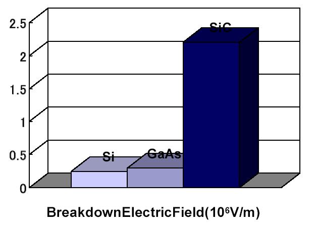
2 Silicon carbide (SiC) is expected to be applied to high-power devices. WIDE BANDGAP ->LOW LEAKAGE CURRENT HIGH SENSIVITY 100 times Radiation Hard than Si

 Schottky diodes lightning arresterss in")


3 Applications 12 Thyristors MOSFET VR=400V di/dt=400 A/µs trr=8 ns MESFET K 300 K 300 K Reverse voltage (V) Schottky diodes lightning arresterss in electric power systems Current (A) Electronic devices: Time (ns) JFET Astronomy and Aereospace: mirror material for astronomical telescopes X-Rays detectors in harsh environments Nuclear Physiscs Detectors Neutrons, protons, alphas, light ions detectors blue LEDs
4 Detection of alpha, 12C, 16O ions at different energies: Linearity Depleted region vs applied reverse bias Charge collection Energy resolution Signal rise-time Radiation Damage


5 SiC from ETC-Catania The Schottky diodes were fabricated by epitaxy onto high-purity 4H-SiC n-type substrate from the ETC - Catania Deposition temperature 1600 C Deposition rate 7 µm/hr Uniformity on wafer ±1.5%

6 Detector chips were glued on a brass foil and bonded on a board 0.5x0.5 mm2 2x2 mm2 1x1 mm2 Each chip contains 5 individual detectors of different area


7 LNS Tandem accelerator 13 MV 1 measurement st 2nd measurement C Inc. Energies: MeV 16 O : MeV 12 C Inc. Energies: MeV 16 O : 35.2 MeV 12
8 A 300 µm Si has been used for comparison The Silicon detector has been calibrated by using a one peak Am alpha source and calibrated pulser 4 Al foils have been used to provide alphas at different incident energies
9 Alpha energies 2.19 MeV (18 µm Al) 2.72 MeV (16 µm Al) 3.18 MeV (13 µm Al) 3.76 MeV (10 µm Al) Tandem beams allow to extend the energy range explored with alpha particles: 12 C at 5.04 MeV and MeV 16 O at 7.3 MeV, 9.78 MeV, MeV, MeV, MeV High degree of linearity F. Nava et al., NIM A437 (1999)354 F.H. Ruddy et al., NIM A505 (2003)159 W. Cunningham et al., NIM A 509 (2003)127
10 Black peaks refers to SiC signals calibrated according to Si calibration Sipeak/SiCpeak = 2.08
 = 7.82 +- 0.15 ev")
11 Ee-h (Si) = 3.76 ev Sipeak/SiCpeak = Ee-h (SiC) = ev
12 Incident alpha energy: 3.18 MeV According to SRIM calculation the range in SiC is 13µm Signals increase with increasing bias voltage At saturation the active area is the range of 3.18 MeV alphas in SiC (13µm)
13 Black dots: depletion measured with alpha particles Red dots: depletion measured with Tandem beams Vbuilt-in 1.3 um resulting from the Schottky contact potential F. Nava et al., NIM A437 (1999)354 d= 2ε (Vrev + Vbuilt in ) qn eff 400 Volts -> active region of 13 µm!
14 where: V Applied reverse Bias N Doping Concentration ε the static permittivity of the material ε =9.66 ε0 [24] where ε0 is the electric constant ε0 = F/m. e are the electron charge V built-in is the magnitude of the Schottky barrier 1.5 V o lts, [25]. 2nd Measurements Energy lost in the 0.2 µm Ni2-Si front layer Type Nominal doping (N/cm3 ) Thickness(µm) C Energy (MeV) 12 A B C Energy Corrected

15 SiC- type b 12 C 27.7 MeV Vbias A- Low Doping B- Medium Doping C- High Doping
16 2nd Measurements A- Low Doping B- Medium Doping 1st Measurements C- High Doping
17
18 Charge Collection Measured Depleted region
19 Charge Collection Same Lp value for the three 12C energies
20 Charge Collection Lp = 4±1µm τp = 52 ±20 ns Lp = 7±1µm τp = 160 ±40 ns Lp=((KT/e)µp τp) where: Lp < 0.5 µm 1/2 τp ho le lifetim e T temperature µp o hm ic hole m obility µp= 120 cm 2 V-1 s -1 e elec tro n c ha rg e Diffusion process negligible: probably higher density of defects
21 ENERGY RESOLUTION = 2.8% C peak = 9.26 MeV (larger than typical Si resolution) FWHM = 381 kev F.H. Ruddy et al., NIM A505 (2003) kev
22 Low Doping Concentration Medium Doping Concentration High Doping Concentration
23 C beam at MeV 12 Tektronix TDS 5104B Digital Oscilloscope
 RISE TIME (nsec) Decrease of rise time: 44 nsec Bias")
24 Drift Velocity α Vbias α 1/sqrt(Vbias) Depleted region thickness α sqrt(vbias) RISE TIME (nsec) Decrease of rise time: 44 nsec Bias (Volts)
25 Irradiated with 53 MeV 16O beam The amplitude drops to 50% Reverse current increases by a factor of ions/cm2 The noise increases by a factor of 2 S. Sciortino et al., NIM A552 (2005)138 Factor 10 harder than Si T. Quinn et al., Nuclear Science Symposium. Conference record, Vol.2, Portland,OR,USA,19-25 Oct. 2003
26 Low Doping Concentration High Doping Concentration


27

28 SiC from ETC-CATANIA Good Linearity Response: SiCpeak= 0.5 Sipeak Energy Resolution: 2.8% (Si <1%) Rise time: 44 nsec Radiation Damage: ions/cm2 50% ; 1015 ions/cm2 Inversion Factor 10 harder than Si Very high values of Bias needed!! but it depends on the N+ concentration
 Sciortino")
29 Beginning ions/cm ions/cm ions/cm2 INVERSION Same signals for 53 MeV and 12 MeV O beams (Space Charge Sign Inversion ) Sciortino et al. NIM A 552(2005)138 G. Lindström et al., NIM A466 (2001) 308 L. Bosisio et al., IEEE Trans. Nucl. Sci., 50 (1) (2003) 219


30
31 Silicon Carbide
32 Entries in Histogram MIMOSA II before and after irradiation with 200kRad X-Rays 800 Before After Irradiation Charge Collected in 4 Pixels [ADC] (c) Michael Deveaux Conclusion on Mimosa 2 after ~ 400kRad: Leakage currents increases by a factor ~5. Noise increases by some percent. Readout electronics OK. Charge collection drops by ~50% (kills the chip)
33 Where does the extracharge come from?
34 Ti Ni2Si SiO2 Ni n x1016 cm-3 n+ ~1018cm-3 Ni2Si Ohmic contact
35 Measured Qc E1 D E2 Q0 + Etot Calculated
36 Dynamical recovery Current (A) Reverse voltage (V) 400 K 300 K 300 K VR=400V di/dt=400 A/µs Time (ns) trr=8 ns

37 electrical application Astronomy Silicon carbide's hardness and rigidity make it a desirable mirror material for astronomical work lightning arresterss in electric power systems
38 17.68 MeV 12C beam spectra at increasing bias voltage
39
Epitaxial SiC Schottky barriers for radiation and particle detection
 Epitaxial SiC Schottky barriers for radiation and particle detection M. Bruzzi, M. Bucciolini, R. D'Alessandro, S. Lagomarsino, S. Pini, S. Sciortino INFN Firenze - Università di Firenze F. Nava INFN Bologna
GaN for use in harsh radiation environments
 4 th RD50 - Workshop on radiation hard semiconductor devices for very high luminosity colliders GaN for use in harsh radiation environments a (W Cunningham a, J Grant a, M Rahman a, E Gaubas b, J Vaitkus
First Results and Realization Status of a Proton Computed Radiography Device
 First Results and Realization Status of a Proton Computed Radiography Device V. Sipala for the PRIMA collaboration V.Sipalaa,b, D.LoPrestia,b, N.Randazzob, M.Bruzzid,e, D.Menichellie,d, C.Civininid, M.Bucciolinic,d,
Theory and practice of Materials Analysis for Microelectronics with a nuclear microprobe
 TUTORIAL Theory and practice of Materials Analysis for Microelectronics with a nuclear microprobe Ettore Vittone Physics Department University of Torino, Italy Ettore Vittone 1 IBIC for the functional
Development of Radiation Detectors Based on Semi-Insulating Silicon Carbide
 Development of Radiation Detectors Based on Semi-Insulating Silicon Carbide Frank H. Ruddy, Member, IEEE, John G. Seidel, Robert W. Flammang, Ranbir Singh, Member, IEEE, and John Schroeder Abstract Fast-neutron
Preliminary measurements of charge collection and DLTS analysis of p + /n junction SiC detectors and simulations of Schottky diodes
 Preliminary measurements of charge collection and DLTS analysis of p + /n junction SiC detectors and simulations of Schottky diodes F.Moscatelli, A.Scorzoni, A.Poggi, R.Nipoti DIEI and INFN Perugia and
Modeling of charge collection efficiency degradation in semiconductor devices induced by MeV ion beam irradiation
 Modeling of charge collection efficiency degradation in semiconductor devices induced by MeV ion beam irradiation Ettore Vittone Physics Department University of Torino - Italy 1 IAEA Coordinate Research
Schottky Rectifiers Zheng Yang (ERF 3017,
 ECE442 Power Semiconductor Devices and Integrated Circuits Schottky Rectifiers Zheng Yang (ERF 3017, email: yangzhen@uic.edu) Power Schottky Rectifier Structure 2 Metal-Semiconductor Contact The work function
Neutron Induced Nuclear Counter Effect in Hamamatsu Silicon APDs and PIN Diodes
 Neutron Induced Nuclear Counter Effect in Hamamatsu Silicon APDs and PIN Diodes Rihua Mao, Liyuan Zhang, Ren-yuan Zhu California Institute of Technology Introduction Because of its immunity to magnetic
Review of Semiconductor Drift Detectors
 Pavia October 25, 2004 Review of Semiconductor Drift Detectors Talk given by Pavel Rehak following a presentation on 5 th Hiroshima Symposium of Semiconductor Tracking Detectors Outline of the Review Principles
Semiconductor X-Ray Detectors. Tobias Eggert Ketek GmbH
 Semiconductor X-Ray Detectors Tobias Eggert Ketek GmbH Semiconductor X-Ray Detectors Part A Principles of Semiconductor Detectors 1. Basic Principles 2. Typical Applications 3. Planar Technology 4. Read-out
High-temperature characteristics of SiC Schottky barrier diodes related to physical phenomena
 High-temperature characteristics of SiC Schottky barrier diodes related to physical phenomena Tsuyoshi Funaki 1a), Tsunenobu Kimoto 2, and Takashi Hikihara 1 1 Kyoto University, Dept. of Electrical Eng.
Development of a Radiation Hard CMOS Monolithic Pixel Sensor
 Development of a Radiation Hard CMOS Monolithic Pixel Sensor M. Battaglia 1,2, D. Bisello 3, D. Contarato 2, P. Denes 2, D. Doering 2, P. Giubilato 2,3, T.S. Kim 2, Z. Lee 2, S. Mattiazzo 3, V. Radmilovic
Lecture 18. New gas detectors Solid state trackers
 Lecture 18 New gas detectors Solid state trackers Time projection Chamber Full 3-D track reconstruction x-y from wires and segmented cathode of MWPC z from drift time de/dx information (extra) Drift over
Semiconductor Detectors
 Semiconductor Detectors Summary of Last Lecture Band structure in Solids: Conduction band Conduction band thermal conductivity: E g > 5 ev Valence band Insulator Charge carrier in conductor: e - Charge
physics/ Sep 1997
 GLAS-PPE/97-6 28 August 1997 Department of Physics & Astronomy Experimental Particle Physics Group Kelvin Building, University of Glasgow, Glasgow, G12 8QQ, Scotland. Telephone: +44 - ()141 3398855 Fax:
Tracking Detector Material Issues for the slhc
 Tracking Detector Material Issues for the slhc Hartmut F.-W. Sadrozinski SCIPP, UC Santa Cruz, CA 95064 Hartmut F.-W. Sadrozinski, US ATLAS Upgrade Meeting Nov 10, 2005 1 Outline of the talk - Motivation
Abstract. II. THEORETICAL CONSIDERATIONS AND DETECTOR DESIGN A. 10 B Film Coatings and Efficiency I. INTRODUCTION
 A Study of the Effect of Incremental Gamma-Ray Doses and Incremental Neutron Fluences Upon the Performance of Self-Biased 10 B-Coated High-Purity Epitaxial GaAs Thermal Neutron Detectors H.K. Gersch 1,
Diamond (Radiation) Detectors Are Forever! Harris Kagan
 Detectors Are Forever! Harris Kagan") Diamond (Radiation) Detectors Are Forever! Outline of the Talk Introduction to Diamond Recent Results Applications Summary Diamond (Radiation) Detectors Are Forever! (page 1) Introduction Motivation: Tracking
Diamond (Radiation) Detectors Are Forever! Outline of the Talk Introduction to Diamond Recent Results Applications Summary Diamond (Radiation) Detectors Are Forever! (page 1) Introduction Motivation: Tracking
Lecture 2. Introduction to semiconductors Structures and characteristics in semiconductors
 Lecture 2 Introduction to semiconductors Structures and characteristics in semiconductors Semiconductor p-n junction Metal Oxide Silicon structure Semiconductor contact Literature Glen F. Knoll, Radiation
Structure of semiconductor detectors for characterization of ionizing radiation sources
 Structure of seiconductor detectors for characterization of ionizing radiation sources A. Cannavò 1, L. Tòrrisi 1, L. Calcagnò 2, A. Sciutò 3 1 Dottorato di Ricerca in Fisica, Università di Messina, V.le
1) CMOS-Sensors for vertex-detectors 2) CMOS-Sensors for X-ray imaging 3) Sensor with a 3-T-preamplifier 4) Sensor with nearly full depletion
 CMOS-Sensors for vertex-detectors 2) CMOS-Sensors for X-ray imaging 3) Sensor with a 3-T-preamplifier 4) Sensor with nearly full depletion") AD vanced MO nolithic ensors for S CMOS-sensors for energy-resolved X-ray imaging Dennis Doering, Samir Amar, Jerome Baudot², Michael Deveaux, Wojciech Dulinski², Maciej Kachel², Tomasz Hemperek³, Christian
AD vanced MO nolithic ensors for S CMOS-sensors for energy-resolved X-ray imaging Dennis Doering, Samir Amar, Jerome Baudot², Michael Deveaux, Wojciech Dulinski², Maciej Kachel², Tomasz Hemperek³, Christian
A new protocol to evaluate the charge collection efficiency degradation in semiconductor devices induced by MeV ions
 Session 12: Modification and Damage: Contribute lecture O-35 A new protocol to evaluate the charge collection efficiency degradation in semiconductor devices induced by MeV ions Ettore Vittone Physics
Advances in Compound Semiconductor Radiation Detectors. a review of recent progress
 Advances in Compound Semiconductor Radiation Detectors a review of recent progress P.J. Sellin Radiation Imaging Group Department of Physics University of Surrey CZT/CdTe Review of recent developments
Modelling of Diamond Devices with TCAD Tools
 RADFAC Day - 26 March 2015 Modelling of Diamond Devices with TCAD Tools A. Morozzi (1,2), D. Passeri (1,2), L. Servoli (2), K. Kanxheri (2), S. Lagomarsino (3), S. Sciortino (3) (1) Engineering Department
Test Simulation of Neutron Damage to Electronic Components using Accelerator Facilities
 Test Simulation of Neutron Damage to Electronic Components using Accelerator Facilities Donald King, Patrick Griffin, Ed Bielejec, William Wampler, Chuck Hembree, Kyle McDonald, Tim Sheridan, George Vizkelethy,
Lecture 8. Detectors for Ionizing Particles
 Lecture 8 Detectors for Ionizing Particles Content Introduction Overview of detector systems Sources of radiation Radioactive decay Cosmic Radiation Accelerators Interaction of Radiation with Matter General
Silicon Detectors in High Energy Physics
 Thomas Bergauer (HEPHY Vienna) IPM Teheran 22 May 2011 Sunday: Schedule Silicon Detectors in Semiconductor Basics (45 ) Detector concepts: Pixels and Strips (45 ) Coffee Break Strip Detector Performance
Chem 481 Lecture Material 3/20/09
 Chem 481 Lecture Material 3/20/09 Radiation Detection and Measurement Semiconductor Detectors The electrons in a sample of silicon are each bound to specific silicon atoms (occupy the valence band). If
Lecture 2. Introduction to semiconductors Structures and characteristics in semiconductors
 Lecture 2 Introduction to semiconductors Structures and characteristics in semiconductors Semiconductor p-n junction Metal Oxide Silicon structure Semiconductor contact Literature Glen F. Knoll, Radiation
1 Name: Student number: DEPARTMENT OF PHYSICS AND PHYSICAL OCEANOGRAPHY MEMORIAL UNIVERSITY OF NEWFOUNDLAND. Fall :00-11:00
 1 Name: DEPARTMENT OF PHYSICS AND PHYSICAL OCEANOGRAPHY MEMORIAL UNIVERSITY OF NEWFOUNDLAND Final Exam Physics 3000 December 11, 2012 Fall 2012 9:00-11:00 INSTRUCTIONS: 1. Answer all seven (7) questions.
EUROPEAN ORGANIZATION FOR NUCLEAR RESEARCH STUDIES OF THE RADIATION HARDNESS OF OXYGEN-ENRICHED SILICON DETECTORS
 EUROPEAN ORGANIZATION FOR NUCLEAR RESEARCH CERN EP/98 62 11 Juin 1998 STUDIES OF THE RADIATION HARDNESS OF OXYGEN-ENRICHED SILICON DETECTORS A. Ruzin, G. Casse 1), M. Glaser, F. Lemeilleur CERN, Geneva,
Development of High-Z Semiconductor Detectors and Their Applications to X-ray/gamma-ray Astronomy
 Development of High-Z Semiconductor Detectors and Their Applications to X-ray/gamma-ray Astronomy Taka Tanaka (SLAC/KIPAC) 9/19/2007 SLAC Advanced Instrumentation Seminar Outline Introduction CdTe Diode
Screens for low current beams
 Screens for low current beams P.Finocchiaro, L.Cosentino, A.Pappalardo INFN - Laboratori Nazionali del Sud Catania, Italy Status Workshop on 29-Apr-2010 on Scintillating - Preliminary Screen Applications
Lecture 2. Introduction to semiconductors Structures and characteristics in semiconductors. Fabrication of semiconductor sensor
 Lecture 2 Introduction to semiconductors Structures and characteristics in semiconductors Semiconductor p-n junction Metal Oxide Silicon structure Semiconductor contact Fabrication of semiconductor sensor
EE 130 Intro to MS Junctions Week 6 Notes. What is the work function? Energy to excite electron from Fermi level to the vacuum level
 EE 13 Intro to S Junctions eek 6 Notes Problem 1 hat is the work function? Energy to ecite electron from Fermi level to the vacuum level Electron affinity of 4.5eV Electron affinity of Ge 4.eV orkfunction
UNIVERSITY OF CALIFORNIA College of Engineering Department of Electrical Engineering and Computer Sciences. Professor Chenming Hu.
 UNIVERSITY OF CALIFORNIA College of Engineering Department of Electrical Engineering and Computer Sciences EECS 130 Spring 2009 Professor Chenming Hu Midterm I Name: Closed book. One sheet of notes is
Silicon Detectors. Particle Physics
 Mitglied der Helmholtz-Gemeinschaft Silicon Detectors for Particle Physics 9. August 2012 Ralf Schleichert, Institut für Kernphysik Outline Different Cameras Silicon Detectors Taking Pictures in Particle
Detectors for High Resolution Gamma-ray Imaging Based on a Single CsI(Tl) Scintillator Coupled to an Array of Silicon Drift Detectors
 Scintillator Coupled to an Array of Silicon Drift Detectors") 1 Detectors for High Resolution Gamma-ray Imaging Based on a Single CsI(Tl) Scintillator Coupled to an Array of Silicon Drift Detectors C. Fiorini, A. Longoni, F. Perotti, C. Labanti, E. Rossi, P. Lechner,
1 Detectors for High Resolution Gamma-ray Imaging Based on a Single CsI(Tl) Scintillator Coupled to an Array of Silicon Drift Detectors C. Fiorini, A. Longoni, F. Perotti, C. Labanti, E. Rossi, P. Lechner,
Current mechanisms Exam January 27, 2012
 Current mechanisms Exam January 27, 2012 There are four mechanisms that typically cause currents to flow: thermionic emission, diffusion, drift, and tunneling. Explain briefly which kind of current mechanisms
Fabrication of a 600V/20A 4H-SiC Schottky Barrier Diode
 Fabrication of a 600V/20A 4H-SiC Schottky Barrier Diode In-Ho Kang, Sang-Cheol Kim, Jung-Hyeon Moon, Wook Bahng, and Nam-Kyun Kim Power Ssemiconductor Research Center, Korea Electrotechnology Research
Characterisation of SiC by IBIC and other IBA techniques
 Nuclear Instruments and Methods in Physics Research B 188 (2002) 130 134 www.elsevier.com/locate/nimb Characterisation of SiC by IBIC and other IBA techniques M. Jaksic a, *, Z. Bosnjak a, D. Gracin a,
Advantages / Disadvantages of semiconductor detectors
 Advantages / Disadvantages of semiconductor detectors Semiconductor detectors have a high density (compared to gas detector) large energy loss in a short distance diffusion effect is smaller than in gas
IRRADIATION MEASUREMENTS ON THE 0.25 m CMOS PIXEL READOUT TEST CHIP BY A 14 MEV NEUTRON FACILITY
 ALICE/ITS 2000-24 Internal Note-ITS 19 September 2000 IRRADIATION MEASUREMENTS ON THE 0.25 m CMOS PIXEL READOUT TEST CHIP BY A 14 MEV NEUTRON FACILITY A. Badala, R. Barbera, F.Librizzi, A. Palmeri, G.
Quality Assurance. Purity control. Polycrystalline Ingots
 Quality Assurance Purity control Polycrystalline Ingots 1 Gamma Spectrometry Nuclide Identification Detection of Impurity Traces 1.1 Nuclides Notation: Atomic Mass Atomic Number Element Neutron Atomic
Alpha-particle Stopping Powers in Air and Argon
 Alpha-particle Stopping Powers in Air and Argon Mohammad QH 1* and Maghdid HA 2 1 Department of Physics, College of Science, Raparin University, Sulaimanyah, Iraqi Kurdistan, Iraq 2 Department of Physics,
Outline. Introduction, motivation Readout electronics, Peltier cooling Input J-FETsJ
 Progress in low energy X-rayX spectroscopy using semi-insulating insulating GaAs detectors F. Dubecký 1, B. Zaťko 1, P. Boháček 1, L. Ryć 2, E. Gombia 2, and V. Nečas 3 1 IEE SAS, Bratislava, Slovakia
Simulation results from double-sided and standard 3D detectors
 Simulation results from double-sided and standard 3D detectors David Pennicard, University of Glasgow Celeste Fleta, Chris Parkes, Richard Bates University of Glasgow G. Pellegrini, M. Lozano - CNM, Barcelona
Improvements in Realizing 4H-SiC Thermal Neutron Detectors
 EPJ Web of Conferences 106, 05004 (2016) DOI: 10.1051/epjconf/201610605004 C Owned by the authors, published by EDP Sciences, 2016 Improvements in Realizing 4H-SiC Thermal Neutron Detectors F. Issa 1,a,
Quiz #1 Practice Problem Set
 Name: Student Number: ELEC 3908 Physical Electronics Quiz #1 Practice Problem Set? Minutes January 22, 2016 - No aids except a non-programmable calculator - All questions must be answered - All questions
Edge termination study and fabrication of a 4H SiC junction barrier Schottky diode
 Edge termination study and fabrication of a 4H SiC junction barrier Schottky diode Chen Feng-Ping( ) a), Zhang Yu-Ming( ) a), Zhang Yi-Men( ) a), Tang Xiao-Yan( ) a), Wang Yue-Hu( ) a), and Chen Wen-Hao(
Chap. 11 Semiconductor Diodes
 Chap. 11 Semiconductor Diodes Semiconductor diodes provide the best resolution for energy measurements, silicon based devices are generally used for charged-particles, germanium for photons. Scintillators
PHYSICAL ELECTRONICS(ECE3540) CHAPTER 9 METAL SEMICONDUCTOR AND SEMICONDUCTOR HETERO-JUNCTIONS
 CHAPTER 9 METAL SEMICONDUCTOR AND SEMICONDUCTOR HETERO-JUNCTIONS") PHYSICAL ELECTRONICS(ECE3540) CHAPTER 9 METAL SEMICONDUCTOR AND SEMICONDUCTOR HETERO-JUNCTIONS Tennessee Technological University Wednesday, October 30, 013 1 Introduction Chapter 4: we considered the
PHYSICAL ELECTRONICS(ECE3540) CHAPTER 9 METAL SEMICONDUCTOR AND SEMICONDUCTOR HETERO-JUNCTIONS Tennessee Technological University Wednesday, October 30, 013 1 Introduction Chapter 4: we considered the
PHYSICAL ELECTRONICS(ECE3540) CHAPTER 9 METAL SEMICONDUCTOR AND SEMICONDUCTOR HETERO-JUNCTIONS
 CHAPTER 9 METAL SEMICONDUCTOR AND SEMICONDUCTOR HETERO-JUNCTIONS") PHYSICAL ELECTRONICS(ECE3540) CHAPTER 9 METAL SEMICONDUCTOR AND SEMICONDUCTOR HETERO-JUNCTIONS Tennessee Technological University Monday, November 11, 013 1 Introduction Chapter 4: we considered the semiconductor
PHYSICAL ELECTRONICS(ECE3540) CHAPTER 9 METAL SEMICONDUCTOR AND SEMICONDUCTOR HETERO-JUNCTIONS Tennessee Technological University Monday, November 11, 013 1 Introduction Chapter 4: we considered the semiconductor
DETECTORS. I. Charged Particle Detectors
 DETECTORS I. Charged Particle Detectors A. Scintillators B. Gas Detectors 1. Ionization Chambers 2. Proportional Counters 3. Avalanche detectors 4. Geiger-Muller counters 5. Spark detectors C. Solid State
Performance of a Si PIN photodiode at low temperatures and in high magnetic fields
 Performance of a Si PIN photodiode at low temperatures and in high magnetic fields Frederik Wauters *, Ilya Kraev *, Nathal Severijns *, Sam Coeck *, Michael Tandecki *, Valentin Kozlov *, Dalibor Zákoucký
Semiconductor-Detectors
 Semiconductor-Detectors 1 Motivation ~ 195: Discovery that pn-- junctions can be used to detect particles. Semiconductor detectors used for energy measurements ( Germanium) Since ~ 3 years: Semiconductor
8. Schottky contacts / JFETs
 Technische Universität Graz Institute of Solid State Physics 8. Schottky contacts / JFETs Nov. 21, 2018 Technische Universität Graz Institute of Solid State Physics metal - semiconductor contacts Photoelectric
Test Simulation of Neutron Damage to Electronic Components using Accelerator Facilities
 1 AP/DM-05 Test Simulation of Neutron Damage to Electronic Components using Accelerator Facilities D. King 1, E. Bielejec 1, C. Hembree 1, K. McDonald 1, R. Fleming 1, W. Wampler 1, G. Vizkelethy 1, T.
Avalanche breakdown. Impact ionization causes an avalanche of current. Occurs at low doping
 Avalanche breakdown Impact ionization causes an avalanche of current Occurs at low doping Zener tunneling Electrons tunnel from valence band to conduction band Occurs at high doping Tunneling wave decays
CTU Prague RD50 Group
 CTU Prague RD50 Group Detector structures on GaAs (Mesa with Guard Rings) T. Horazdovský, D. Chren, Z. Kohout, M. Solar, B. Sopko ME CTU V. Jurka, E. Hulicius IP ASCR S. Pospisil IEAP CTU Contents Motivation
Study of radiation damage induced by 82 MeV protons on multipixel Geiger-mode avalanche photodiodes
 Study of radiation damage induced by 82 MeV protons on multipixel Geiger-mode avalanche photodiodes Y. Musienko*, S. Reucroft, J. Swain (Northeastern University, Boston) D. Renker, K. Dieters (PSI, Villigen)
First Applications of CVD-Diamond Detectors in Heavy-ion Experiments
 First Applications of CVD-Diamond Detectors in Heavy-ion Experiments E. Berdermann*, K. Blasche, P. Moritz, H. Stelzer*, B. Voss, F. Zeytouni Gesellschaft für Schwerionenforschung (GSI), Planckstraße 1,
For the following statements, mark ( ) for true statement and (X) for wrong statement and correct it.
 for true statement and (X) for wrong statement and correct it.") Benha University Faculty of Engineering Shoubra Electrical Engineering Department First Year communications. Answer all the following questions Illustrate your answers with sketches when necessary. The
Benha University Faculty of Engineering Shoubra Electrical Engineering Department First Year communications. Answer all the following questions Illustrate your answers with sketches when necessary. The
Micro Pixel Chamber with resistive electrodes for spark reduction
 Micro Pixel Chamber with resistive electrodes for spark reduction arxiv:1310.5550v1 [physics.ins-det] 21 Oct 2013 Atsuhiko Ochi a, Yuki Edo a, Yasuhiro Homma a, Hidetoshi Komai a and Takahiro Yamaguchi
Semiconductor Physics Problems 2015
 Semiconductor Physics Problems 2015 Page and figure numbers refer to Semiconductor Devices Physics and Technology, 3rd edition, by SM Sze and M-K Lee 1. The purest semiconductor crystals it is possible
Simulation of Radiation Effects on Semiconductors
 Simulation of Radiation Effects on Semiconductors Design of Low Gain Avalanche Detectors Dr. David Flores (IMB-CNM-CSIC) Barcelona, Spain david.flores@imb-cnm.csic.es Outline q General Considerations Background
Development and characterization of 3D semiconductor X-rays detectors for medical imaging
 Development and characterization of 3D semiconductor X-rays detectors for medical imaging Marie-Laure Avenel, Eric Gros d Aillon CEA-LETI, DETectors Laboratory marie-laure.avenel@cea.fr Outlines Problematic
Semi-transparent SiC Schottky Diodes for X-ray spectroscopy
 Semi-transparent SiC Schottky Diodes for X-ray spectroscopy J.E. Lees* 1, D.J. Bassford 1, G.W. Fraser 1, A.B. Horsfall 2, K.V. Vassilevski 2, N.G. Wright 2 and A. Owens 3 Abstract We describe a novel
Reduction in Majority-Carrier Concentration in N-Doped or Al-Doped 4H-SiC Epilayer by Electron Irradiation
 Reduction in Majority-Carrier Concentration in -Doped or Al-Doped 4H-SiC Epilayer by Electron Irradiation Hideharu Matsuura, Hideki Yanagisawa, Kozo ishino, Takunori ojiri Shinobu Onoda, Takeshi Ohshima
CVD Diamond History Introduction to DDL Properties of Diamond DDL Proprietary Contact Technology Detector Applications BDD Sensors
 Diamond Detectors CVD Diamond History Introduction to DDL Properties of Diamond DDL Proprietary Contact Technology Detector Applications BDD Sensors Kevin Oliver CEO Alex Brown Sales & Marketing 20 May,
Schottky diodes. JFETs - MESFETs - MODFETs
 Technische Universität Graz Institute of Solid State Physics Schottky diodes JFETs - MESFETs - MODFETs Quasi Fermi level When the charge carriers are not in equilibrium the Fermi energy can be different
SURVEY OF RECENT RADIATION DAMGE STUDIES AT HAMBURG
 SURVEY OF RECENT RADIATION DAMGE STUDIES AT HAMBURG E. Fretwurst 1, D. Contarato 1, F. Hönniger 1, G. Kramberger 2 G. Lindström 1, I. Pintilie 1,3, A. Schramm 1, J. Stahl 1 1 Institute for Experimental
Spring Semester 2012 Final Exam
 Spring Semester 2012 Final Exam Note: Show your work, underline results, and always show units. Official exam time: 2.0 hours; an extension of at least 1.0 hour will be granted to anyone. Materials parameters
Controlled Si-Drift Detectors
 Controlled Si-Drift Detectors A.Castoldi Politecnico di Milano and INFN sez. Milano E-mail: andrea.castoldi@polimi.it Brookhaven National Laboratory, NY MPI Halbleiterlabor, Munich -potential [V] 65 60
Soft Breakdown in Ultra-Thin Gate Oxides
 Soft Breakdown in Ultra-Thin Gate Oxides Dipartimento di Elettronica e Informatica Università di Padova via Gradenigo 6a, 35131 Padova, Italy Outline Introduction: radiation effects on thin oxide Radiation
EE 5344 Introduction to MEMS CHAPTER 5 Radiation Sensors
 EE 5344 Introduction to MEMS CHAPTER 5 Radiation Sensors 5. Radiation Microsensors Radiation µ-sensors convert incident radiant signals into standard electrical out put signals. Radiant Signals Classification
THE spectroscopic performance of large volume CdZnTe
 3098 IEEE TRANSACTIONS ON NUCLEAR SCIENCE, VOL. 51, NO. 6, DECEMBER 2004 Analysis of Detector Response Using 3-D Position-Sensitive CZT Gamma-Ray Spectrometers Feng Zhang, Student Member, IEEE, Zhong He,
Final Examination EE 130 December 16, 1997 Time allotted: 180 minutes
 Final Examination EE 130 December 16, 1997 Time allotted: 180 minutes Problem 1: Semiconductor Fundamentals [30 points] A uniformly doped silicon sample of length 100µm and cross-sectional area 100µm 2
EE105 Fall 2015 Microelectronic Devices and Circuits: Semiconductor Fabrication and PN Junctions
 EE105 Fall 2015 Microelectronic Devices and Circuits: Semiconductor Fabrication and PN Junctions Prof. Ming C. Wu wu@eecs.berkeley.edu 511 Sutardja Dai Hall (SDH) 1 pn Junction p-type semiconductor in
Characteristics of the Large-Area Stacked Microstructured Semiconductor Neutron Detector
 Invited Paper Characteristics of the Large-Area Stacked Microstructured Semiconductor Neutron Detector S.L. Bellinger *a, R.G. Fronk a, T.J. Sobering b, D.S. McGregor a a S.M.A.R.T. Laboratory, Department
GEM at CERN. Leszek Ropelewski CERN PH-DT2 DT2-ST & TOTEM
 GEM at CERN Leszek Ropelewski CERN PH-DT2 DT2-ST & TOTEM MicroStrip Gas Chamber Semiconductor industry technology: Photolithography Etching Coating Doping A. Oed Nucl. Instr. and Meth. A263 (1988) 351.
Radiation Resistance of Silicon Carbide Schottky Diode Detectors in D-T Fusion Neutron Detection
 www.nature.com/scientificreports Received: 8 July 207 Accepted: 25 September 207 Published: xx xx xxxx OPEN Radiation Resistance of Silicon Carbide Schottky Diode Detectors in D-T Fusion Neutron Detection
Semiconductor Detectors
 Radiation Measurement Systems Semiconductor Detectors Ho Kyung Kim Pusan National University Semiconductors Differences btwn semiconductor & gas as a material for radiation detectors Higher (1,000 ) Free
Germanium Detectors. Germanium, a special material. Detectors, big is beautiful. Operational features. Applications. Iris Abt
 Germanium Detectors Germanium, a special material Detectors, big is beautiful Operational features Applications Iris Abt Si Si Si Si Si Si n silicon Si + P The Material Si Donor Si Si conduction valence
Laser-Induced Current Transients in Strained-Si Diodes
 Laser-Induced Current Transients in Strained-Si Diodes Hyunwoo Park 1, Daniel J. Cummings 1, Rajan Arora 2, Jonathan A. Pellish 3, Robert A. Reed 2, Ronald D. Schrimpf 2, Dale McMorrow 4, Sarah Armstrong
SILICON AVALANCHE PHOTODIODES ARRAY FOR PARTICLE DETECTOR: MODELLING AND FABRICATION
 SILICON AVALANCHE PHOTODIODES ARRAY FOR PARTICLE DETECTOR: ODELLING AND FABRICATION Alexandre Khodin, Dmitry Shvarkov, Valery Zalesski Institute of Electronics, National Academy of Sciences of Belarus
Status Report: Charge Cloud Explosion
 Status Report: Charge Cloud Explosion J. Becker, D. Eckstein, R. Klanner, G. Steinbrück University of Hamburg Detector laboratory 1. Introduction and Motivation. Set-up available for measurement 3. Measurements
Radiation Damage in Silicon Detectors - An introduction for non-specialists -
 CERN EP-TA1-SD Seminar 14.2.2001 Radiation Damage in Silicon Detectors - An introduction for non-specialists - Michael Moll CERN EP - Geneva ROSE Collaboration (CERN RD48) ROSE - Research and Development
Energy calibration of the threshold of Medipix for ATLAS
 Energy calibration of the threshold of Medipix for ATLAS Céline Lebel Université de Montréal lebel@lps.umontreal.ca presenting for the Institut of Experimental and Applied Physics of the Czech Technical
STUDY OF SEMICONDUCTOR DEVICES EXPOSED TO SPATIAL RADIATION
 STUDY OF SEMICONDUCTOR DEVICES EXPOSED TO SPATIAL RADIATION G. DOMINGO YAGÜEZ 1, D. N. VILLARRAZA 1, M. A. CAPPELLETTI 1 y E. L. PELTZER y BLANCÁ 1,2 1 Grupo de Estudio de Materiales y Dispositivos Electrónicos
Measurement of the Ionizing Energy Depositions after Fast Neutron Interactions in Silicon
 Measurement of the Ionizing Energy Depositions after Fast Neutron Interactions in Silicon B. Bergmann a), I. Caicedo a), E. Fröjdh c), J. Kirstead b), S. Pospisil a), H. Takai b), D. Turecek a) a) Institute
A double junction model of irradiated silicon pixel sensors for LHC
 Physics Physics Research Publications Purdue University Year 2006 A double junction model of irradiated silicon pixel sensors for LHC V. Chiochia, M. Swartz, Y. Allkofer, D. Bortoletto, L. Cremaldi, S.
arxiv:physics/ v2 [physics.ins-det] 22 Nov 2005
![arxiv:physics/ v2 [physics.ins-det] 22 Nov 2005](/thumbs/85/92068045.jpg "arxiv:physics/ v2 [physics.ins-det] 22 Nov 2005") arxiv:physics/0511184v2 [physics.ins-det] 22 Nov 2005 Characterization of charge collection in CdTe and CZT using the transient current technique J. Fink, H. Krüger, P. Lodomez and N. Wermes 21. November
arxiv:physics/0511184v2 [physics.ins-det] 22 Nov 2005 Characterization of charge collection in CdTe and CZT using the transient current technique J. Fink, H. Krüger, P. Lodomez and N. Wermes 21. November
Energetic particles and their detection in situ (particle detectors) Part II. George Gloeckler
 Part II. George Gloeckler") Energetic particles and their detection in situ (particle detectors) Part II George Gloeckler University of Michigan, Ann Arbor, MI University of Maryland, College Park, MD Simple particle detectors Gas-filled
Energetic particles and their detection in situ (particle detectors) Part II George Gloeckler University of Michigan, Ann Arbor, MI University of Maryland, College Park, MD Simple particle detectors Gas-filled
LNL IRRADIATION FACILITIES
 LNL IRRADIATION FACILITIES FOR RADIATION DAMAGE STUDIES Serena Mattiazzo Università di Padova UCANS2015 LNL, May 12-15 2015 RADIATION: AN OVERVIEW 2 Radiation is ubiquitous: Natural human environment Natural
Fabio Schirru, Chiara Nociforo
 Development of Diamond Detectors for ToF measurements at the Super-FRS Fabio Schirru, Chiara Nociforo GSI Helmholtzzentrum für Schwerionenforschung Darmstadt - Germany 15/01/2014 2nd ADAMAS Workshop 1
Geant4 simulation of SOI microdosimetry for radiation protection in space and aviation environments
 Geant4 simulation of SOI microdosimetry for radiation protection in space and aviation environments Dale A. Prokopovich,2, Mark I. Reinhard, Iwan M. Cornelius 3 and Anatoly B. Rosenfeld 2 Australian Nuclear
Components of a generic collider detector
 Lecture 24 Components of a generic collider detector electrons - ionization + bremsstrahlung photons - pair production in high Z material charged hadrons - ionization + shower of secondary interactions
Peter Fischer, ziti, Universität Heidelberg. Silicon Detectors & Readout Electronics
 Silicon Detectors and Readout Electronics Peter Fischer, ziti, Universität Heidelberg 1 Content of the Lecture (sorted by subject) Introduction: Applications of silicon detectors Requirements, measured