Germanium Detectors. Germanium, a special material. Detectors, big is beautiful. Operational features. Applications. Iris Abt
|
|
|
- Ralph Cameron
- 5 years ago
- Views:
Transcription
1 Germanium Detectors Germanium, a special material Detectors, big is beautiful Operational features Applications Iris Abt
2 Si Si Si Si Si Si n silicon Si + P The Material Si Donor Si Si conduction valence conduction Structures P ž Li Lithium is drifted, not implanted Si ž Ge Si Si Si p silicon - Acceptor B Si valence B ž B Boron is implanted
3 The Material The properties of silicon and germanium are determined by the amount of impurities. Silicon wafers with a certain resistivity are ordered, resulting in a well defined full depletion voltage. Germanium is not so well under control. Crystal growing is done by very few people and it could be called alchemie of the 20th century. Germanium crystals are incredibly pure! Still the impurities are what counts.
4 N/cm³ e bandgap E/ e-h e speed h speed Purity The Material Silicon Germanium ²² ²² ns/100µm 8ns/100µm 1ns/100µm 1ns/100µm e ND Full depletion voltage = d² 2 e ND = 10 ¹² d=300 µm : 66V ND = 10 ¹º d=300 µm : 0.5V more charge carriers lower depletion voltage


5 Bandgap This is a severely simplified picture! Lukas Ge: 0.66 ev Probably all you ever need to know Bandgaps depend on crystal axes Drift speed also


6 Diode n bulk - + Lukas n and p-type material is in contact: charges drift across the border equilibrium with depletion There is always some leakage current.


7 Diode to Detector d Lukas n + contact n bulk Net doping concentration, N Apply external electric field and enlarge the depleted region. en B reverse biasing p + contact d 2ε V The better processed, the less leakage current.
8 A Detector Electrically active impurities: ¹º/cm³ compare to ²² Ge/cm³ p n Signal is e-h pairs 1.3 x larger in Ge than in Si Bias Amplify And 13N material Bias voltage 0.3V for a 300µm standard wafer Why don't we use germanium everywhere?

9 Germanium Detectors Germanium does not work at room temperature. This makes integrating germanium detectors into anything cumbersome.
10 Germanium Detectors Silicon is everywhere and germanium not. Types p and n: p-side: boron implants still work n-side: phosphor implants do not lithium is drifted 10 µm 10 mm scale Silicon provides very good spatial resolution.
11 Germanium Detectors Cannot compete with silicon spatial resolution. But Germanium Detectors can be big. 300µm 3 cm x 100² 66 V 0.3 V 660 kv 3 kv Big detectors are good for spectroscopy. But usually they are cylindrical.


12 Germanium Detectors E I use true coaxial detectors for illustrations. [simple field] Lukas
13 Germanium Detectors See all the energy with high resolution Compton Scattering HV Pair Production Most commercial detectors have caps. HV signal


14 Standard Detectors Cap geometry and cryostat Standard n-type germanium detector 6 cm diameter 6 cm long Mikesch has a special vessel.
15 Germanium Detectors Great spectra in the kev to MeV range. s: 2~3 kev/1~2 MeV 40K 208Tl Pa234m(U238) 969 Ac228(Th232) 911 Ac228(Th232) 1173 Co Bi214(U238) 1238 Bi214(U238) 1332 Co K Bi214(U238) intrinsic: 2615 Tl208(Th232) s(e)=öf 2.85eV E F= Energy(MeV)


16 Naive expectation: s But it is much better! Energy Resolution Intrinsic, i.e. from charge carrier creation: ² = #e-h pairs s(e)=öf 2.85eV E F= Fano factor Charge carrier creation is not purely stochastical. Reality: Electronics is what determines resolution! There is a term proportional to input capacity first amplifier stage on detector
17 6 10 Germanium Detectors PB annihilation photons 137Cs Th234(U238) 47 Pb210(U238) 93 Th234(U238) 186 U235 Ra Pb212(Th232) 295 Pb214(U238) 352 Pb214(U238) 511 Positron 583 Tl208(Tl232) 609 Bi214(U238) 662 Cs Bi214(U238) 767 Pa234m(U238) Energy(MeV)
18 Applications Germanium Detectors against terrorism Homeland Security Should somebody tell them about lead shielding?
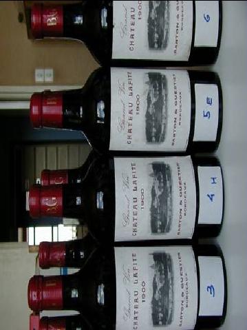
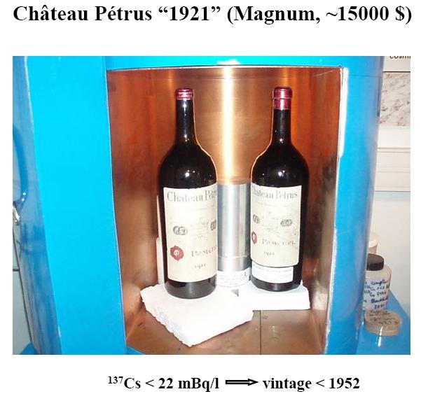
19 Applications Germanium detectors against wine swindles 137Cs 40K: 30Bq/l 137 Cs is man-made 29 authentic wines as reference If a wine is prenuclear-testing, there is no 137Cs. Comptes Rendus Physique, vol.10, no. 7, 622 (2009)
![Applications 137Cs Activity [mbq/l] 1Bq/l Nuclear Fallout If](/docs-images/95/123233379/images/20-3.jpg "somebody wants to sell you expensive vintage wine, have it")
20 Applications 137Cs Activity [mbq/l] 1Bq/l Nuclear Fallout If somebody wants to sell you expensive vintage wine, have it checked.


21 Applications Non destructive method! 137 Cs has 661 kev gamma line gammas make it easily through glass and wine 137Cs 40K

22 Applications
23 Applications

24 Applications Use the bottle itself got them
25 Applications The French like their salt radioactive!

26 Applications 226Ra mbq/kg French atlantic salts marine salts The true "fleur de sel" Portugese imposters 40K mbq/kg
27 Detector Systems Back to "normal" science: Nuclear Physics These things can built into large systems: But: Obviously there are some geometrical problems...


28 Gamma Tracking AGATA, the Advanced Gamma Tracking Array Cut crystals into shape needed and segment for tracking Form three groups of for packaging


29 Gamma Tracking AGATA, the Advanced Gamma Tracking Array 3 detectors in one cryostat 6 x 6 segments Very special detectors with extremely different segments and pulses. 90 mm 40mm
30 Germanium Detectors Let us come back to detectors: 3x3 cap true coax segmented homogenous electric field direct spatial information
31 p-type Detector Types n-type Passivation Lithium drift» 500 µm Boron implant» 500 nm p-type: holes centre n-type: holes mantle Segmentation mostly on n-type


32 Segmented Detectors p-type for a long time could not be segmented gracefully. Had to cut deep into the crystal... not good for field or durability! There is a way, but unproven.

33 Segmented Detectors n-type detectors are segmented in the implantation step: 3d segmented boron implantation is possible. [one reliable supplier only] Planar detectors are like silicon detectors [without industrial support].


34 Detector Types true coax cap coax point contact /BEGe weighting potential p p n + David Radford inverted coax does not have to be tempered n +
35 Pulse Shapes n-type The electrical field pulls the electrons to the core and the holes to the mantle. I use true coaxial detectors for illustrations. [simple field] Amplitude [arb. units] Core Amplitude [arb. units] Segment Get radial information from rise times Time [ns] Time [ns] 1~2 mm, but degenerate
36 Rise-time and Crystal Axis Amplitude [arb. units] Scan with Europium Source charge Time [ns] Avg. 10% - 90% risetime [ns] % f [DEG.]
37 Speed and Crystal Axis Speed Þ rise-time depends on angle between trajectory crystal axes Þ 110 electrons holes NIM A 569 (2006) 764
38 Trajectories Different speeds Þ bent trajectories Thesis: Jing Liu Electrons Holes
39 Pulse Shapes and Trajectories 40 Trajectory Holes Trajectory Electrons y [mm] segment boundary x [mm] Pulse Shapes are used to distinguish event classes. mirror charges


40 Final Remarks Germanium detectors are fascinating devices. They are wonderful tools to study radioactivity and trace gamma rays. Germanium detectors offer a lot of opportunity to further investigate Germanium properties: charge mobility, charge trapping, surface effects,.... They have many applications.
Semiconductor Detectors
 Semiconductor Detectors Summary of Last Lecture Band structure in Solids: Conduction band Conduction band thermal conductivity: E g > 5 ev Valence band Insulator Charge carrier in conductor: e - Charge
Chem 481 Lecture Material 3/20/09
 Chem 481 Lecture Material 3/20/09 Radiation Detection and Measurement Semiconductor Detectors The electrons in a sample of silicon are each bound to specific silicon atoms (occupy the valence band). If
Semiconductor Detectors
 Radiation Measurement Systems Semiconductor Detectors Ho Kyung Kim Pusan National University Semiconductors Differences btwn semiconductor & gas as a material for radiation detectors Higher (1,000 ) Free
Energetic particles and their detection in situ (particle detectors) Part II. George Gloeckler
 Part II. George Gloeckler") Energetic particles and their detection in situ (particle detectors) Part II George Gloeckler University of Michigan, Ann Arbor, MI University of Maryland, College Park, MD Simple particle detectors Gas-filled
Energetic particles and their detection in situ (particle detectors) Part II George Gloeckler University of Michigan, Ann Arbor, MI University of Maryland, College Park, MD Simple particle detectors Gas-filled
Advantages / Disadvantages of semiconductor detectors
 Advantages / Disadvantages of semiconductor detectors Semiconductor detectors have a high density (compared to gas detector) large energy loss in a short distance diffusion effect is smaller than in gas
Quality Assurance. Purity control. Polycrystalline Ingots
 Quality Assurance Purity control Polycrystalline Ingots 1 Gamma Spectrometry Nuclide Identification Detection of Impurity Traces 1.1 Nuclides Notation: Atomic Mass Atomic Number Element Neutron Atomic
Semiconductor X-Ray Detectors. Tobias Eggert Ketek GmbH
 Semiconductor X-Ray Detectors Tobias Eggert Ketek GmbH Semiconductor X-Ray Detectors Part A Principles of Semiconductor Detectors 1. Basic Principles 2. Typical Applications 3. Planar Technology 4. Read-out
Lecture 2. Introduction to semiconductors Structures and characteristics in semiconductors. Fabrication of semiconductor sensor
 Lecture 2 Introduction to semiconductors Structures and characteristics in semiconductors Semiconductor p-n junction Metal Oxide Silicon structure Semiconductor contact Fabrication of semiconductor sensor
DETECTORS. I. Charged Particle Detectors
 DETECTORS I. Charged Particle Detectors A. Scintillators B. Gas Detectors 1. Ionization Chambers 2. Proportional Counters 3. Avalanche detectors 4. Geiger-Muller counters 5. Spark detectors C. Solid State
Chap. 11 Semiconductor Diodes
 Chap. 11 Semiconductor Diodes Semiconductor diodes provide the best resolution for energy measurements, silicon based devices are generally used for charged-particles, germanium for photons. Scintillators
Lecture 18. New gas detectors Solid state trackers
 Lecture 18 New gas detectors Solid state trackers Time projection Chamber Full 3-D track reconstruction x-y from wires and segmented cathode of MWPC z from drift time de/dx information (extra) Drift over
Solid State Detectors
 Solid State Detectors Most material is taken from lectures by Michael Moll/CERN and Daniela Bortoletto/Purdue and the book Semiconductor Radiation Detectors by Gerhard Lutz. In gaseous detectors, a charged
Semiconductor-Detectors
 Semiconductor-Detectors 1 Motivation ~ 195: Discovery that pn-- junctions can be used to detect particles. Semiconductor detectors used for energy measurements ( Germanium) Since ~ 3 years: Semiconductor
ORTEC. Review of the Physics of Semiconductor Detectors. Interaction of Ionizing Radiation with Semiconductor Detectors. Heavy Charged Particles
 ORTEC Review of the Physics of Historically, semiconductor detectors were conceived as solid-state ionization chambers. To obtain a high-electric-field, low-current, solid-state device for detection and
Gamma and X-Ray Detection
 Gamma and X-Ray Detection DETECTOR OVERVIEW The kinds of detectors commonly used can be categorized as: a. Gas-filled Detectors b. Scintillation Detectors c. Semiconductor Detectors The choice of a particular
Positron Annihilation Spectroscopy
 Positron Annihilation Spectroscopy (1) Angular Correlation θ N x, y = p x, y m C θ γ-ray (511keV ± E) 0 (2) Doppler Broadening Cp E = z 2 θ N p ~100µm 22 Na (e + Source) e - e + ~ 10-12 s Sample γ-ray
Chapter 8 Hyper-Pure Germanium Detector
 Med Phys 4R06/6R03 Radioisotopes and Radiation Methodology 8-1 Chapter 8 Hyper-Pure Germanium Detector 8.1. Introduction Silicon semiconductor detectors described in the previous chapter have depletion
Chapter 8 Hyper-Pure Germanium Detector
 Med Phys 4RA3, 4RB3/6R03 Radioisotopes and Radiation Methodology 8-1 8.1. Introduction Chapter 8 Hyper-Pure Germanium Detector Silicon semiconductor detectors described in the previous chapter have depletion
Lecture 2. Introduction to semiconductors Structures and characteristics in semiconductors
 Lecture 2 Introduction to semiconductors Structures and characteristics in semiconductors Semiconductor p-n junction Metal Oxide Silicon structure Semiconductor contact Literature Glen F. Knoll, Radiation
Lecture 2. Introduction to semiconductors Structures and characteristics in semiconductors
 Lecture 2 Introduction to semiconductors Structures and characteristics in semiconductors Semiconductor p-n junction Metal Oxide Silicon structure Semiconductor contact Literature Glen F. Knoll, Radiation
Lecture 1. OUTLINE Basic Semiconductor Physics. Reading: Chapter 2.1. Semiconductors Intrinsic (undoped) silicon Doping Carrier concentrations
 silicon Doping Carrier concentrations") Lecture 1 OUTLINE Basic Semiconductor Physics Semiconductors Intrinsic (undoped) silicon Doping Carrier concentrations Reading: Chapter 2.1 EE105 Fall 2007 Lecture 1, Slide 1 What is a Semiconductor? Low
Lecture 1 OUTLINE Basic Semiconductor Physics Semiconductors Intrinsic (undoped) silicon Doping Carrier concentrations Reading: Chapter 2.1 EE105 Fall 2007 Lecture 1, Slide 1 What is a Semiconductor? Low
EECS130 Integrated Circuit Devices
 EECS130 Integrated Circuit Devices Professor Ali Javey 8/30/2007 Semiconductor Fundamentals Lecture 2 Read: Chapters 1 and 2 Last Lecture: Energy Band Diagram Conduction band E c E g Band gap E v Valence
Pulse-shape shape analysis with a Broad-energy. Ge-detector. Marik Schönert. MPI für f r Kernphysik Heidelberg
 Pulse-shape shape analysis with a Broad-energy Ge-detector Marik Barnabé é Heider Dušan Budjáš Oleg Chkvorets Stefan Schönert MPI für f r Kernphysik Heidelberg Outline 1. Motivation and goals 2. BEGe detector
n N D n p = n i p N A
 Summary of electron and hole concentration in semiconductors Intrinsic semiconductor: E G n kt i = pi = N e 2 0 Donor-doped semiconductor: n N D where N D is the concentration of donor impurity Acceptor-doped
Junction Diodes. Tim Sumner, Imperial College, Rm: 1009, x /18/2006
 Junction Diodes Most elementary solid state junction electronic devices. They conduct in one direction (almost correct). Useful when one converts from AC to DC (rectifier). But today diodes have a wide
Silicon Detectors in High Energy Physics
 Thomas Bergauer (HEPHY Vienna) IPM Teheran 22 May 2011 Sunday: Schedule Silicon Detectors in Semiconductor Basics (45 ) Detector concepts: Pixels and Strips (45 ) Coffee Break Strip Detector Performance
Electronics The basics of semiconductor physics
 Electronics The basics of semiconductor physics Prof. Márta Rencz, Gergely Nagy BME DED September 16, 2013 The basic properties of semiconductors Semiconductors conductance is between that of conductors
EECS143 Microfabrication Technology
 EECS143 Microfabrication Technology Professor Ali Javey Introduction to Materials Lecture 1 Evolution of Devices Yesterday s Transistor (1947) Today s Transistor (2006) Why Semiconductors? Conductors e.g
Introduction to Semiconductor Physics. Prof.P. Ravindran, Department of Physics, Central University of Tamil Nadu, India
 Introduction to Semiconductor Physics 1 Prof.P. Ravindran, Department of Physics, Central University of Tamil Nadu, India http://folk.uio.no/ravi/cmp2013 Review of Semiconductor Physics Semiconductor fundamentals
UNIVERSITY OF CALIFORNIA College of Engineering Department of Electrical Engineering and Computer Sciences. EECS 130 Professor Ali Javey Fall 2006
 UNIVERSITY OF CALIFORNIA College of Engineering Department of Electrical Engineering and Computer Sciences EECS 130 Professor Ali Javey Fall 2006 Midterm I Name: Closed book. One sheet of notes is allowed.
CLASS 12th. Semiconductors
 CLASS 12th Semiconductors 01. Distinction Between Metals, Insulators and Semi-Conductors Metals are good conductors of electricity, insulators do not conduct electricity, while the semiconductors have
EE143 Fall 2016 Microfabrication Technologies. Evolution of Devices
 EE143 Fall 2016 Microfabrication Technologies Prof. Ming C. Wu wu@eecs.berkeley.edu 511 Sutardja Dai Hall (SDH) 1-1 Evolution of Devices Yesterday s Transistor (1947) Today s Transistor (2006) 1-2 1 Why
First tests of the big volume ultra low background gamma spectrometer
 First tests of the big volume ultra low background gamma spectrometer N. Todorović,, D. MrđaM rđa,, I. Bikit, M. Vesković,, S. Forkapić,, J. Slivka Departman za fiziku, PMF, Novi Sad 1. Introduction Even
ECE 250 Electronic Devices 1. Electronic Device Modeling
 ECE 250 Electronic Devices 1 ECE 250 Electronic Device Modeling ECE 250 Electronic Devices 2 Introduction to Semiconductor Physics You should really take a semiconductor device physics course. We can only
3.1 Introduction to Semiconductors. Y. Baghzouz ECE Department UNLV
 3.1 Introduction to Semiconductors Y. Baghzouz ECE Department UNLV Introduction In this lecture, we will cover the basic aspects of semiconductor materials, and the physical mechanisms which are at the
Gamma-ray spectroscopy with the scintillator/photomultiplierand with the high purity Ge detector: Compton scattering, photoeffect, and pair production
 Experiment N2: Gamma-ray spectroscopy with the scintillator/photomultiplierand with the high purity Ge detector: Compton scattering, photoeffect, and pair production References: 1. Experiments in Nuclear
Radiation Detection for the Beta- Delayed Alpha and Gamma Decay of 20 Na. Ellen Simmons
 Radiation Detection for the Beta- Delayed Alpha and Gamma Decay of 20 Na Ellen Simmons 1 Contents Introduction Review of the Types of Radiation Charged Particle Radiation Detection Review of Semiconductor
HEROICA: a test facility for the characterization of BEGe detectors for the GERDA experiment
 Physikalisches Institut Kepler Center for Astro and Particle Physics : a test facility for the characterization of BEGe detectors for the GERDA experiment Raphael Falkenstein for the GERDA collaboration
Joint ICTP-IAEA Workshop on Physics of Radiation Effect and its Simulation for Non-Metallic Condensed Matter.
 2359-3 Joint ICTP-IAEA Workshop on Physics of Radiation Effect and its Simulation for Non-Metallic Condensed Matter 13-24 August 2012 Electrically active defects in semiconductors induced by radiation
Engineering 2000 Chapter 8 Semiconductors. ENG2000: R.I. Hornsey Semi: 1
 Engineering 2000 Chapter 8 Semiconductors ENG2000: R.I. Hornsey Semi: 1 Overview We need to know the electrical properties of Si To do this, we must also draw on some of the physical properties and we
PN Junction
 P Junction 2017-05-04 Definition Power Electronics = semiconductor switches are used Analogue amplifier = high power loss 250 200 u x 150 100 u Udc i 50 0 0 50 100 150 200 250 300 350 400 i,u dc i,u u
electronics fundamentals
 electronics fundamentals circuits, devices, and applications THOMAS L. FLOYD DAVID M. BUCHLA Lesson 1: Diodes and Applications Semiconductors Figure 1-1 The Bohr model of an atom showing electrons in orbits
Semiconductor Physics fall 2012 problems
 Semiconductor Physics fall 2012 problems 1. An n-type sample of silicon has a uniform density N D = 10 16 atoms cm -3 of arsenic, and a p-type silicon sample has N A = 10 15 atoms cm -3 of boron. For each
Digital Gamma-ray Spectroscopy & Imaging with Semiconductor detectors Frontiers of gamma-ray spectroscopy
 Digital Gamma-ray Spectroscopy & Imaging with Semiconductor detectors Frontiers of gamma-ray spectroscopy AGATA GRETA Dr Andy Boston ajboston@liv.ac.uk And its applications The AGATA Concept Without Compton
1 Name: Student number: DEPARTMENT OF PHYSICS AND PHYSICAL OCEANOGRAPHY MEMORIAL UNIVERSITY OF NEWFOUNDLAND. Fall :00-11:00
 1 Name: DEPARTMENT OF PHYSICS AND PHYSICAL OCEANOGRAPHY MEMORIAL UNIVERSITY OF NEWFOUNDLAND Final Exam Physics 3000 December 11, 2012 Fall 2012 9:00-11:00 INSTRUCTIONS: 1. Answer all seven (7) questions.
OPTI510R: Photonics. Khanh Kieu College of Optical Sciences, University of Arizona Meinel building R.626
 OPTI510R: Photonics Khanh Kieu College of Optical Sciences, University of Arizona kkieu@optics.arizona.edu Meinel building R.626 Announcements Homework #6 is assigned, due May 1 st Final exam May 8, 10:30-12:30pm
12/10/09. Chapter 18: Electrical Properties. View of an Integrated Circuit. Electrical Conduction ISSUES TO ADDRESS...
 Chapter 18: Electrical Properties ISSUES TO ADDRESS... How are electrical conductance and resistance characterized? What are the physical phenomena that distinguish? For metals, how is affected by and
Outline. Radiation Detectors. Radiation Detectors 1
 Outline Radiation Detectors Energy Resolution Detection Efficiency Dead Time Scintillation Detector Solid State Detectors Germanium Gamma Ray Detectors 2 Energy Resolution Energy Resolution For many applications
Radiation Detector 2016/17 (SPA6309)
") Radiation Detector 2016/17 (SPA6309) Semiconductor detectors (Leo, Chapter 10) 2017 Teppei Katori Semiconductor detectors are used in many situations, mostly for some kind of high precision measurement.
Radiation Detector 2016/17 (SPA6309) Semiconductor detectors (Leo, Chapter 10) 2017 Teppei Katori Semiconductor detectors are used in many situations, mostly for some kind of high precision measurement.
Study of PC-HPGe detector for dark matter search
 Study of PC-HPGe detector for dark matter search Yulan Li CDEX collaboration Research March 23-30, 2011, Beijing, China Outline What s a PC-HPGe detector? What we have done? Conclusion 2of 22 Point-contact
Electrical Resistance
 Electrical Resistance I + V _ W Material with resistivity ρ t L Resistance R V I = L ρ Wt (Unit: ohms) where ρ is the electrical resistivity 1 Adding parts/billion to parts/thousand of dopants to pure
Semiconductor Physics Problems 2015
 Semiconductor Physics Problems 2015 Page and figure numbers refer to Semiconductor Devices Physics and Technology, 3rd edition, by SM Sze and M-K Lee 1. The purest semiconductor crystals it is possible
Hussein Ayedh. PhD Studet Department of Physics
 Hussein Ayedh PhD Studet Department of Physics OUTLINE Introduction Semiconductors Basics DLTS Theory DLTS Requirements Example Summary Introduction Energetically "deep trapping levels in semiconductor
L03: pn Junctions, Diodes
 8/30/2012 Page 1 of 5 Reference:C:\Users\Bernhard Boser\Documents\Files\Lib\MathCAD\Default\defaults.mcd L03: pn Junctions, Diodes Intrinsic Si Q: What are n, p? Q: Is the Si charged? Q: How could we make
Solid State Physics SEMICONDUCTORS - IV. Lecture 25. A.H. Harker. Physics and Astronomy UCL
 Solid State Physics SEMICONDUCTORS - IV Lecture 25 A.H. Harker Physics and Astronomy UCL 9.9 Carrier diffusion and recombination Suppose we have a p-type semiconductor, i.e. n h >> n e. (1) Create a local
EE301 Electronics I , Fall
 EE301 Electronics I 2018-2019, Fall 1. Introduction to Microelectronics (1 Week/3 Hrs.) Introduction, Historical Background, Basic Consepts 2. Rewiev of Semiconductors (1 Week/3 Hrs.) Semiconductor materials
Semiconductor Devices and Circuits Fall Midterm Exam. Instructor: Dr. Dietmar Knipp, Professor of Electrical Engineering. Name: Mat. -Nr.
 Semiconductor Devices and Circuits Fall 2003 Midterm Exam Instructor: Dr. Dietmar Knipp, Professor of Electrical Engineering Name: Mat. -Nr.: Guidelines: Duration of the Midterm: 1 hour The exam is a closed
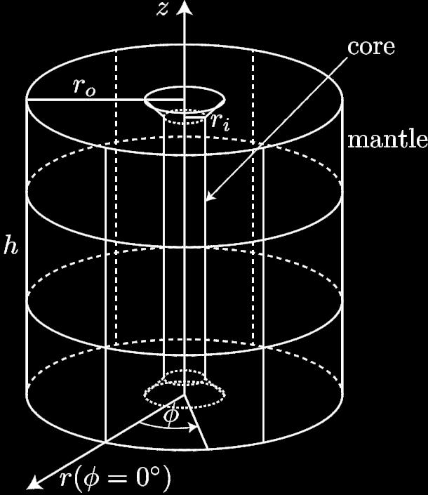
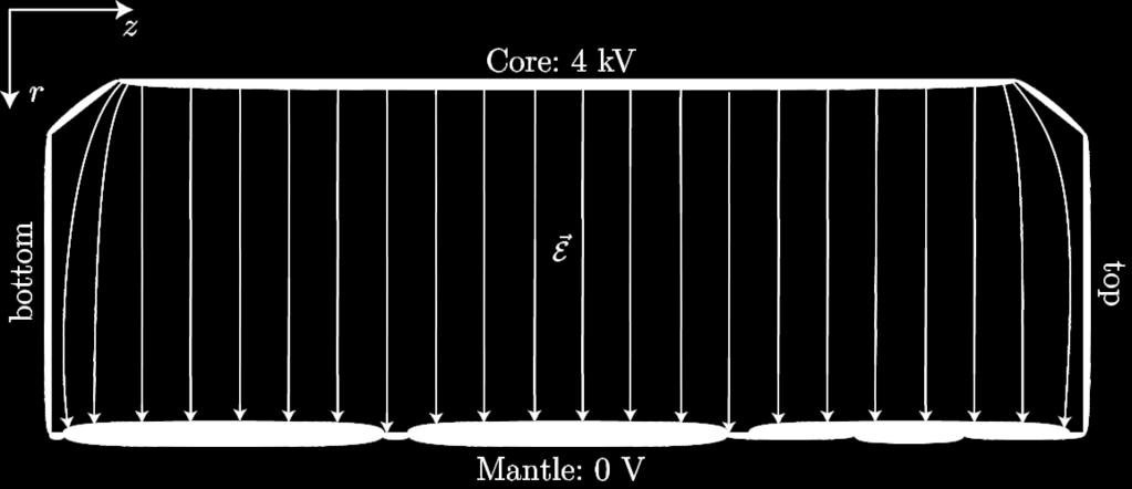
The GERDA Phase II detector assembly
 The GERDA Phase II detector assembly Tobias Bode 1, Carla Cattadori 2, Konstantin Gusev 1, Stefano Riboldi 2, Stefan Schönert 1, Bernhard Schwingenheuer 3 und Viktoria Wagner 3 for the GERDA collaboration
EEE4106Z Radiation Interactions & Detection
 EEE4106Z Radiation Interactions & Detection 2. Radiation Detection Dr. Steve Peterson 5.14 RW James Department of Physics University of Cape Town steve.peterson@uct.ac.za May 06, 2015 EEE4106Z :: Radiation
Semiconductor Physics. Lecture 3
 Semiconductor Physics Lecture 3 Intrinsic carrier density Intrinsic carrier density Law of mass action Valid also if we add an impurity which either donates extra electrons or holes the number of carriers
Misan University College of Engineering Electrical Engineering Department. Exam: Final semester Date: 17/6/2017
 Misan University College of Engineering Electrical Engineering Department Subject: Electronic I Class: 1 st stage Exam: Final semester Date: 17/6/2017 Examiner: Dr. Baqer. O. TH. Time: 3 hr. Note: Answer
Radioactivity. Lecture 6 Detectors and Instrumentation
 Radioactivity Lecture 6 Detectors and Instrumentation The human organs Neither humans nor animals have an organ for detecting radiation from radioactive decay! We can not hear it, smell it, feel it or
ESE 372 / Spring 2013 / Lecture 5 Metal Oxide Semiconductor Field Effect Transistor
 Metal Oxide Semiconductor Field Effect Transistor V G V G 1 Metal Oxide Semiconductor Field Effect Transistor We will need to understand how this current flows through Si What is electric current? 2 Back
Diffraction: spreading of waves around obstacles (EM waves, matter, or sound) Interference: the interaction of waves
 Interference: the interaction of waves") Diffraction & Interference Diffraction: spreading of waves around obstacles (EM waves, matter, or sound) Interference: the interaction of waves Diffraction in Nature What is Interference? The resultant
Diffraction & Interference Diffraction: spreading of waves around obstacles (EM waves, matter, or sound) Interference: the interaction of waves Diffraction in Nature What is Interference? The resultant
Semiconductor device structures are traditionally divided into homojunction devices
 0. Introduction: Semiconductor device structures are traditionally divided into homojunction devices (devices consisting of only one type of semiconductor material) and heterojunction devices (consisting
Session 6: Solid State Physics. Diode
 Session 6: Solid State Physics Diode 1 Outline A B C D E F G H I J 2 Definitions / Assumptions Homojunction: the junction is between two regions of the same material Heterojunction: the junction is between
Gamma-ray spectroscopy with the scintillator/photomultiplierand with the high purity Ge detector: Compton scattering, photoeffect, and pair production
 Experiment N2: Gamma-ray spectroscopy with the scintillator/photomultiplierand with the high purity Ge detector: Compton scattering, photoeffect, and pair production References: 1. Experiments in Nuclear
Semiconductor Device Physics
 1 Semiconductor Device Physics Lecture 3 http://zitompul.wordpress.com 2 0 1 3 Semiconductor Device Physics 2 Three primary types of carrier action occur inside a semiconductor: Drift: charged particle
EE 5344 Introduction to MEMS CHAPTER 5 Radiation Sensors
 EE 5344 Introduction to MEMS CHAPTER 5 Radiation Sensors 5. Radiation Microsensors Radiation µ-sensors convert incident radiant signals into standard electrical out put signals. Radiant Signals Classification
Electron Energy, E E = 0. Free electron. 3s Band 2p Band Overlapping energy bands. 3p 3s 2p 2s. 2s Band. Electrons. 1s ATOM SOLID.
 Electron Energy, E Free electron Vacuum level 3p 3s 2p 2s 2s Band 3s Band 2p Band Overlapping energy bands Electrons E = 0 1s ATOM 1s SOLID In a metal the various energy bands overlap to give a single
Components of a generic collider detector
 Lecture 24 Components of a generic collider detector electrons - ionization + bremsstrahlung photons - pair production in high Z material charged hadrons - ionization + shower of secondary interactions
Charge Carriers in Semiconductor
 Charge Carriers in Semiconductor To understand PN junction s IV characteristics, it is important to understand charge carriers behavior in solids, how to modify carrier densities, and different mechanisms
ITT Technical Institute ET215 Devices I Unit 1
 ITT Technical Institute ET215 Devices I Unit 1 Chapter 1 Chapter 2, Sections 2.1-2.4 Chapter 1 Basic Concepts of Analog Circuits Recall ET115 & ET145 Ohms Law I = V/R If voltage across a resistor increases
NUCL 3000/5030 Laboratory 2 Fall 2013
 Lab #2: Passive Gamma Spec Measurements in Decoding Natural Radioactivity in SLC Area Objectives a. Learn basics of gamma spectroscopy b. Learn the equipment in Counting stations #4, #5 and #8 c. Apply
Spring Semester 2012 Final Exam
 Spring Semester 2012 Final Exam Note: Show your work, underline results, and always show units. Official exam time: 2.0 hours; an extension of at least 1.0 hour will be granted to anyone. Materials parameters
Note that it is traditional to draw the diagram for semiconductors rotated 90 degrees, i.e. the version on the right above.
 5 Semiconductors The nearly free electron model applies equally in the case where the Fermi level lies within a small band gap (semiconductors), as it does when the Fermi level lies within a band (metal)
Lecture 2. Semiconductor Physics. Sunday 4/10/2015 Semiconductor Physics 1-1
 Lecture 2 Semiconductor Physics Sunday 4/10/2015 Semiconductor Physics 1-1 Outline Intrinsic bond model: electrons and holes Charge carrier generation and recombination Intrinsic semiconductor Doping:
Pulse Shape Analysis
 Pulse Shape Analysis Fabiana Cossavella Max-Planck Institut für Physik, München 26 March 2011 OUTLINE: motivation description of the procedure results Fabiana Cossavella Pulse Shape Analysis 1/11 Motivation:
Development of Radiation Hard Si Detectors
 Development of Radiation Hard Si Detectors Dr. Ajay K. Srivastava On behalf of Detector Laboratory of the Institute for Experimental Physics University of Hamburg, D-22761, Germany. Ajay K. Srivastava
ELECTRONIC I Lecture 1 Introduction to semiconductor. By Asst. Prof Dr. Jassim K. Hmood
 ELECTRONIC I Lecture 1 Introduction to semiconductor By Asst. Prof Dr. Jassim K. Hmood SOLID-STATE ELECTRONIC MATERIALS Electronic materials generally can be divided into three categories: insulators,
Physics 736. Experimental Methods in Nuclear-, Particle-, and Astrophysics
 Physics 736 Experimental Methods in Nuclear-, Particle-, and Astrophysics - Ionization & Semiconductor Detectors - Karsten Heeger heeger@wisc.edu Homework #6 Is due on Friday March 22 at 4.30pm Make-up
Doped Semiconductors *
 OpenStax-CNX module: m1002 1 Doped Semiconductors * Bill Wilson This work is produced by OpenStax-CNX and licensed under the Creative Commons Attribution License 1.0 To see how we can make silicon a useful
ECE 335: Electronic Engineering Lecture 2: Semiconductors
 Faculty of Engineering ECE 335: Electronic Engineering Lecture 2: Semiconductors Agenda Intrinsic Semiconductors Extrinsic Semiconductors N-type P-type Carrier Transport Drift Diffusion Semiconductors
The outline. 1) Detector parameters: efficiency, geometrical acceptance, dead-time, resolution, linearity. 2) gaseous ionization chambers
 Detector parameters: efficiency, geometrical acceptance, dead-time, resolution, linearity. 2) gaseous ionization chambers") The outline 1) Detector parameters: efficiency, geometrical acceptance, dead-time, resolution, linearity 2) gaseous ionization chambers 3) proportional counters- ionization measurement 4) silicon detectors
The outline 1) Detector parameters: efficiency, geometrical acceptance, dead-time, resolution, linearity 2) gaseous ionization chambers 3) proportional counters- ionization measurement 4) silicon detectors
Determination of properties in semiconductor materials by applying Matlab
 Determination of properties in semiconductor materials by applying Matlab Carlos Figueroa. 1, Raúl Riera A. 2 1 Departamento de Ingeniería Industrial. Universidad de Sonora A.P. 5-088, Hermosillo, Sonora.
High Purity Germanium Detector Calibration at ISOLDE
 High Purity Germanium Detector Calibration at ISOLDE Guðmundur Kári Stefánsson Summer Student of Maria Borge September 5, 2013 Abstract: This Summer Student Project involved the test and calibration of
Chapter 2 The Well 9/5/2017. E E 480 Introduction to Analog and Digital VLSI Paul M. Furth New Mexico State University
 hapter 2 The Well E E 480 Introduction to Analog and Digital VLSI Paul M. Furth New Mexico State University p+ sub ~ 150 m thick, p-epi ~ 30 m thick All transistors go in p- epi layer Typical p- doping
ISSUES TO ADDRESS...
 Chapter 12: Electrical Properties School of Mechanical Engineering Choi, Hae-Jin Materials Science - Prof. Choi, Hae-Jin Chapter 12-1 ISSUES TO ADDRESS... How are electrical conductance and resistance
Chapter 1 Overview of Semiconductor Materials and Physics
 Chapter 1 Overview of Semiconductor Materials and Physics Professor Paul K. Chu Conductivity / Resistivity of Insulators, Semiconductors, and Conductors Semiconductor Elements Period II III IV V VI 2 B
Session 5: Solid State Physics. Charge Mobility Drift Diffusion Recombination-Generation
 Session 5: Solid State Physics Charge Mobility Drift Diffusion Recombination-Generation 1 Outline A B C D E F G H I J 2 Mobile Charge Carriers in Semiconductors Three primary types of carrier action occur
A SEMICONDUCTOR DIODE. P-N Junction
 A SEMICONDUCTOR DIODE P-N Junction Analog Electronics Pujianto Department of Physics Edu. State University of Yogyakarta A Semiconductor Devices A Semiconductor devices can be defined as a unit which consists,
Semiconductors. Semiconductors also can collect and generate photons, so they are important in optoelectronic or photonic applications.
 Semiconductors Semiconducting materials have electrical properties that fall between true conductors, (like metals) which are always highly conducting and insulators (like glass or plastic or common ceramics)
arxiv:nucl-ex/ v1 4 Jan 2007
 Characterization of the first true coaxial 18-fold segmented n-type prototype detector for the GERDA project arxiv:nucl-ex/07004v1 4 Jan 2007 Abstract I. Abt a, A. Caldwell a, D. Gutknecht b, K. Kröninger
Lecture 8. Detectors for Ionizing Particles
 Lecture 8 Detectors for Ionizing Particles Content Introduction Overview of detector systems Sources of radiation Radioactive decay Cosmic Radiation Accelerators Interaction of Radiation with Matter General
Semiconductor Physics fall 2012 problems
 Semiconductor Physics fall 2012 problems 1. An n-type sample of silicon has a uniform density N D = 10 16 atoms cm -3 of arsenic, and a p-type silicon sample has N A = 10 15 atoms cm -3 of boron. For each
Semiconductor Detectors are Ionization Chambers. Detection volume with electric field Energy deposited positive and negative charge pairs
 1 V. Semiconductor Detectors V.1. Principles Semiconductor Detectors are Ionization Chambers Detection volume with electric field Energy deposited positive and negative charge pairs Charges move in field
Review of Semiconductor Drift Detectors
 Pavia October 25, 2004 Review of Semiconductor Drift Detectors Talk given by Pavel Rehak following a presentation on 5 th Hiroshima Symposium of Semiconductor Tracking Detectors Outline of the Review Principles
Quiz #1 Practice Problem Set
 Name: Student Number: ELEC 3908 Physical Electronics Quiz #1 Practice Problem Set? Minutes January 22, 2016 - No aids except a non-programmable calculator - All questions must be answered - All questions
Chapter 6: Basic radiation detectors
 Chapter 6: Basic radiation detectors Set of 60 slides based on the chapter authored by C.W.E. VAN EIJK Faculty of Applied Sciences, Delft University of Technology, Delft, Netherlands of the publication
A semiconductor is an almost insulating material, in which by contamination (doping) positive or negative charge carriers can be introduced.
 positive or negative charge carriers can be introduced.") Semiconductor A semiconductor is an almost insulating material, in which by contamination (doping) positive or negative charge carriers can be introduced. Page 2 Semiconductor materials Page 3 Energy levels
Semiconductor A semiconductor is an almost insulating material, in which by contamination (doping) positive or negative charge carriers can be introduced. Page 2 Semiconductor materials Page 3 Energy levels