Thermal Fluctuation-Induced Electricity Generation across a. Non-Ideal Diode
|
|
|
- Beverly Snow
- 6 years ago
- Views:
Transcription
1 Thermal Fluctuation-Induced Electricity Generation across a Non-Ideal Diode Guoan Tai, 1,2 Jinsong Liu, 1,3 Tian Zeng, 1,3 Jizhou Kong, 1,4 and Fuyong Lv 5 1 The State Key Laboratory of Mechanics and Control of Mechanical Structures, Nanjing University of Aeronautics and Astronautics, Nanjing , China 2 College of Aerospace Engineering, Nanjing University of Aeronautics and Astronautics, Nanjing , China 3 School of Material Science and Technology, Nanjing University of Aeronautics and Astronautics, Nanjing , China 4 College of Mechanical and Electrical Engineering, Nanjing University of Aeronautics and Astronautics, Nanjing , China 5 School of Electronic Science and Engineering, Southeast University, Nanjing , China We report experimentally that the electricity is generated from ambient thermal fluctuations across a non-ideal diode consisted of a silicon tip and an aluminum surface. The output is tuned by the contact force which modulates Schottky barrier heights as well as rectifying ratios of the diodes. The interaction regime between the silicon and the aluminum locates at the quantum-classical boundary where thermal fluctuations are appreciable, and the rectification of thermal fluctuations leads to the electricity generation. This finding offers an innovative approach to environmental energy harvesting. PACS numbers: Ln, Ca, Hp, a * To whom correspondence should be addressed. taiguoan@nuaa.edu.cn
2 As random deviations of a system from its average state, rectifying thermal fluctuations at the macroscale are believed to be impossible under thermal equilibrium conditions, nevertheless the case is completely different at a small scale [1-4]. As a system s spaces or dimensions decrease, the thermal fluctuations result in the system deviating from the thermodynamic equilibrium, and some useful and unexpected properties are usually predicted or observed in a nonequilibrium system [1,3]. For instance, extracting useful work from a single heat bath was predicted theoretically in quantum regime [5-7], and the erasure of quantum information has been ascribed experimentally to a source of entropy loss in the nonequilibrium system [8-10]. The decrease of entropy in the above systems were always explained by the rectification of microscopic thermal fluctuations as mentioned in many variants of the Maxwell s demon, such as thermal ratchets, Szilard's engine, quantum engine and the feedback control of microscopic fluctuations [5-16]. The nonequilibrium thermal fluctuations are appreciable at a small scale so that manipulating such small devices is very important for rectifying and harvesting the thermal fluctuations. Up to now, direct energy harvesting from thermal fluctuations in a small-scale device is not still reported experimentally in the absence of the external energy input. In this work, we report a process of harvesting energy from the ambient thermal fluctuations and transforming them into electricity by metal-semiconductor contacts. The output strikingly depends upon the contact force between the silicon tip and the aluminum surface. Weak asymmetry in the non-ideal diodes induces a nonequilibrium thermodynamic environment, leading to the electricity generation. This finding offers
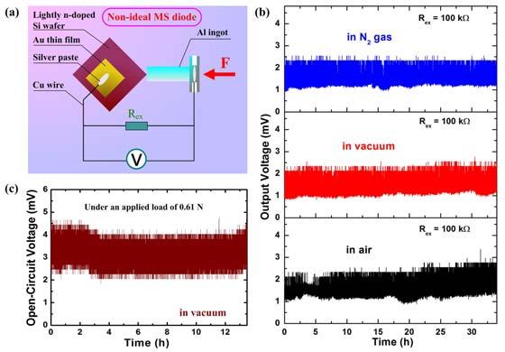
3 an innovative approach to environmental energy harvesting. Schematic diagram of the device and corresponding circuit were shown in Fig. 1(a), where the aluminum (Al) ingot was taken as the planar metal, and the lightly doped n-silicon (Si) (marked as n-si(4)) was used as the semiconductor tip [17]. The phase structure of the Al and the Si was examined by XRD analyses [17]. The output voltage (V op ) of the device with a 100 kω load and an applied force of 0.61 N fluctuated from 0.8 to 2.8 mv over 34 h under different atmospheric conditions including N 2 gas, vacuum and air in a black and sealed metal box (Fig. 1(b)), and the results show that the output is independent of the atmospheric conditions. The corresponding open-circuit voltage (V oc ) in vacuum fluctuated from 1.8 to 4.8 mv for over 10 h (Fig. 1(c)). The Al-Si contact degree was quantitatively characterized by the contact force. The V op values under N contact force was shown in Fig. 2(a), the higher V op ( mv) was observed at the contact force between 0.05 and 2.22 N, and the corresponding V oc displayed the same trend (Fig. 2(b)). The Al-Si contact characteristics were further evaluated by current-voltage (I-V) curves, as shown in Fig. 2(c). The asymmetry in the I-V curves is gradually removed with increasing contact force from 0.03 to 9.16 N, implying the decreasing of the Schottky barrier heights (SBHs), which is demonstrated by the calculated SBHs based on the thermionic emission theory [17]. The SBHs were closely correlated with the effective contact area (S eff ) [18,19], and the S eff was calculated by the Hertz theory [20] and then the penetration depth (D p ) was obtained, as shown in Fig. 2(d). In combination with Fig.
4 2(a), the output voltage was markedly higher than 0.53 mv when the D p is less than 1 µm which locates at the quantum-classical boundary, thus quantum decoherence is responsible for the electricity generation [5,6,21,22]. Subsequently, the SBHs and rectifying ratios were found to modulate from to ev and from 2.28 to 1.68, respectively (Fig. 2(e)) [17]. Compared with the rectifying ratio of an intimate standard diode (beyond 10 7 ) and an ideal Ohmic contact (10 0 ) [18], the experimental results suggest that we obtained the non-ideal diodes with tuning SBHs and rectifying ratios. The non-ideal diodes can be expressed by an equivalent circuit with the series and parallel resistances, and the resistances decrease with increasing the contact force (Fig. 2(f)) [17]. To ascertain why the continuous output was spontaneous in the non-ideal diodes, several experiments were performed. (1) The output of the Al-Si device was the same when the light was on and off [17]. (2) The output of a 100 kω resistor was close to zero, which excluded the possibility of the electricity generation from the thermal noise of the resistor [17]. (3) Temperature-dependent output data showed that the output was almost no difference under various temperatures, which results from a slight barrier height change with temperature [17-19]. Therefore, the spontaneously continuous output could be ascribed to an ambient thermal fluctuation in the non-ideal diodes. To reveal the underlying physical mechanism for the electricity generation, an ambient thermal fluctuation induced self-charging mechanism is therefore proposed to elucidate our experimental results. It is well-known that the free electrons with concentrations of up to /cm 3 on an intrinsic semiconductor Si surface are usually under thermal fluctuations with high speed (the most probable speed, v p = (2k B T
5 /m * ) 1/ m/s) at room temperature [18,19]. Probability distribution of the thermal fluctuations suggests that there are always some thermal electrons with high energy to go through the energy barrier, and the amount of the thermal electrons through the barrier strongly depends upon the barrier height [18,19]. For a non-ideal diode, previous theories implied that the temperature of the resistor is different from that of the diode, but the temperature difference is negligible because of far longer time scale of temperature relaxation (τ T ) than that of the heating time (τ H ) [23]. Experimentally, the energy harvesting process occurs spontaneously without external bias voltage and temperature difference, and the continuous output implies that the process involves a transition from classical equilibrium thermodynamics to nonequilibrium thermodynamics. For a classically intimate standard diode, the strict thermodynamic equilibrium state is well-established because of exactly balancing the electrostatic force by the diffusive force, where a depletion layer is invariably formed between a semiconductor and a metal or another semiconductor surfaces [18,19]. The layer blocks the flowing of the thermal electrons and builds up the barrier for modulating the electric transport by an applied electric field, and the barrier s energy difference is embodied as the SBH [18,19]. The depletion width (W D ), namely the width of the depletion region in a semiconductor, which is governed by the principle of charge neutrality, can be expressed as [18] W 2 kt ( V ) (1) Si 0 B D bi a qnd q where ε Si is the relative dielectric constant of the Si, ε 0 is the dielectric constant of vacuum, q is the elementary charge, N d is the impurity concentration, ψ bi is the built-in potential, V a is the applied electric field, k B is Boltzmann constant and T is the
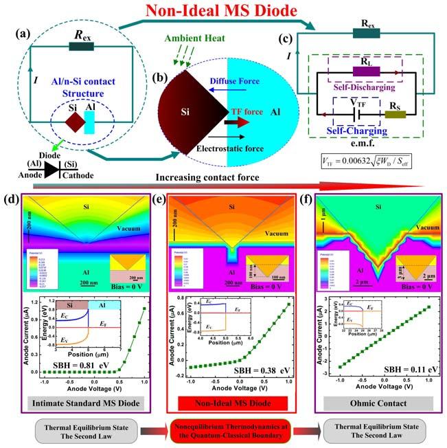
6 absolute temperature. The ψ bi is B0 ( kt B )ln( N c / N d ), where N c is the effective density of states in the conduction band of the n-si (N c = cm 3 ). When V a is zero, we calculated a series of W D based on Eq. (1) under different ψ bi values [17]. For the non-ideal Al-Si diode circuit (Fig. 3(a)), thermal fluctuation (TF) force in the system breaks the balance between the electrostatic force and the diffuse force, leading to the establishment of a nonequilibrium thermodynamic environment (Fig. 3(b)). Thus, the trend toward the thermodynamic equilibrium state and the persistently thermal fluctuation induce the energy harvesting. The corresponding equivalent circuit of the self-charging and self-discharging circle is proposed, where the self-charging process is maintained by the thermal fluctuations of electrons at the Si tip and the self-discharging behavior arises from the recovery toward the thermodynamic equilibrium state through the resistances (Fig. 3(c)), which is similar to that of our recent finding for the electricity generation from ionic thermal motion across a silicon surface [24]. To understand in detail the transition between the equilibrium and the nonequilibrium thermodynamics during the Al-Si contact, a two-dimensional Atlas electronic device numerical simulation was performed to obtain the potential distributions around the junctions, the I-V curves and the energy level diagrams. Three typical states were modeled: (i) a high SBH up to 0.81 ev when D p is zero (Fig. 3(d)); (ii) a moderate SBH equal to 0.38 ev when D p is 100 nm (Fig. 3(e)); (iii) a low SBH down to 0.11 ev when D p is 3 μm (Fig. 3(f)). Equipotential distributions near to the junctions are shown in Fig. 3(d-f) (top trace), and the dense equipotential lines,
7 especially at the edge of the contact, indicate a high electric field [17]. The I-V curve exhibits that state (i) is similar to a standard planar diode with a strong asymmetry, where the device is in a strict thermodynamic equilibrium (down trace, Fig. 3(d)) [17]. When the D p is less than one micrometer, the I-V curve of a non-ideal diode characteristic with the rectifying ratio down to 8 shows a weak asymmetry (down trace, Fig. 3(e)). Furthermore, after the D p is increased to three micrometers, the I-V curve with a symmetry suggests that the Ohmic contact is formed at the junction (Fig. 3(f)). The simulated results are in good agreement with our experiments. From the above, we know that the thermal fluctuations at the junction cannot be neglected for the nonequilibrium state located at the sub-micron interaction region. The junction situated in a thermal bath can be regarded as a small capacitor so that the thermal fluctuations of electrons inevitably change its voltage difference [25-28]. The averaged square of the thermal fluctuation voltage across the junction, 2 V TF, can be calculated as [26,28] V 4kTRf d (2) 2 B TF (2 fcr) (1 C / C0) where R is the resistance of the equivalent resistor, f and df are the frequency and the frequency interval of the resistor, respectively, and C and C 0 are the equivalent capacitance of the diode and the total capacitance of the diode, respectively. The C/C 0 term can be close to zero because C is far less than C 0, so we have V 2 TF k T C (3) B / The capacitance C is given by S S S C (4) eff eff eff Si 0 Si 0 Si 0 deff WTF WD
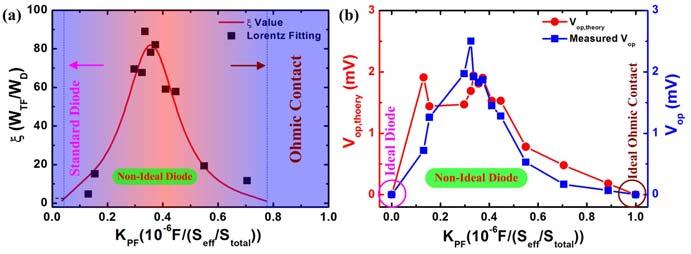
8 where S eff is the effective area of the junction, and d eff is the barrier width (equal to the depletion width of the junction in a standard Schottky diode), W TF is the width of a dynamical energy drop region in a nonequilibrium thermal fluctuation, W D is the depletion width in a strict thermodynamic equilibrium, and ξ is the thermal fluctuation factor (ξ = W TF /W D ). The ξ is unity for a strict thermodynamic equilibrium system, whereas it is usually larger than unity in a nonequilibrium thermodynamic one. The C reduces with decreasing S eff based on Eq. (4), and the small C makes the thermal voltage fluctuations appreciable when the junction is at the sub-micron scale [25-28]. The fluctuating thermal voltage (Unit: mv) was obtained by V TF ktw B TF Seff Si 0 1/ W / S D eff (5) Here, the V TF is equal to the measured V oc because the electricity generation arises from the thermal fluctuations. So, we calculated a series of the ξ versus the contact force according to Eq. (5) [17]. To investigate the feasible range of the ξ with respect to the high output, we define the pressure-related geometric factor K 10 F / ( S S ). The ξ is well-fitted as a function of K PF by a Lorentz 6 PF eff total function ξ = /(4(K PF ) ) (Fig. 4(a)), and the higher ξ dispersing around K PF =0.357 benefits the higher output, as the V op -K PF curve shown in Fig. 4(b). Based on Eq. (5) and the equivalent circuit in Fig. 3(c), the output voltage (V op,theory ) is given by R ex Vop,theory WD / Sef f Rin R ex (6) where R in is the internal resistance of the non-ideal diode, 1/ Rin 1/ RS 1/ RL. Comparing the measured V op,exp with the calculated V op,theory, we found that the proposed theory is in excellent agreement with the experimental results (Fig. 4(b))
9 [17]. The power density of the devices can be estimated by W V /( R S eff ), 2 oc in where W is the electrical power. The calculated maximum power density from our device is 32.3 μw/cm 2 under an applied force of 0.51 N. In addition, further studies showed that the output of the Al-Si devices strongly depended upon the doping concentration of the Si wafers [17]. Moreover, when the Al was substituted by other metals, the output was independent on their work functions, which is due to the pinning of the Fermi levels at the surfaces [17-19]. In conclusion, we have demonstrated the electricity generation from thermal fluctuation of electrons across a non-ideal metal-semiconductor diode under room temperature. The output is effectively tuned by the contact force which modulates the Schottky barrier heights as well as the rectifying ratios of the diodes. Quantum decoherence can be used to explain the electricity generation because the interaction regime locates at the quantum-classical boundary where thermal fluctuations are appreciable. The study builds a bridge between the classical equilibrium thermodynamics and the nonequilibrium thermodynamics, and offers an innovative approach to environmental energy harvesting. We thank Y. Xiao, T. Xu, Z. Xu and T. Sun and for many fruitful discussions. This work was supported by NSF ( ), Innovation Fund of NUAA (NS and NS ), the Research Funds of KL-INMD (NJ ), SKL-MCMS (0413Y02) and the Priority Academic Program Development of Jiangsu Higher Education Institutions.
10 [1] C. Jarzynski, Annu. Rev. Condens. Matter Phys. 2, 329 (2011). [2] C. Bustamante, J. Liphardt, and F. Ritort, Phys. Today 58, 43 (2005). [3] M. Esposito, U. Harbola, and S. Mukamel, Rev. Mod. Phys. 81, 1665 (2009). [4] G. M. Wang, E. M. Sevick, E. Mittag, D. J. Searles, and D. J. Evans, Phys. Rev. Lett. 89, (2002). [5] M. O. Scully, M. S. Zubairy, G. S. Agarwal, and H. Walther, Science 299, 862 (2003). [6] A. E. Allahverdyan and T. M. Nieuwenhuizen, Phys. Rev. Lett. 85, 1799 (2000). [7] M. O. Scully, Phys. Rev. Lett. 87, (2001). [8] V. Serreli, C. F. Lee, E. R. Kay, and D. A. Leigh, Nature 445, 523 (2007). [9] S. Toyabe, T. Sagawa, M. Ueda, E. Muneyuki, and M. Sano, Nat. Phys. 6, 988 (2010). [10] A. Bérut, A. Arakelyan, A. Petrosyan, S. Ciliberto, R. Dillenschneider, and E. Lutz, Nature 483, 187 (2012). [11] K. Maruyama, F. Nori, and V. Vedral, Rev. Mod. Phys. 81, 1 (2009). [12] P. Strasberg, G. Schaller, T. Brandes, and M. Esposito, Phys. Rev. Lett. 110, (2013). [13] D. Abreu and U. Seifert, Phys. Rev. Lett. 108, (2012). [14] T. Sagawa and M. Ueda, Phys. Rev. Lett. 109, (2012). [15] T. Sagawa and M. Ueda, Phys. Rev. Lett. 104, (2010). [16] T. Sagawa and M. Ueda, Phys. Rev. Lett. 100, (2008).
11 [17] See Supplemental Material at for technical details, discussion on the electricity generation mechanism, and the corresponding theoretical and experimental results. [18] S. M. Sze, Physics of Semiconductor Devices (John Wiley & Sons, New York, 2006). [19] D. K. Schroder, Semiconductor Material and Device Characterization (John Wiley & Sons, Inc., Hoboken, New Jersey, 2006). [20] B. Cappella and G. Dietler, Surf. Sci. Rep. 34, 1 (1999). [21] P. Bertet, S. Osnaghi, A. Rauschenbeutel, G. Nogues, A. Auffeves, M. Brune, J. M. Raimond, and S. Haroche, Nature 411, 166 (2001). [22] W. H. Zurek, Rev. Mod. Phys. 75, 715 (2003). [23] R. van Zon, S. Ciliberto, and E. G. D. Cohen, Phys. Rev. Lett. 92, (2004). [24] G. Tai, Z. H. Xu, and J. S. Liu, Appl. Phys. Lett. 103, (2013). [25] H. Xie and P. Sheng, Phys. Rev. B 79, (2009). [26] N. G. Van Kampen, Physica 26, 585 (1960). [27] P. Sheng, E. K. Sichel, and J. I. Gittleman, Phys. Rev. Lett. 40, 1191 (1978). [28] P. Sheng, Phys. Rev. B 21, 2180 (1980).
12 Figure legends FIG. 1 (color online). Experimental setup and output of the non-ideal Al-Si diode at room temperature. (a) Schematic diagram showing the experimental setup and the corresponding circuit. (b) Output voltage of the diode in N 2 gas, vacuum and air when a 100 kω resistor is in parallel loaded to the circuit. (c) Open-circuit voltage of the diode in vacuum. The applied force is 0.61 N. FIG. 2 (color online). Contact force-dependent output characteristics of the non-ideal Al-Si diodes. (a) The contact force-dependent output voltage of the diodes when a 100 kω resistor is loaded to the circuit. (b) The contact force-dependent open-circuit voltage of the diodes. (c) The contact force-dependent I-V characteristics of the diodes. The inset is an enlarge view of the curves with the voltage range from 0 to 0.4 V. (d) The contact force-dependent effective contact areas (S eff ) as well as penetration depths (D p ). (e) The contact force-dependent Schottky barrier heights (SBHs) as well as rectifying ratios. (f) The contact force-dependent series resistance (R s ) as well as parallel resistance (R L ). FIG. 3 (color online). Electricity generation mechanism of the non-ideal diodes. (a) A circuit diagram consisted of the Al-Si diode and the external load R ex. (b) The detail of the Al-Si junction, where the thermal fluctuation force is proposed to elucidate the electricity generation. (c) Equivalent circuit indicating the charging and discharging circle. (d) Top view: Calculated potential distribution of the ideal Al-Si Schottky contact. Bottom view: I-V characteristic of the device showing a high SBH of up to 0.81 ev and a high rectifying ratio on the order of 10 7 (strong asymmetry). (e) Top
13 view: Calculated potential distribution of the non-ideal Al-Si Schottky contact with the D p of 100 nm. Bottom view: I-V characteristic of the device showing a moderate SBH of 0.38 ev and a weak rectifying ratio of approx. 8 (weak asymmetry). (f) Top view: Calculated potential distribution of the ideal Al-Si Ohmic contact with the D p of 3 μm. Bottom view: I-V characteristic of the device showing a low SBH of 0.11 ev and a rectifying ratio of unity (strong symmetry). The insets in (d)-(f) are the corresponding energy band diagrams. FIG. 4 (color online). Pressure-related geometric factor dependence of thermal fluctuation parameters. (a) The thermal fluctuation factor (ξ) as a function of the pressure-related geometric factors (K PF ). The red line is a Lorentz fitting curve, and the horizontal dotted line is the thermodynamic equilibrium baseline. (b) Schottky barrier heights (SBHs) and rectifying ratios as functions of the pressure-related geometric factors. The SBHs and rectifying ratios of the ideal Schottky diode are set to be 0.81 ev and 10 7, respectively, whereas those of the ideal Ohmic contact are 0 ev and zero, respectively.
14 FIG.1
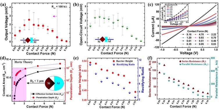
15 FIG. 2
16 FIG. 3
17 FIG. 4
Schottky Rectifiers Zheng Yang (ERF 3017,
 ECE442 Power Semiconductor Devices and Integrated Circuits Schottky Rectifiers Zheng Yang (ERF 3017, email: yangzhen@uic.edu) Power Schottky Rectifier Structure 2 Metal-Semiconductor Contact The work function
For the following statements, mark ( ) for true statement and (X) for wrong statement and correct it.
 for true statement and (X) for wrong statement and correct it.") Benha University Faculty of Engineering Shoubra Electrical Engineering Department First Year communications. Answer all the following questions Illustrate your answers with sketches when necessary. The
Benha University Faculty of Engineering Shoubra Electrical Engineering Department First Year communications. Answer all the following questions Illustrate your answers with sketches when necessary. The
Hardwiring Maxwell s Demon Tobias Brandes (Institut für Theoretische Physik, TU Berlin)
") Hardwiring Maxwell s Demon Tobias Brandes (Institut für Theoretische Physik, TU Berlin) Introduction. Feedback loops in transport by hand. by hardwiring : thermoelectric device. Maxwell demon limit. Co-workers:
Hardwiring Maxwell s Demon Tobias Brandes (Institut für Theoretische Physik, TU Berlin) Introduction. Feedback loops in transport by hand. by hardwiring : thermoelectric device. Maxwell demon limit. Co-workers:
arxiv: v2 [cond-mat.stat-mech] 9 Jul 2012
![arxiv: v2 [cond-mat.stat-mech] 9 Jul 2012](/thumbs/78/78428944.jpg "arxiv: v2 [cond-mat.stat-mech] 9 Jul 2012") epl draft Stochastic thermodynamics for Maxwell demon feedbacks arxiv:1204.5671v2 [cond-mat.stat-mech] 9 Jul 2012 Massimiliano sposito 1 and Gernot Schaller 2 1 Complex Systems and Statistical Mechanics,
epl draft Stochastic thermodynamics for Maxwell demon feedbacks arxiv:1204.5671v2 [cond-mat.stat-mech] 9 Jul 2012 Massimiliano sposito 1 and Gernot Schaller 2 1 Complex Systems and Statistical Mechanics,
Session 6: Solid State Physics. Diode
 Session 6: Solid State Physics Diode 1 Outline A B C D E F G H I J 2 Definitions / Assumptions Homojunction: the junction is between two regions of the same material Heterojunction: the junction is between
Metal Semiconductor Contacts
 Metal Semiconductor Contacts The investigation of rectification in metal-semiconductor contacts was first described by Braun [33-35], who discovered in 1874 the asymmetric nature of electrical conduction
Semiconductor Physics Problems 2015
 Semiconductor Physics Problems 2015 Page and figure numbers refer to Semiconductor Devices Physics and Technology, 3rd edition, by SM Sze and M-K Lee 1. The purest semiconductor crystals it is possible
Figure 3.1 (p. 141) Figure 3.2 (p. 142)
 Figure 3.2 (p. 142)") Figure 3.1 (p. 141) Allowed electronic-energy-state systems for two isolated materials. States marked with an X are filled; those unmarked are empty. System 1 is a qualitative representation of a metal;
Figure 3.1 (p. 141) Allowed electronic-energy-state systems for two isolated materials. States marked with an X are filled; those unmarked are empty. System 1 is a qualitative representation of a metal;
Sample Exam # 2 ECEN 3320 Fall 2013 Semiconductor Devices October 28, 2013 Due November 4, 2013
 Sample Exam # 2 ECEN 3320 Fall 203 Semiconductor Devices October 28, 203 Due November 4, 203. Below is the capacitance-voltage curve measured from a Schottky contact made on GaAs at T 300 K. Figure : Capacitance
Semiconductor Junctions
 8 Semiconductor Junctions Almost all solar cells contain junctions between different materials of different doping. Since these junctions are crucial to the operation of the solar cell, we will discuss
Maxwell's Demons and Quantum Heat Engines in Superconducting Circuits
 Maxwell's Demons and Quantum Heat Engines in Superconducting Circuits Jukka Pekola, Low Temperature Laboratory Aalto University, Helsinki, Finland Jonne Koski, now ETH Olli-Pentti Saira, now Caltech Ville
LECTURE 4: Information-powered refrigerators; quantum engines and refrigerators
 LECTURE 4: Information-powered refrigerators; quantum engines and refrigerators Fluctuation relations U. Seifert, Rep. Prog. Phys. 75, 126001 (2012) Fluctuation relations in a circuit Experiment on a double
Thermodynamic Computing. Forward Through Backwards Time by RocketBoom
 Thermodynamic Computing 1 14 Forward Through Backwards Time by RocketBoom The 2nd Law of Thermodynamics Clausius inequality (1865) S total 0 Total Entropy increases as time progresses Cycles of time R.Penrose
Semiconductor Physics fall 2012 problems
 Semiconductor Physics fall 2012 problems 1. An n-type sample of silicon has a uniform density N D = 10 16 atoms cm -3 of arsenic, and a p-type silicon sample has N A = 10 15 atoms cm -3 of boron. For each
Module-6: Schottky barrier capacitance-impurity concentration
 6.1 Introduction: Module-6: Schottky barrier capacitance-impurity concentration The electric current flowing across a metal semiconductor interface is generally non-linear with respect to the applied bias
Semiconductor Device Physics
 1 emiconductor Device Physics Lecture 8 http://zitompul.wordpress.com 2 0 1 3 emiconductor Device Physics 2 M Contacts and chottky Diodes 3 M Contact The metal-semiconductor (M) contact plays a very important
The physics of information: from Maxwell s demon to Landauer. Eric Lutz University of Erlangen-Nürnberg
 The physics of information: from Maxwell s demon to Landauer Eric Lutz University of Erlangen-Nürnberg Outline 1 Information and physics Information gain: Maxwell and Szilard Information erasure: Landauer
Semiconductor Detectors are Ionization Chambers. Detection volume with electric field Energy deposited positive and negative charge pairs
 1 V. Semiconductor Detectors V.1. Principles Semiconductor Detectors are Ionization Chambers Detection volume with electric field Energy deposited positive and negative charge pairs Charges move in field
A Bottom-gate Depletion-mode Nanowire Field Effect Transistor (NWFET) Model Including a Schottky Diode Model
 Model Including a Schottky Diode Model") Journal of the Korean Physical Society, Vol. 55, No. 3, September 2009, pp. 1162 1166 A Bottom-gate Depletion-mode Nanowire Field Effect Transistor (NWFET) Model Including a Schottky Diode Model Y. S.
Journal of the Korean Physical Society, Vol. 55, No. 3, September 2009, pp. 1162 1166 A Bottom-gate Depletion-mode Nanowire Field Effect Transistor (NWFET) Model Including a Schottky Diode Model Y. S.
UNIVERSITY OF CALIFORNIA, BERKELEY College of Engineering Department of Electrical Engineering and Computer Sciences
 UNIVERSITY OF CALIFORNIA, BERKELEY College of Engineering Department of Electrical Engineering and Computer Sciences EE 105: Microelectronic Devices and Circuits Spring 2008 MIDTERM EXAMINATION #1 Time
PHYSICAL ELECTRONICS(ECE3540) CHAPTER 9 METAL SEMICONDUCTOR AND SEMICONDUCTOR HETERO-JUNCTIONS
 CHAPTER 9 METAL SEMICONDUCTOR AND SEMICONDUCTOR HETERO-JUNCTIONS") PHYSICAL ELECTRONICS(ECE3540) CHAPTER 9 METAL SEMICONDUCTOR AND SEMICONDUCTOR HETERO-JUNCTIONS Tennessee Technological University Monday, November 11, 013 1 Introduction Chapter 4: we considered the semiconductor
PHYSICAL ELECTRONICS(ECE3540) CHAPTER 9 METAL SEMICONDUCTOR AND SEMICONDUCTOR HETERO-JUNCTIONS Tennessee Technological University Monday, November 11, 013 1 Introduction Chapter 4: we considered the semiconductor
Electronic transport in low dimensional systems
 Electronic transport in low dimensional systems For example: 2D system l
Junction Diodes. Tim Sumner, Imperial College, Rm: 1009, x /18/2006
 Junction Diodes Most elementary solid state junction electronic devices. They conduct in one direction (almost correct). Useful when one converts from AC to DC (rectifier). But today diodes have a wide
PHYSICAL ELECTRONICS(ECE3540) CHAPTER 9 METAL SEMICONDUCTOR AND SEMICONDUCTOR HETERO-JUNCTIONS
 CHAPTER 9 METAL SEMICONDUCTOR AND SEMICONDUCTOR HETERO-JUNCTIONS") PHYSICAL ELECTRONICS(ECE3540) CHAPTER 9 METAL SEMICONDUCTOR AND SEMICONDUCTOR HETERO-JUNCTIONS Tennessee Technological University Wednesday, October 30, 013 1 Introduction Chapter 4: we considered the
PHYSICAL ELECTRONICS(ECE3540) CHAPTER 9 METAL SEMICONDUCTOR AND SEMICONDUCTOR HETERO-JUNCTIONS Tennessee Technological University Wednesday, October 30, 013 1 Introduction Chapter 4: we considered the
Lecture 2. Introduction to semiconductors Structures and characteristics in semiconductors
 Lecture 2 Introduction to semiconductors Structures and characteristics in semiconductors Semiconductor p-n junction Metal Oxide Silicon structure Semiconductor contact Literature Glen F. Knoll, Radiation
OPTI510R: Photonics. Khanh Kieu College of Optical Sciences, University of Arizona Meinel building R.626
 OPTI510R: Photonics Khanh Kieu College of Optical Sciences, University of Arizona kkieu@optics.arizona.edu Meinel building R.626 Announcements Homework #6 is assigned, due May 1 st Final exam May 8, 10:30-12:30pm
Review Energy Bands Carrier Density & Mobility Carrier Transport Generation and Recombination
 Review Energy Bands Carrier Density & Mobility Carrier Transport Generation and Recombination The Metal-Semiconductor Junction: Review Energy band diagram of the metal and the semiconductor before (a)
1 Name: Student number: DEPARTMENT OF PHYSICS AND PHYSICAL OCEANOGRAPHY MEMORIAL UNIVERSITY OF NEWFOUNDLAND. Fall :00-11:00
 1 Name: DEPARTMENT OF PHYSICS AND PHYSICAL OCEANOGRAPHY MEMORIAL UNIVERSITY OF NEWFOUNDLAND Final Exam Physics 3000 December 11, 2012 Fall 2012 9:00-11:00 INSTRUCTIONS: 1. Answer all seven (7) questions.
Characteristics and parameter extraction for NiGe/n-type Ge Schottky diode with variable annealing temperatures
 034 Chin. Phys. B Vol. 19, No. 5 2010) 057303 Characteristics and parameter extraction for NiGe/n-type Ge Schottky diode with variable annealing temperatures Liu Hong-Xia ), Wu Xiao-Feng ), Hu Shi-Gang
Semiconductor Detectors
 Semiconductor Detectors Summary of Last Lecture Band structure in Solids: Conduction band Conduction band thermal conductivity: E g > 5 ev Valence band Insulator Charge carrier in conductor: e - Charge
High-temperature characteristics of SiC Schottky barrier diodes related to physical phenomena
 High-temperature characteristics of SiC Schottky barrier diodes related to physical phenomena Tsuyoshi Funaki 1a), Tsunenobu Kimoto 2, and Takashi Hikihara 1 1 Kyoto University, Dept. of Electrical Eng.
ECE-342 Test 2 Solutions, Nov 4, :00-8:00pm, Closed Book (one page of notes allowed)
") ECE-342 Test 2 Solutions, Nov 4, 2008 6:00-8:00pm, Closed Book (one page of notes allowed) Please use the following physical constants in your calculations: Boltzmann s Constant: Electron Charge: Free
ECE-342 Test 2 Solutions, Nov 4, 2008 6:00-8:00pm, Closed Book (one page of notes allowed) Please use the following physical constants in your calculations: Boltzmann s Constant: Electron Charge: Free
Effective masses in semiconductors
 Effective masses in semiconductors The effective mass is defined as: In a solid, the electron (hole) effective mass represents how electrons move in an applied field. The effective mass reflects the inverse
n N D n p = n i p N A
 Summary of electron and hole concentration in semiconductors Intrinsic semiconductor: E G n kt i = pi = N e 2 0 Donor-doped semiconductor: n N D where N D is the concentration of donor impurity Acceptor-doped
Semiconductor Physics fall 2012 problems
 Semiconductor Physics fall 2012 problems 1. An n-type sample of silicon has a uniform density N D = 10 16 atoms cm -3 of arsenic, and a p-type silicon sample has N A = 10 15 atoms cm -3 of boron. For each
ECE 340 Lecture 35 : Metal- Semiconductor Junctions Class Outline:
 ECE 340 Lecture 35 : - Junctions Class Outline: Ideal - Contacts Rectifying Contacts Ohmic Contacts Things you should know when you leave Key Questions What happens to the bands when we make contact between
EE 130 Intro to MS Junctions Week 6 Notes. What is the work function? Energy to excite electron from Fermi level to the vacuum level
 EE 13 Intro to S Junctions eek 6 Notes Problem 1 hat is the work function? Energy to ecite electron from Fermi level to the vacuum level Electron affinity of 4.5eV Electron affinity of Ge 4.eV orkfunction
UNIVERSITY OF CALIFORNIA College of Engineering Department of Electrical Engineering and Computer Sciences. EECS 130 Professor Ali Javey Fall 2006
 UNIVERSITY OF CALIFORNIA College of Engineering Department of Electrical Engineering and Computer Sciences EECS 130 Professor Ali Javey Fall 2006 Midterm 2 Name: SID: Closed book. Two sheets of notes are
(a) (b) Supplementary Figure 1. (a) (b) (a) Supplementary Figure 2. (a) (b) (c) (d) (e)
 (b) Supplementary Figure 1. (a) (b) (a) Supplementary Figure 2. (a) (b) (c) (d) (e)") (a) (b) Supplementary Figure 1. (a) An AFM image of the device after the formation of the contact electrodes and the top gate dielectric Al 2 O 3. (b) A line scan performed along the white dashed line
(a) (b) Supplementary Figure 1. (a) An AFM image of the device after the formation of the contact electrodes and the top gate dielectric Al 2 O 3. (b) A line scan performed along the white dashed line
ECE PN Junctions and Diodes
 ECE 342 2. PN Junctions and iodes Jose E. Schutt-Aine Electrical & Computer Engineering University of Illinois jschutt@emlab.uiuc.edu ECE 342 Jose Schutt Aine 1 B: material dependent parameter = 5.4 10
Self-Charged Graphene Battery Harvests Electricity. from Thermal Energy of the Environment
 Self-Charged Graphene Battery Harvests Electricity from Thermal Energy of the Environment Zihan Xu 1 *, Guoan Tai 1,3, Yungang Zhou 2, Fei Gao 2, Kim Hung Wong 1 1 Department of Applied Physics and Materials
Closed-loop analysis of a thermo-charged capacitor
 Closed-loop analysis of a thermo-charged capacitor arxiv:1407.6627v2 [physics.gen-ph] 4 May 2015 Germano D Abramo Istituto Nazionale di Astrofisica, Roma, Italy E mail: Germano.Dabramo@iaps.inaf.it Abstract
Midterm I - Solutions
 UNIVERSITY OF CALIFORNIA College of Engineering Department of Electrical Engineering and Computer Sciences EECS 130 Spring 2008 Professor Chenming Hu Midterm I - Solutions Name: SID: Grad/Undergrad: Closed
Spring Semester 2012 Final Exam
 Spring Semester 2012 Final Exam Note: Show your work, underline results, and always show units. Official exam time: 2.0 hours; an extension of at least 1.0 hour will be granted to anyone. Materials parameters
Lecture 2. Introduction to semiconductors Structures and characteristics in semiconductors
 Lecture 2 Introduction to semiconductors Structures and characteristics in semiconductors Semiconductor p-n junction Metal Oxide Silicon structure Semiconductor contact Literature Glen F. Knoll, Radiation
Schottky Diodes (M-S Contacts)
") Schottky Diodes (M-S Contacts) Three MITs of the Day Band diagrams for ohmic and rectifying Schottky contacts Similarity to and difference from bipolar junctions on electrostatic and IV characteristics.
Schottky Diodes (M-S Contacts) Three MITs of the Day Band diagrams for ohmic and rectifying Schottky contacts Similarity to and difference from bipolar junctions on electrostatic and IV characteristics.
System Modeling and Characterization of SiC Schottky Power Diodes
 System Modeling and Characterization of SiC Schottky Power Diodes Hui Zhang, Student Member, IEEE, Leon M. Tolbert, Senior Member, IEEE, Burak Ozpineci, Senior Member, IEEE Abstract-Most of the present
arxiv: v1 [cond-mat.stat-mech] 8 Jul 2013
![arxiv: v1 [cond-mat.stat-mech] 8 Jul 2013](/thumbs/88/116051609.jpg "arxiv: v1 [cond-mat.stat-mech] 8 Jul 2013") Maxwell s Refrigerator: An Exactly Solvable Model Dibyendu Mandal 1, H. T. Quan,3 and Christopher Jarzynski,4 1 Department of Physics, University of Maryland, College Park, Maryland 074, U.S.A. Department
Maxwell s Refrigerator: An Exactly Solvable Model Dibyendu Mandal 1, H. T. Quan,3 and Christopher Jarzynski,4 1 Department of Physics, University of Maryland, College Park, Maryland 074, U.S.A. Department
L03: pn Junctions, Diodes
 8/30/2012 Page 1 of 5 Reference:C:\Users\Bernhard Boser\Documents\Files\Lib\MathCAD\Default\defaults.mcd L03: pn Junctions, Diodes Intrinsic Si Q: What are n, p? Q: Is the Si charged? Q: How could we make
Maxwell's Demon in Biochemical Signal Transduction
 Maxwell's Demon in Biochemical Signal Transduction Takahiro Sagawa Department of Applied Physics, University of Tokyo New Frontiers in Non-equilibrium Physics 2015 28 July 2015, YITP, Kyoto Collaborators
Lecture 2. Introduction to semiconductors Structures and characteristics in semiconductors. Fabrication of semiconductor sensor
 Lecture 2 Introduction to semiconductors Structures and characteristics in semiconductors Semiconductor p-n junction Metal Oxide Silicon structure Semiconductor contact Fabrication of semiconductor sensor
Nonequilibrium Thermodynamics of Small Systems: Classical and Quantum Aspects. Massimiliano Esposito
 Nonequilibrium Thermodynamics of Small Systems: Classical and Quantum Aspects Massimiliano Esposito Paris May 9-11, 2017 Introduction Thermodynamics in the 19th century: Thermodynamics in the 21th century:
Al/Ti/4H SiC Schottky barrier diodes with inhomogeneous barrier heights
 Al/Ti/4H SiC Schottky barrier diodes with inhomogeneous barrier heights Wang Yue-Hu( ), Zhang Yi-Men( ), Zhang Yu-Ming( ), Song Qing-Wen( ), and Jia Ren-Xu( ) School of Microelectronics and Key Laboratory
UNIVERSITY OF CALIFORNIA College of Engineering Department of Electrical Engineering and Computer Sciences. EECS 130 Professor Ali Javey Fall 2006
 UNIVERSITY OF CALIFORNIA College of Engineering Department of Electrical Engineering and Computer Sciences EECS 130 Professor Ali Javey Fall 2006 Midterm I Name: Closed book. One sheet of notes is allowed.
Schottky diodes. JFETs - MESFETs - MODFETs
 Technische Universität Graz Institute of Solid State Physics Schottky diodes JFETs - MESFETs - MODFETs Quasi Fermi level When the charge carriers are not in equilibrium the Fermi energy can be different
Modified Mott-Schottky Analysis of Nanocrystal Solar Cells
 Modified Mott-Schottky Analysis of Nanocrystal Solar Cells S. M. Willis, C. Cheng, H. E. Assender and A. A. R. Watt Department of Materials, University of Oxford, Parks Road, Oxford. OX1 3PH. United Kingdom
Preliminary measurements of charge collection and DLTS analysis of p + /n junction SiC detectors and simulations of Schottky diodes
 Preliminary measurements of charge collection and DLTS analysis of p + /n junction SiC detectors and simulations of Schottky diodes F.Moscatelli, A.Scorzoni, A.Poggi, R.Nipoti DIEI and INFN Perugia and
Fermi Level Pinning at Electrical Metal Contacts. of Monolayer Molybdenum Dichalcogenides
 Supporting information Fermi Level Pinning at Electrical Metal Contacts of Monolayer Molybdenum Dichalcogenides Changsik Kim 1,, Inyong Moon 1,, Daeyeong Lee 1, Min Sup Choi 1, Faisal Ahmed 1,2, Seunggeol
Final Examination EE 130 December 16, 1997 Time allotted: 180 minutes
 Final Examination EE 130 December 16, 1997 Time allotted: 180 minutes Problem 1: Semiconductor Fundamentals [30 points] A uniformly doped silicon sample of length 100µm and cross-sectional area 100µm 2
Graphene photodetectors with ultra-broadband and high responsivity at room temperature
 SUPPLEMENTARY INFORMATION DOI: 10.1038/NNANO.2014.31 Graphene photodetectors with ultra-broadband and high responsivity at room temperature Chang-Hua Liu 1, You-Chia Chang 2, Ted Norris 1.2* and Zhaohui
Section 12: Intro to Devices
 Section 12: Intro to Devices Extensive reading materials on reserve, including Robert F. Pierret, Semiconductor Device Fundamentals Bond Model of Electrons and Holes Si Si Si Si Si Si Si Si Si Silicon
A study of the silicon Bulk-Barrier Diodes designed in planar technology by means of simulation
 Journal of Engineering Science and Technology Review 2 (1) (2009) 157-164 Research Article JOURNAL OF Engineering Science and Technology Review www.jestr.org A study of the silicon Bulk-Barrier Diodes
CMOS Devices. PN junctions and diodes NMOS and PMOS transistors Resistors Capacitors Inductors Bipolar transistors
 CMOS Devices PN junctions and diodes NMOS and PMOS transistors Resistors Capacitors Inductors Bipolar transistors PN Junctions Diffusion causes depletion region D.R. is insulator and establishes barrier
The pn junction. [Fonstad, Ghione]
![The pn junction. [Fonstad, Ghione]](/thumbs/93/112370833.jpg "The pn junction. [Fonstad, Ghione]") The pn junction [Fonstad, Ghione] Band diagram On the vertical axis: potential energy of the electrons On the horizontal axis: now there is nothing: later we ll put the position qf s : work function (F
The pn junction [Fonstad, Ghione] Band diagram On the vertical axis: potential energy of the electrons On the horizontal axis: now there is nothing: later we ll put the position qf s : work function (F
8. Schottky contacts / JFETs
 Technische Universität Graz Institute of Solid State Physics 8. Schottky contacts / JFETs Nov. 21, 2018 Technische Universität Graz Institute of Solid State Physics metal - semiconductor contacts Photoelectric
Song and Feng Pan b) * Laboratory of Advanced Materials (MOE), School of Materials Science and Engineering,
 * Laboratory of Advanced Materials (MOE), School of Materials Science and Engineering,") Electronic Supplementary Material (ESI) for Nanoscale. This journal is The Royal Society of Chemistry 2015 Supplementary Information to Forming-free and self-rectifying resistive switching of the simple
Electronic Supplementary Material (ESI) for Nanoscale. This journal is The Royal Society of Chemistry 2015 Supplementary Information to Forming-free and self-rectifying resistive switching of the simple
junctions produce nonlinear current voltage characteristics which can be exploited
 Chapter 6 P-N DODES Junctions between n-and p-type semiconductors are extremely important foravariety of devices. Diodes based on p-n junctions produce nonlinear current voltage characteristics which can
Current mechanisms Exam January 27, 2012
 Current mechanisms Exam January 27, 2012 There are four mechanisms that typically cause currents to flow: thermionic emission, diffusion, drift, and tunneling. Explain briefly which kind of current mechanisms
Edge termination study and fabrication of a 4H SiC junction barrier Schottky diode
 Edge termination study and fabrication of a 4H SiC junction barrier Schottky diode Chen Feng-Ping( ) a), Zhang Yu-Ming( ) a), Zhang Yi-Men( ) a), Tang Xiao-Yan( ) a), Wang Yue-Hu( ) a), and Chen Wen-Hao(
Electronic Supporting Information
 Characterization of Planar Lead Halide Perovskite Solar Cells by Impedance Spectroscopy, Open Circuit Photovoltage Decay and Intensity-Modulated Photovoltage/Photocurrent Spectroscopy Adam Pockett 1, Giles
Semiconductor device structures are traditionally divided into homojunction devices
 0. Introduction: Semiconductor device structures are traditionally divided into homojunction devices (devices consisting of only one type of semiconductor material) and heterojunction devices (consisting
Electronic Circuits for Mechatronics ELCT 609 Lecture 2: PN Junctions (1)
") Electronic Circuits for Mechatronics ELCT 609 Lecture 2: PN Junctions (1) Assistant Professor Office: C3.315 E-mail: eman.azab@guc.edu.eg 1 Electronic (Semiconductor) Devices P-N Junctions (Diodes): Physical
Electronic Circuits for Mechatronics ELCT 609 Lecture 2: PN Junctions (1) Assistant Professor Office: C3.315 E-mail: eman.azab@guc.edu.eg 1 Electronic (Semiconductor) Devices P-N Junctions (Diodes): Physical
Fabrication of a 600V/20A 4H-SiC Schottky Barrier Diode
 Fabrication of a 600V/20A 4H-SiC Schottky Barrier Diode In-Ho Kang, Sang-Cheol Kim, Jung-Hyeon Moon, Wook Bahng, and Nam-Kyun Kim Power Ssemiconductor Research Center, Korea Electrotechnology Research
Electronic Supplementary Information. Recombination kinetics in silicon solar cell under low-concentration: Electroanalytical
 Electronic Supplementary Material (ESI) for Physical Chemistry Chemical Physics. This journal is the Owner Societies 2014 Electronic Supplementary Information Recombination kinetics in silicon solar cell
III.6. METAL SEMICONDUCTOR CONTACT BIAS
 .6. MEAL SEMCONUCOR CONAC BAS 1. Work purpose he determination of the potential difference that appears at the contact surface between a metal and a semiconductor, potential difference that is known under
6.012 Electronic Devices and Circuits
 Page 1 of 1 YOUR NAME Department of Electrical Engineering and Computer Science Massachusetts Institute of Technology 6.12 Electronic Devices and Circuits Exam No. 1 Wednesday, October 7, 29 7:3 to 9:3
EECS130 Integrated Circuit Devices
 EECS130 Integrated Circuit Devices Professor Ali Javey 10/02/2007 MS Junctions, Lecture 2 MOS Cap, Lecture 1 Reading: finish chapter14, start chapter16 Announcements Professor Javey will hold his OH at
8.1 Drift diffusion model
 8.1 Drift diffusion model Advanced theory 1 Basic Semiconductor Equations The fundamentals of semiconductor physic are well described by tools of quantum mechanic. This point of view gives us a model of
Lecture 9: Metal-semiconductor junctions
 Lecture 9: Metal-semiconductor junctions Contents 1 Introduction 1 2 Metal-metal junction 1 2.1 Thermocouples.......................... 2 3 Schottky junctions 4 3.1 Forward bias............................
SUPPLEMENTARY FIGURES
 1 SUPPLEMENTARY FIGURES Supplementary Figure 1: Schematic representation of the experimental set up. The PC of the hot line being biased, the temperature raises. The temperature is extracted from noise
Thermal Noise Driven Heat Engines
 The important thing is not to stop questioning. uriosity has its own reason for existing. (Albert Einstein) Thermal Noise Driven Heat Engines L.B. Kish Department of Electrical and omputer Engineering,
Electrostatics of Nanowire Transistors
 Electrostatics of Nanowire Transistors Jing Guo, Jing Wang, Eric Polizzi, Supriyo Datta and Mark Lundstrom School of Electrical and Computer Engineering Purdue University, West Lafayette, IN, 47907 ABSTRACTS
Diodes for Power Electronic Applications
 Lecture Notes Diodes for Power Electronic Applications William P. Robbins Professor, Dept. of Electrical and Computer Engineering University of Minnesota OUTLINE PN junction power diode construction Breakdown
Information Thermodynamics on Causal Networks
 1/39 Information Thermodynamics on Causal Networks FSPIP 2013, July 12 2013. Sosuke Ito Dept. of Phys., the Univ. of Tokyo (In collaboration with T. Sagawa) ariv:1306.2756 The second law of thermodynamics
Solid State Electronics. Final Examination
 The University of Toledo EECS:4400/5400/7400 Solid State Electronic Section elssf08fs.fm - 1 Solid State Electronics Final Examination Problems Points 1. 1. 14 3. 14 Total 40 Was the exam fair? yes no
Hussein Ayedh. PhD Studet Department of Physics
 Hussein Ayedh PhD Studet Department of Physics OUTLINE Introduction Semiconductors Basics DLTS Theory DLTS Requirements Example Summary Introduction Energetically "deep trapping levels in semiconductor
EE 5611 Introduction to Microelectronic Technologies Fall Tuesday, September 23, 2014 Lecture 07
 EE 5611 Introduction to Microelectronic Technologies Fall 2014 Tuesday, September 23, 2014 Lecture 07 1 Introduction to Solar Cells Topics to be covered: Solar cells and sun light Review on semiconductor
UNIVERSITY OF CALIFORNIA, BERKELEY College of Engineering Department of Electrical Engineering and Computer Sciences
 UNIVERSITY OF CALIFORNIA, BERKELEY College of Engineering Department of Electrical Engineering and Computer Sciences EECS 40 Spring 2000 Introduction to Microelectronic Devices Prof. King MIDTERM EXAMINATION
Lecture 19 - p-n Junction (cont.) October 18, Ideal p-n junction out of equilibrium (cont.) 2. pn junction diode: parasitics, dynamics
 October 18, Ideal p-n junction out of equilibrium (cont.) 2. pn junction diode: parasitics, dynamics") 6.720J/3.43J - Integrated Microelectronic Devices - Fall 2002 Lecture 19-1 Lecture 19 - p-n Junction (cont.) October 18, 2002 Contents: 1. Ideal p-n junction out of equilibrium (cont.) 2. pn junction diode:
6.720J/3.43J - Integrated Microelectronic Devices - Fall 2002 Lecture 19-1 Lecture 19 - p-n Junction (cont.) October 18, 2002 Contents: 1. Ideal p-n junction out of equilibrium (cont.) 2. pn junction diode:
DEMONS: MAXWELL S DEMON, SZILARD S ENGINE AND LANDAUER S ERASURE DISSIPATION
 In: Proceedings of the first conference on Hot Topics in Physical Informatics (HoTPI, 2013 November). Paper is in press at International Journal of Modern Physics: Conference Series (2014). DEMONS: MAXWELL
Quantitative Scanning Capacitance Spectroscopy on GaAs and InAs Quantum Dots
 Quantitative Scanning Capacitance Spectroscopy on GaAs and InAs Quantum Dots W. Brezna, T. Roch, G. Strasser, J. Smoliner Institute of Solid State Electronics Vienna University of Technology, A-1040 Vienna,
single-electron electron tunneling (SET)
") single-electron electron tunneling (SET) classical dots (SET islands): level spacing is NOT important; only the charging energy (=classical effect, many electrons on the island) quantum dots: : level spacing
single-electron electron tunneling (SET) classical dots (SET islands): level spacing is NOT important; only the charging energy (=classical effect, many electrons on the island) quantum dots: : level spacing
Ch/ChE 140a Problem Set #3 2007/2008 SHOW ALL OF YOUR WORK! (190 Points Total) Due Thursday, February 28 th, 2008
 Due Thursday, February 28 th, 2008") Ch/ChE 140a Problem Set #3 2007/2008 SHOW ALL OF YOUR WORK! (190 Points Total) Due Thursday, February 28 th, 2008 Please read chapter 6 (pp. 175-209) of Advanced Semiconductor Fundamentals by Pierret.
Ch/ChE 140a Problem Set #3 2007/2008 SHOW ALL OF YOUR WORK! (190 Points Total) Due Thursday, February 28 th, 2008 Please read chapter 6 (pp. 175-209) of Advanced Semiconductor Fundamentals by Pierret.
n i exp E g 2kT lnn i E g 2kT
 HOMEWORK #10 12.19 For intrinsic semiconductors, the intrinsic carrier concentration n i depends on temperature as follows: n i exp E g 2kT (28.35a) or taking natural logarithms, lnn i E g 2kT (12.35b)
EE105 Fall 2015 Microelectronic Devices and Circuits: Semiconductor Fabrication and PN Junctions
 EE105 Fall 2015 Microelectronic Devices and Circuits: Semiconductor Fabrication and PN Junctions Prof. Ming C. Wu wu@eecs.berkeley.edu 511 Sutardja Dai Hall (SDH) 1 pn Junction p-type semiconductor in
Theoretical evidence for random variation of series resistance of elementary diodes in inhomogeneous Schottky contacts
 Physica B 373 (2006) 284 290 www.elsevier.com/locate/physb Theoretical evidence for random variation of series resistance of elementary diodes in inhomogeneous Schottky contacts Subhash Chand Department
Semiconductor Physics and Devices
 The pn Junction 1) Charge carriers crossing the junction. 3) Barrier potential Semiconductor Physics and Devices Chapter 8. The pn Junction Diode 2) Formation of positive and negative ions. 4) Formation
Paper Review. Special Topics in Optical Engineering II (15/1) Minkyu Kim. IEEE Journal of Quantum Electronics, Feb 1985
 Minkyu Kim. IEEE Journal of Quantum Electronics, Feb 1985") Paper Review IEEE Journal of Quantum Electronics, Feb 1985 Contents Semiconductor laser review High speed semiconductor laser Parasitic elements limitations Intermodulation products Intensity noise Large
Paper Review IEEE Journal of Quantum Electronics, Feb 1985 Contents Semiconductor laser review High speed semiconductor laser Parasitic elements limitations Intermodulation products Intensity noise Large
Sheng S. Li. Semiconductor Physical Electronics. Second Edition. With 230 Figures. 4) Springer
 Springer") Sheng S. Li Semiconductor Physical Electronics Second Edition With 230 Figures 4) Springer Contents Preface 1. Classification of Solids and Crystal Structure 1 1.1 Introduction 1 1.2 The Bravais Lattice
Sheng S. Li Semiconductor Physical Electronics Second Edition With 230 Figures 4) Springer Contents Preface 1. Classification of Solids and Crystal Structure 1 1.1 Introduction 1 1.2 The Bravais Lattice
Low-Cost Capacitance Profiling of a Semiconductor
 Low-Cost Capacitance Profiling of a Semiconductor Contact Information John Essick Reed College Department of Physics 3203 SE Woodstock Blvd. Portland, Oregon 97202 USA telephone:(503) 517-7841 email: jessick@reed.edu