Light Emitting Diodes
|
|
|
- Chad York
- 5 years ago
- Views:
Transcription

1 Light Emitting Diodes OPTI 500 A FALL 2012, LECTURE 8

, Ge, Si SiC Injected electrons and holes in direct bandgap semiconductors")
2 Light Emission from Semiconductor Spontaneous radiative transition in direct bandgap semiconductors generate light ~ E c E v = hⱱ Direct Bandgap Indirect Bandgap Fig. 1. E - k diagram of direct and indirect bandgap semiconductors Direct Bandgap GaAs and most III-V compounds ( not GaP) Indirect Bandgap diamond (B- doped diamond is a semiconductor), Ge, Si SiC Injected electrons and holes in direct bandgap semiconductors p-n junction diodes recombine radiatively in the transition region between p- and n-sides.
3 Light Emission from Semiconductors Silicon Carbide semiconductor [Ref: E. Fred Schuber Light-Emitting Diodes Second Edition, Cambridge University Press, Cambridge, 2006] First observation of light from carborandum crystallites SiC abrasive powder Yellow light - Point contacts V High quality crystals p-n junction diodes, emission 430/475 nm - SiC indirect bandgap material - Low efficiency
4 Light Emission from Semiconductors Gallium Arsenide - Single crystal films - Infrared emitter Gallium Arsenide Phosphide - Red/orange/yellow/green with isoelectronic N dopant Gallium Nitride - Blue/violet/ultraviolet emission using metal semiconductor contacts - Difficulty producing p-type doping at the early stages - Electron beam irradiation and post deposition anneal of Mg doped films contributed to p-type activation
5 Light Emission from Semiconductors Aluminum Nitride/Gallium Nitride/Indium Nitride - Alloying above systems a suitable bandgap could be produced enabling almost any color from UV Red Fig. 2. Bandgap as a function to alloy composition/lattice constant GaN(3.4 ev) + InN/AlN => E g = ev (λ = nm) [Ref: Schubert, 2006]

6 LED Structures p Fig. 3. Schematic of a blue emitting LED [Kong et al., Mat. Res. Soc. Proc. 395, 903 (1996) Single quantum well structure on sapphire substrate


7 Schematic Band Diagrams for LED Structures Fig. 4. Double heterojunction structure Fig. 5. Multiple Quantum well LED structure [Schubert, 2006]
8 Fabrication - Metallorganic Chemical Vapor deposition [Ref: S. Nakamura, S. Pearton and G. Fasol, The Blue Laser Diode: The Complete Story, Second edition, Springer-Verlag, Berlin, 2000]. - Heteroepiaxial deposition on sapphire or 6H-SiC substrates 6H- SiC provides a better lattice match also provides back metal contact - Indium content in the active layer varied to obtain desired color emission, Zn introduced as a dopant
9 Electrical Characteristics Diode forward current - I f = I 0 (eqv/nkt 1), I 0 is the saturation current, Where: - I 0 = (qd p n i2 )/(N D L p ) + (qd n n i2 )/(N A L n ), q = electronic charge, D p and D n = hole and electron diffusion coefficient, n i = intrinsic carrier concentration, L p and L n = hole and electron diffusion length, and n = ideality factor, determined from a semilogarithmic plot - n = (q/kt)(v 2 V 1 )/(ln I 2 ln I 1 ) n = 1, for an ideal diode, forward current is controlled by carrier diffusion n = 2, forward current is dominated by SRH recombination process.
10 Experimental Results I-V measurements n2 Diode Forward current relationship, I = I s exp [q (V-I R s ) / nkt ] n1 I s - Saturation current, n - ideality factor (a) Semi-log plot of 430nm LED showing linear regimes & corresponding n & the fit with Rs & without Rs to determine Rs n = 1, diffusion current n = 2, recombination current n > 2, Space Charge Limited Table: Reverse current, Optical turn-on voltage, forward voltage for 20 ma of drive current, Series Resistance and Ideality factor LED (nm) I r at -1V (A) V OTO (V) V f at 20 ma (V) R s (Ω) Ideality factor (n3) Voltage range (V) (b) Semi-Logarithmic plots of all LEDs x x x x (2.80<V<3.35) 2.05 (2.80<V<3.05) 4.94 (3.10<V<3.55) 2.00 (2.40<V<2.70)
11 Space Charged Limited Current Thermionic Electrons Vacuum J V3 2 L 2 E c E f E g V L Figure b) Insulator B J V2 L 3
12 Space Charge Limited Current Fig. Schematic space charge limited current (SCLC) I-V characteristics. (a) Ideal insulator, (b) Insulator with thermally generated carriers, (b) insulator with thermally generated carriers, (c) Insulator with shallow traps, and (d) Insulator with deep traps.
13 Space Charge Limited Current For insulators free from any trapping states J ScIc V 2 thermally generated carriers, n o J th = qn o μ (V/L). Approximate expression for SCL current JscIc ~ εε 0 µ(v 2 /L 3 ), [ Q = CV, J = Q/t, C = εε 0 /L, t = L/v. v = μe, and E = V/L, An exact expression for the SCL current will have a numerical factor of 9/8 When J th => J ScIc, J approaches ohmic to, J V 2, at V x = qn o L 2 /εε o In the presence of deep traps Q(V TFL ) = qp t0 L V TFL = qp t0 L 2 /ε ε 0 where p t0 is the density of unoccupied traps, alternatively traps occupied by holes [Ref: M. A. Lampert and P. Mark, Current Injection Solids, Academic Press, New York, (1970)].
14 Space Charge Limited Current J(2V TFL )/J(V TFL ) ~ p t0 /n 0 ; p t0 may be determined from the experimentally determined V TFL, n 0 = N c exp [ (E c E f ) / kt ]. E f is the approximate position of the deep trap n 0, from the observed J(2V TFL )/J(V TFL ) ratio. From n 0, the effective Fermi level, E f (the quasi-fermi level), can be calculated from
15 I-V measurements results Trap-filled-limit voltage, V TFL = qn t0 w 2 /ε Effective hole concentration in the active region, p 0 = n t0 I(V TFL ) / I(2V TFL ) Energy level, E t -E v = kt ln [N v /p 0 ] ε -permittivity, n t0 -density of unoccupied traps Table : Deep level state parameters (a) Logarithmic plot of 430nm diode indicating different power-low regimes (b) Logarithmic plots of all LEDs LED (nm) V TFL (V) n to (cm -3 ) p o (cm -3 ) Et-Ev (ev) x x x x x x x x x x x x x x x x x x x x x x x x
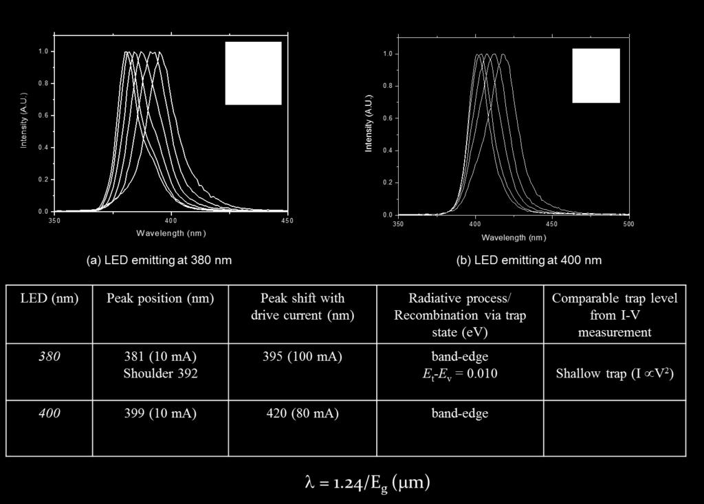
16 Electroluminescence Spectra
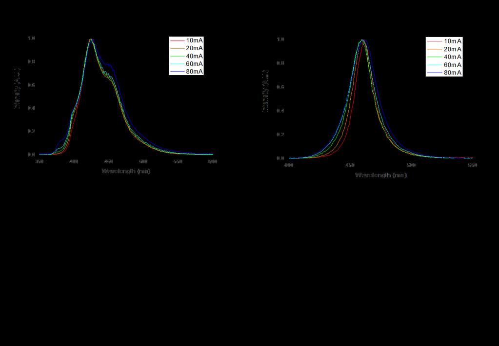
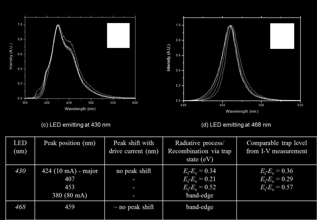
17 Electroluminescence Spectra Results
18 Emission Spectra from Blue LEDs: Effect of Deep States in the Spectra [Ref: Nana et al. Phys. Status Solidi A 207, (2010)]
19 Summary Gallium indium nitride based LEDs contributed high intensity monochromatic emission over the entire visible spectral range. White light sources have been obtained using suitable phosphors broadening emission peaks or multiple quantum wells with varying In content. The material system still contain deep level states that reduce emission efficiency. Conduction, particularly at low biases, occur through space charge limited current. LED based light sources are expected to dominate the general illumination field.
20 Acknowledgements Graduate students Saritha Akavaram, Okechukwu Akpa, Michael Awaah, Madhu Gowda, Arindra Guha, Alphonse Kamto, Roger Nana, Sahrukh Sakhawat, and Chelvi Parameswaran Auburn University Yaqi Wang and Minseo Park Research presented here was partially supported by NASA, Marshal Space flight Center and Glenn Research Center, Army Research Office, NSF - RISE, CREST, ERC (CIAN, University of Arizona) programs Power Point Slide Preparation Feline Agwumezie and Melvin DeBerry
Chapter 1 Overview of Semiconductor Materials and Physics
 Chapter 1 Overview of Semiconductor Materials and Physics Professor Paul K. Chu Conductivity / Resistivity of Insulators, Semiconductors, and Conductors Semiconductor Elements Period II III IV V VI 2 B
A semiconductor is an almost insulating material, in which by contamination (doping) positive or negative charge carriers can be introduced.
 positive or negative charge carriers can be introduced.") Semiconductor A semiconductor is an almost insulating material, in which by contamination (doping) positive or negative charge carriers can be introduced. Page 2 Semiconductor materials Page 3 Energy levels
Semiconductor A semiconductor is an almost insulating material, in which by contamination (doping) positive or negative charge carriers can be introduced. Page 2 Semiconductor materials Page 3 Energy levels
Electron Energy, E E = 0. Free electron. 3s Band 2p Band Overlapping energy bands. 3p 3s 2p 2s. 2s Band. Electrons. 1s ATOM SOLID.
 Electron Energy, E Free electron Vacuum level 3p 3s 2p 2s 2s Band 3s Band 2p Band Overlapping energy bands Electrons E = 0 1s ATOM 1s SOLID In a metal the various energy bands overlap to give a single
ρ ρ LED access resistances d A W d s n s p p p W the output window size p-layer d p series access resistance d n n-layer series access resistance
 LED access resistances W the output window size p-layer series access resistance d p n-layer series access resistance d n The n-layer series access resistance R = ρ s n where the resistivity of the n-layer
Lecture 7: Extrinsic semiconductors - Fermi level
 Lecture 7: Extrinsic semiconductors - Fermi level Contents 1 Dopant materials 1 2 E F in extrinsic semiconductors 5 3 Temperature dependence of carrier concentration 6 3.1 Low temperature regime (T < T
ELECTRONIC DEVICES AND CIRCUITS SUMMARY
 ELECTRONIC DEVICES AND CIRCUITS SUMMARY Classification of Materials: Insulator: An insulator is a material that offers a very low level (or negligible) of conductivity when voltage is applied. Eg: Paper,
Chapter 6: Light-Emitting Diodes
 Chapter 6: Light-Emitting Diodes Photoluminescence and electroluminescence Basic transitions Luminescence efficiency Light-emitting diodes Internal quantum efficiency External quantum efficiency Device
Quiz #1 Practice Problem Set
 Name: Student Number: ELEC 3908 Physical Electronics Quiz #1 Practice Problem Set? Minutes January 22, 2016 - No aids except a non-programmable calculator - All questions must be answered - All questions
Electronics The basics of semiconductor physics
 Electronics The basics of semiconductor physics Prof. Márta Rencz, Gergely Nagy BME DED September 16, 2013 The basic properties of semiconductors Semiconductors conductance is between that of conductors
Traps in MOCVD n-gan Studied by Deep Level Transient Spectroscopy and Minority Carrier Transient Spectroscopy
 Traps in MOCVD n-gan Studied by Deep Level Transient Spectroscopy and Minority Carrier Transient Spectroscopy Yutaka Tokuda Department of Electrical and Electronics Engineering, Aichi Institute of Technology,
Course overview. Me: Dr Luke Wilson. The course: Physics and applications of semiconductors. Office: E17 open door policy
 Course overview Me: Dr Luke Wilson Office: E17 open door policy email: luke.wilson@sheffield.ac.uk The course: Physics and applications of semiconductors 10 lectures aim is to allow time for at least one
Metal Vapour Lasers Use vapoured metal as a gain medium Developed by W. Silfvast (1966) Two types: Ionized Metal vapour (He-Cd) Neutral Metal vapour
 Two types: Ionized Metal vapour (He-Cd) Neutral Metal vapour") Metal Vapour Lasers Use vapoured metal as a gain medium Developed by W. Silfvast (1966) Two types: Ionized Metal vapour (He-Cd) Neutral Metal vapour (Cu) All operate by vaporizing metal in container Helium
Metal Vapour Lasers Use vapoured metal as a gain medium Developed by W. Silfvast (1966) Two types: Ionized Metal vapour (He-Cd) Neutral Metal vapour (Cu) All operate by vaporizing metal in container Helium
CME 300 Properties of Materials. ANSWERS: Homework 9 November 26, As atoms approach each other in the solid state the quantized energy states:
 CME 300 Properties of Materials ANSWERS: Homework 9 November 26, 2011 As atoms approach each other in the solid state the quantized energy states: are split. This splitting is associated with the wave
Schottky Rectifiers Zheng Yang (ERF 3017,
 ECE442 Power Semiconductor Devices and Integrated Circuits Schottky Rectifiers Zheng Yang (ERF 3017, email: yangzhen@uic.edu) Power Schottky Rectifier Structure 2 Metal-Semiconductor Contact The work function
Review of Semiconductor Fundamentals
 ECE 541/ME 541 Microelectronic Fabrication Techniques Review of Semiconductor Fundamentals Zheng Yang (ERF 3017, email: yangzhen@uic.edu) Page 1 Semiconductor A semiconductor is an almost insulating material,
PHYSICAL ELECTRONICS(ECE3540) CHAPTER 9 METAL SEMICONDUCTOR AND SEMICONDUCTOR HETERO-JUNCTIONS
 CHAPTER 9 METAL SEMICONDUCTOR AND SEMICONDUCTOR HETERO-JUNCTIONS") PHYSICAL ELECTRONICS(ECE3540) CHAPTER 9 METAL SEMICONDUCTOR AND SEMICONDUCTOR HETERO-JUNCTIONS Tennessee Technological University Monday, November 11, 013 1 Introduction Chapter 4: we considered the semiconductor
PHYSICAL ELECTRONICS(ECE3540) CHAPTER 9 METAL SEMICONDUCTOR AND SEMICONDUCTOR HETERO-JUNCTIONS Tennessee Technological University Monday, November 11, 013 1 Introduction Chapter 4: we considered the semiconductor
Chapter 7. Solar Cell
 Chapter 7 Solar Cell 7.0 Introduction Solar cells are useful for both space and terrestrial application. Solar cells furnish the long duration power supply for satellites. It converts sunlight directly
Lecture 9: Metal-semiconductor junctions
 Lecture 9: Metal-semiconductor junctions Contents 1 Introduction 1 2 Metal-metal junction 1 2.1 Thermocouples.......................... 2 3 Schottky junctions 4 3.1 Forward bias............................
Unit IV Semiconductors Engineering Physics
 Introduction A semiconductor is a material that has a resistivity lies between that of a conductor and an insulator. The conductivity of a semiconductor material can be varied under an external electrical
Semiconductor Devices and Circuits Fall Midterm Exam. Instructor: Dr. Dietmar Knipp, Professor of Electrical Engineering. Name: Mat. -Nr.
 Semiconductor Devices and Circuits Fall 2003 Midterm Exam Instructor: Dr. Dietmar Knipp, Professor of Electrical Engineering Name: Mat. -Nr.: Guidelines: Duration of the Midterm: 1 hour The exam is a closed
ET3034TUx Utilization of band gap energy
 ET3034TUx - 3.3.1 - Utilization of band gap energy In the last two weeks we have discussed the working principle of a solar cell and the external parameters that define the performance of a solar cell.
PHYSICAL ELECTRONICS(ECE3540) CHAPTER 9 METAL SEMICONDUCTOR AND SEMICONDUCTOR HETERO-JUNCTIONS
 CHAPTER 9 METAL SEMICONDUCTOR AND SEMICONDUCTOR HETERO-JUNCTIONS") PHYSICAL ELECTRONICS(ECE3540) CHAPTER 9 METAL SEMICONDUCTOR AND SEMICONDUCTOR HETERO-JUNCTIONS Tennessee Technological University Wednesday, October 30, 013 1 Introduction Chapter 4: we considered the
PHYSICAL ELECTRONICS(ECE3540) CHAPTER 9 METAL SEMICONDUCTOR AND SEMICONDUCTOR HETERO-JUNCTIONS Tennessee Technological University Wednesday, October 30, 013 1 Introduction Chapter 4: we considered the
MSE 310/ECE 340: Electrical Properties of Materials Fall 2014 Department of Materials Science and Engineering Boise State University
 MSE 310/ECE 340: Electrical Properties of Materials Fall 2014 Department of Materials Science and Engineering Boise State University Practice Final Exam 1 Read the questions carefully Label all figures
Introduction to Semiconductor Physics. Prof.P. Ravindran, Department of Physics, Central University of Tamil Nadu, India
 Introduction to Semiconductor Physics 1 Prof.P. Ravindran, Department of Physics, Central University of Tamil Nadu, India http://folk.uio.no/ravi/cmp2013 Review of Semiconductor Physics Semiconductor fundamentals
CLASS 12th. Semiconductors
 CLASS 12th Semiconductors 01. Distinction Between Metals, Insulators and Semi-Conductors Metals are good conductors of electricity, insulators do not conduct electricity, while the semiconductors have
Basic cell design. Si cell
 Basic cell design Si cell 1 Concepts needed to describe photovoltaic device 1. energy bands in semiconductors: from bonds to bands 2. free carriers: holes and electrons, doping 3. electron and hole current:
Spring Semester 2012 Final Exam
 Spring Semester 2012 Final Exam Note: Show your work, underline results, and always show units. Official exam time: 2.0 hours; an extension of at least 1.0 hour will be granted to anyone. Materials parameters
Semiconductor Junctions
 8 Semiconductor Junctions Almost all solar cells contain junctions between different materials of different doping. Since these junctions are crucial to the operation of the solar cell, we will discuss
Semiconductor. Byungwoo Park. Department of Materials Science and Engineering Seoul National University.
 Semiconductor Byungwoo Park Department of Materials Science and Engineering Seoul National University http://bp.snu.ac.kr http://bp.snu.ac.kr Semiconductors Kittel, Solid State Physics (Chapters 7 and
Metal Semiconductor Contacts
 Metal Semiconductor Contacts The investigation of rectification in metal-semiconductor contacts was first described by Braun [33-35], who discovered in 1874 the asymmetric nature of electrical conduction
February 1, 2011 The University of Toledo, Department of Physics and Astronomy SSARE, PVIC
 FUNDAMENTAL PROPERTIES OF SOLAR CELLS February 1, 2011 The University of Toledo, Department of Physics and Astronomy SSARE, PVIC Principles and Varieties of Solar Energy (PHYS 4400) and Fundamentals of
Sheng S. Li. Semiconductor Physical Electronics. Second Edition. With 230 Figures. 4) Springer
 Springer") Sheng S. Li Semiconductor Physical Electronics Second Edition With 230 Figures 4) Springer Contents Preface 1. Classification of Solids and Crystal Structure 1 1.1 Introduction 1 1.2 The Bravais Lattice
Sheng S. Li Semiconductor Physical Electronics Second Edition With 230 Figures 4) Springer Contents Preface 1. Classification of Solids and Crystal Structure 1 1.1 Introduction 1 1.2 The Bravais Lattice
Luminescence Process
 Luminescence Process The absorption and the emission are related to each other and they are described by two terms which are complex conjugate of each other in the interaction Hamiltonian (H er ). In an
David J. Starling Penn State Hazleton PHYS 214
 Being virtually killed by a virtual laser in a virtual space is just as effective as the real thing, because you are as dead as you think you are. -Douglas Adams, Mostly Harmless David J. Starling Penn
Schottky Diodes (M-S Contacts)
") Schottky Diodes (M-S Contacts) Three MITs of the Day Band diagrams for ohmic and rectifying Schottky contacts Similarity to and difference from bipolar junctions on electrostatic and IV characteristics.
Schottky Diodes (M-S Contacts) Three MITs of the Day Band diagrams for ohmic and rectifying Schottky contacts Similarity to and difference from bipolar junctions on electrostatic and IV characteristics.
Photonics and Optical Communication
 Photonics and Optical Communication (Course Number 300352) Spring 2007 Optical Source Dr. Dietmar Knipp Assistant Professor of Electrical Engineering http://www.faculty.iu-bremen.de/dknipp/ 1 Photonics
Engineering 2000 Chapter 8 Semiconductors. ENG2000: R.I. Hornsey Semi: 1
 Engineering 2000 Chapter 8 Semiconductors ENG2000: R.I. Hornsey Semi: 1 Overview We need to know the electrical properties of Si To do this, we must also draw on some of the physical properties and we
ECE 442. Spring, Lecture -2
 ECE 442 Power Semiconductor Devices and Integrated circuits Spring, 2006 University of Illinois at Chicago Lecture -2 Semiconductor physics band structures and charge carriers 1. What are the types of
1 Name: Student number: DEPARTMENT OF PHYSICS AND PHYSICAL OCEANOGRAPHY MEMORIAL UNIVERSITY OF NEWFOUNDLAND. Fall :00-11:00
 1 Name: DEPARTMENT OF PHYSICS AND PHYSICAL OCEANOGRAPHY MEMORIAL UNIVERSITY OF NEWFOUNDLAND Final Exam Physics 3000 December 11, 2012 Fall 2012 9:00-11:00 INSTRUCTIONS: 1. Answer all seven (7) questions.
Electrons are shared in covalent bonds between atoms of Si. A bound electron has the lowest energy state.
 Photovoltaics Basic Steps the generation of light-generated carriers; the collection of the light-generated carriers to generate a current; the generation of a large voltage across the solar cell; and
Review of Optical Properties of Materials
 Review of Optical Properties of Materials Review of optics Absorption in semiconductors: qualitative discussion Derivation of Optical Absorption Coefficient in Direct Semiconductors Photons When dealing
Recombination: Depletion. Auger, and Tunnelling
 Recombination: Depletion Region, Bulk, Radiative, Auger, and Tunnelling Ch 140 Lecture Notes #13 Prepared by David Gleason We assume: Review of Depletion Region Recombination Flat Quantum Fermi Levels
Lecture 2. Introduction to semiconductors Structures and characteristics in semiconductors
 Lecture 2 Introduction to semiconductors Structures and characteristics in semiconductors Semiconductor p-n junction Metal Oxide Silicon structure Semiconductor contact Literature Glen F. Knoll, Radiation
Semiconductor Device Physics
 1 Semiconductor Device Physics Lecture 1 http://zitompul.wordpress.com 2 0 1 3 2 Semiconductor Device Physics Textbook: Semiconductor Device Fundamentals, Robert F. Pierret, International Edition, Addison
EECS130 Integrated Circuit Devices
 EECS130 Integrated Circuit Devices Professor Ali Javey 8/30/2007 Semiconductor Fundamentals Lecture 2 Read: Chapters 1 and 2 Last Lecture: Energy Band Diagram Conduction band E c E g Band gap E v Valence
Basic Principles of Light Emission in Semiconductors
 Basic Principles of Light Emission in Semiconductors Class: Integrated Photonic Devices Time: Fri. 8:00am ~ 11:00am. Classroom: 資電 06 Lecturer: Prof. 李明昌 (Ming-Chang Lee) Model for Light Generation and
Carrier Transport Mechanisms of a-gaas/ n-si Heterojunctions
 Egypt. J. Sol., Vol. (24), No. (2), (2001) 245 Carrier Transport Mechanisms of a-gaas/ n-si Heterojunctions N.I.Aly, A.A.Akl, A.A.Ibrahim, and A.S.Riad Department of Physics, Faculty of Science, Minia
FIBER OPTICS. Prof. R.K. Shevgaonkar. Department of Electrical Engineering. Indian Institute of Technology, Bombay. Lecture: 12.
 FIBER OPTICS Prof. R.K. Shevgaonkar Department of Electrical Engineering Indian Institute of Technology, Bombay Lecture: 12 Optical Sources Fiber Optics, Prof. R.K. Shevgaonkar, Dept. of Electrical Engineering,
Introduction to Sources: Radiative Processes and Population Inversion in Atoms, Molecules, and Semiconductors Atoms and Molecules
 OPTI 500 DEF, Spring 2012, Lecture 2 Introduction to Sources: Radiative Processes and Population Inversion in Atoms, Molecules, and Semiconductors Atoms and Molecules Energy Levels Every atom or molecule
PHYSICS nd TERM Outline Notes (continued)
") PHYSICS 2800 2 nd TERM Outline Notes (continued) Section 6. Optical Properties (see also textbook, chapter 15) This section will be concerned with how electromagnetic radiation (visible light, in particular)
PHYSICS 2800 2 nd TERM Outline Notes (continued) Section 6. Optical Properties (see also textbook, chapter 15) This section will be concerned with how electromagnetic radiation (visible light, in particular)
Simulation of GaN-based Light-Emitting Devices
 Simulation of GaN-based Light-Emitting Devices Joachim Piprek Solid-State Lighting and Display Center Materials Department, College of Engineering University of California, Santa Barbara, CA 93106 piprek@ieee.org
Figure 3.1 (p. 141) Figure 3.2 (p. 142)
 Figure 3.2 (p. 142)") Figure 3.1 (p. 141) Allowed electronic-energy-state systems for two isolated materials. States marked with an X are filled; those unmarked are empty. System 1 is a qualitative representation of a metal;
Figure 3.1 (p. 141) Allowed electronic-energy-state systems for two isolated materials. States marked with an X are filled; those unmarked are empty. System 1 is a qualitative representation of a metal;
Lecture 1. OUTLINE Basic Semiconductor Physics. Reading: Chapter 2.1. Semiconductors Intrinsic (undoped) silicon Doping Carrier concentrations
 silicon Doping Carrier concentrations") Lecture 1 OUTLINE Basic Semiconductor Physics Semiconductors Intrinsic (undoped) silicon Doping Carrier concentrations Reading: Chapter 2.1 EE105 Fall 2007 Lecture 1, Slide 1 What is a Semiconductor? Low
Lecture 1 OUTLINE Basic Semiconductor Physics Semiconductors Intrinsic (undoped) silicon Doping Carrier concentrations Reading: Chapter 2.1 EE105 Fall 2007 Lecture 1, Slide 1 What is a Semiconductor? Low
Semiconductors and Optoelectronics. Today Semiconductors Acoustics. Tomorrow Come to CH325 Exercises Tours
 Semiconductors and Optoelectronics Advanced Physics Lab, PHYS 3600 Don Heiman, Northeastern University, 2017 Today Semiconductors Acoustics Tomorrow Come to CH325 Exercises Tours Semiconductors and Optoelectronics
ELEC 4700 Assignment #2
 ELEC 4700 Assignment #2 Question 1 (Kasop 4.2) Molecular Orbitals and Atomic Orbitals Consider a linear chain of four identical atoms representing a hypothetical molecule. Suppose that each atomic wavefunction
Semiconductor device structures are traditionally divided into homojunction devices
 0. Introduction: Semiconductor device structures are traditionally divided into homojunction devices (devices consisting of only one type of semiconductor material) and heterojunction devices (consisting
Laser Basics. What happens when light (or photon) interact with a matter? Assume photon energy is compatible with energy transition levels.
 interact with a matter? Assume photon energy is compatible with energy transition levels.") What happens when light (or photon) interact with a matter? Assume photon energy is compatible with energy transition levels. Electron energy levels in an hydrogen atom n=5 n=4 - + n=3 n=2 13.6 = [ev]
What happens when light (or photon) interact with a matter? Assume photon energy is compatible with energy transition levels. Electron energy levels in an hydrogen atom n=5 n=4 - + n=3 n=2 13.6 = [ev]
Chapter 5. Semiconductor Laser
 Chapter 5 Semiconductor Laser 5.0 Introduction Laser is an acronym for light amplification by stimulated emission of radiation. Albert Einstein in 1917 showed that the process of stimulated emission must
PHOTOVOLTAICS Fundamentals
 PHOTOVOLTAICS Fundamentals PV FUNDAMENTALS Semiconductor basics pn junction Solar cell operation Design of silicon solar cell SEMICONDUCTOR BASICS Allowed energy bands Valence and conduction band Fermi
1 Review of semiconductor materials and physics
 Part One Devices 1 Review of semiconductor materials and physics 1.1 Executive summary Semiconductor devices are fabricated using specific materials that offer the desired physical properties. There are
EE 6313 Homework Assignments
 EE 6313 Homework Assignments 1. Homework I: Chapter 1: 1.2, 1.5, 1.7, 1.10, 1.12 [Lattice constant only] (Due Sept. 1, 2009). 2. Homework II: Chapter 1, 2: 1.17, 2.1 (a, c) (k = π/a at zone edge), 2.3
OPTICAL RESPONSE STUDY OF THE Al=a-SiC:H SCHOTTKY DIODE FOR DIFFERENT SUBSTRATE TEMPERATURES OF THE r.f. SPUTTERED a-sic:h THIN FILM
 Active and Passive Elec. Comp., 2003, Vol. 26(2), pp. 63 70 OPTICAL RESPONSE STUDY OF THE Al=a-SiC:H SCHOTTKY DIODE FOR DIFFERENT SUBSTRATE TEMPERATURES OF THE r.f. SPUTTERED a-sic:h THIN FILM L. MAGAFAS
Schottky diodes. JFETs - MESFETs - MODFETs
 Technische Universität Graz Institute of Solid State Physics Schottky diodes JFETs - MESFETs - MODFETs Quasi Fermi level When the charge carriers are not in equilibrium the Fermi energy can be different
Lecture 2. Introduction to semiconductors Structures and characteristics in semiconductors. Fabrication of semiconductor sensor
 Lecture 2 Introduction to semiconductors Structures and characteristics in semiconductors Semiconductor p-n junction Metal Oxide Silicon structure Semiconductor contact Fabrication of semiconductor sensor
n N D n p = n i p N A
 Summary of electron and hole concentration in semiconductors Intrinsic semiconductor: E G n kt i = pi = N e 2 0 Donor-doped semiconductor: n N D where N D is the concentration of donor impurity Acceptor-doped
Conductivity and Semi-Conductors
 Conductivity and Semi-Conductors J = current density = I/A E = Electric field intensity = V/l where l is the distance between two points Metals: Semiconductors: Many Polymers and Glasses 1 Electrical Conduction
Technological Status of UVALED Techniques Application in Magnetic Particle and Penetrant Inspection
 11th European Conference on Non-Destructive Testing (ECNDT 2014), October 6-10, 2014, Prague, Czech Republic More Info at Open Access Database www.ndt.net/?id=16474 Technological Status of UVALED Techniques
EE 130 Intro to MS Junctions Week 6 Notes. What is the work function? Energy to excite electron from Fermi level to the vacuum level
 EE 13 Intro to S Junctions eek 6 Notes Problem 1 hat is the work function? Energy to ecite electron from Fermi level to the vacuum level Electron affinity of 4.5eV Electron affinity of Ge 4.eV orkfunction
Lecture 2. Introduction to semiconductors Structures and characteristics in semiconductors
 Lecture 2 Introduction to semiconductors Structures and characteristics in semiconductors Semiconductor p-n junction Metal Oxide Silicon structure Semiconductor contact Literature Glen F. Knoll, Radiation
Emission Spectra of the typical DH laser
 Emission Spectra of the typical DH laser Emission spectra of a perfect laser above the threshold, the laser may approach near-perfect monochromatic emission with a spectra width in the order of 1 to 10
Introduction to Optoelectronic Device Simulation by Joachim Piprek
 NUSOD 5 Tutorial MA Introduction to Optoelectronic Device Simulation by Joachim Piprek Outline:. Introduction: VCSEL Example. Electron Energy Bands 3. Drift-Diffusion Model 4. Thermal Model 5. Gain/Absorption
UNIVERSITY OF CALIFORNIA College of Engineering Department of Electrical Engineering and Computer Sciences. EECS 130 Professor Ali Javey Fall 2006
 UNIVERSITY OF CALIFORNIA College of Engineering Department of Electrical Engineering and Computer Sciences EECS 130 Professor Ali Javey Fall 2006 Midterm I Name: Closed book. One sheet of notes is allowed.
GaN for use in harsh radiation environments
 4 th RD50 - Workshop on radiation hard semiconductor devices for very high luminosity colliders GaN for use in harsh radiation environments a (W Cunningham a, J Grant a, M Rahman a, E Gaubas b, J Vaitkus
Luminescence basics. Slide # 1
 Luminescence basics Types of luminescence Cathodoluminescence: Luminescence due to recombination of EHPs created by energetic electrons. Example: CL mapping system Photoluminescence: Luminescence due to
UNIT I: Electronic Materials.
 SIDDHARTH INSTITUTE OF ENGINEERING & TECHNOLOGY :: PUTTUR Siddharth Nagar, Narayanavanam Road 517583 QUESTION BANK (DESCRIPTIVE) Subject with Code: SEMICONDUCTOR PHYSICS (18HS0851) Course & Branch: B.Tech
Introductory Nanotechnology ~ Basic Condensed Matter Physics ~
 Introductory Nanotechnology ~ Basic Condensed Matter Physics ~ Atsufumi Hirohata Department of Electronics Quick Review over the Last Lecture Classic model : Dulong-Petit empirical law c V, mol 3R 0 E
Current mechanisms Exam January 27, 2012
 Current mechanisms Exam January 27, 2012 There are four mechanisms that typically cause currents to flow: thermionic emission, diffusion, drift, and tunneling. Explain briefly which kind of current mechanisms
Classification of Solids
 Classification of Solids Classification by conductivity, which is related to the band structure: (Filled bands are shown dark; D(E) = Density of states) Class Electron Density Density of States D(E) Examples
ELECTRONIC I Lecture 1 Introduction to semiconductor. By Asst. Prof Dr. Jassim K. Hmood
 ELECTRONIC I Lecture 1 Introduction to semiconductor By Asst. Prof Dr. Jassim K. Hmood SOLID-STATE ELECTRONIC MATERIALS Electronic materials generally can be divided into three categories: insulators,
Semi-Conductor & Diodes
 Semi-Conductor & Diodes Semi-Conductor Some Quantum mechanics refresher Band theory in solids: Semiconductor, insulator and conductor Doping Diode p-n junction Diode types applications Introduction In
8. Schottky contacts / JFETs
 Technische Universität Graz Institute of Solid State Physics 8. Schottky contacts / JFETs Nov. 21, 2018 Technische Universität Graz Institute of Solid State Physics metal - semiconductor contacts Photoelectric
Photonic Devices. Light absorption and emission. Transitions between discrete states
 Light absorption and emission Photonic Devices Transitions between discrete states Transition rate determined by the two states: Fermi s golden rule Absorption and emission of a semiconductor Vertical
Self-Assembled InAs Quantum Dots
 Self-Assembled InAs Quantum Dots Steve Lyon Department of Electrical Engineering What are semiconductors What are semiconductor quantum dots How do we make (grow) InAs dots What are some of the properties
OPTI510R: Photonics. Khanh Kieu College of Optical Sciences, University of Arizona Meinel building R.626
 OPTI510R: Photonics Khanh Kieu College of Optical Sciences, University of Arizona kkieu@optics.arizona.edu Meinel building R.626 Announcements HW#3 is assigned due Feb. 20 st Mid-term exam Feb 27, 2PM
R. Ludwig and G. Bogdanov RF Circuit Design: Theory and Applications 2 nd edition. Figures for Chapter 6
 R. Ludwig and G. Bogdanov RF Circuit Design: Theory and Applications 2 nd edition Figures for Chapter 6 Free electron Conduction band Hole W g W C Forbidden Band or Bandgap W V Electron energy Hole Valence
Semiconductor Physical Electronics
 Semiconductor Physical Electronics Sheng S. Li Department of Electrical Engineering University of Florida Gainesville, Florida Plenum Press New York and London Contents CHAPTER 1. Classification of Solids
EE301 Electronics I , Fall
 EE301 Electronics I 2018-2019, Fall 1. Introduction to Microelectronics (1 Week/3 Hrs.) Introduction, Historical Background, Basic Consepts 2. Rewiev of Semiconductors (1 Week/3 Hrs.) Semiconductor materials
KATIHAL FİZİĞİ MNT-510
 KATIHAL FİZİĞİ MNT-510 YARIİLETKENLER Kaynaklar: Katıhal Fiziği, Prof. Dr. Mustafa Dikici, Seçkin Yayıncılık Katıhal Fiziği, Şakir Aydoğan, Nobel Yayıncılık, Physics for Computer Science Students: With
Comparison of Ge, InGaAs p-n junction solar cell
 ournal of Physics: Conference Series PAPER OPEN ACCESS Comparison of Ge, InGaAs p-n junction solar cell To cite this article: M. Korun and T. S. Navruz 16. Phys.: Conf. Ser. 77 135 View the article online
Review Energy Bands Carrier Density & Mobility Carrier Transport Generation and Recombination
 Review Energy Bands Carrier Density & Mobility Carrier Transport Generation and Recombination The Metal-Semiconductor Junction: Review Energy band diagram of the metal and the semiconductor before (a)
Theory of Electrical Characterization of Semiconductors
 Theory of Electrical Characterization of Semiconductors P. Stallinga Universidade do Algarve U.C.E.H. A.D.E.E.C. OptoElectronics SELOA Summer School May 2000, Bologna (It) Overview Devices: bulk Schottky
Session 6: Solid State Physics. Diode
 Session 6: Solid State Physics Diode 1 Outline A B C D E F G H I J 2 Definitions / Assumptions Homojunction: the junction is between two regions of the same material Heterojunction: the junction is between
Section 12: Intro to Devices
 Section 12: Intro to Devices Extensive reading materials on reserve, including Robert F. Pierret, Semiconductor Device Fundamentals Bond Model of Electrons and Holes Si Si Si Si Si Si Si Si Si Silicon
ISSN Review. Progress to a Gallium-Arsenide Deep-Center Laser
 Materials 2009, 2, 1599-1635; doi:10.3390/ma2041599 OPEN ACCESS materials ISSN 1996-1944 www.mdpi.com/journal/materials Review Progress to a Gallium-Arsenide Deep-Center Laser Janet L. Pan Yale University,
Chapter Two. Energy Bands and Effective Mass
 Chapter Two Energy Bands and Effective Mass Energy Bands Formation At Low Temperature At Room Temperature Valence Band Insulators Metals Effective Mass Energy-Momentum Diagrams Direct and Indirect Semiconduction
Lecture 1. Introduction to Electronic Materials. Reading: Pierret 1.1, 1.2, 1.4,
 Lecture 1 Introduction to Electronic Materials Reading: Pierret 1.1, 1.2, 1.4, 2.1-2.6 Atoms to Operational Amplifiers The goal of this course is to teach the fundamentals of non-linear circuit elements
EECS143 Microfabrication Technology
 EECS143 Microfabrication Technology Professor Ali Javey Introduction to Materials Lecture 1 Evolution of Devices Yesterday s Transistor (1947) Today s Transistor (2006) Why Semiconductors? Conductors e.g
Simulation of AlGaN/Si and InN/Si ELECTRIC DEVICES
 Simulation of AlGaN/Si and InN/Si ELECTRIC DEVICES Zehor Allam 1, Abdelkader Hamdoune 2, Chahrazed Boudaoud 3, Asmaa Amrani 4,Aicha Soufi 5,Zakia Nakoul 6 Unity of Research Materials and Renewable Energies,
Hussein Ayedh. PhD Studet Department of Physics
 Hussein Ayedh PhD Studet Department of Physics OUTLINE Introduction Semiconductors Basics DLTS Theory DLTS Requirements Example Summary Introduction Energetically "deep trapping levels in semiconductor
Semiconductor Physics Problems 2015
 Semiconductor Physics Problems 2015 Page and figure numbers refer to Semiconductor Devices Physics and Technology, 3rd edition, by SM Sze and M-K Lee 1. The purest semiconductor crystals it is possible