Noisy dynamics in nanoelectronic systems. Technische Physik, Universität Würzburg, Germany
|
|
|
- Darcy Berry
- 5 years ago
- Views:
Transcription


1 Noisy dynamics in nanoelectronic systems Lukas Worschech Technische Physik, Universität Würzburg, Germany
2 Team Transport: FH F. Hartmann, SK S. Kremling, S. SGöpfert, L. LGammaitoni i Technology: M. Emmerling, S. Kuhn, T. Steinl, M. Kamp III V samples: III-V samples: C. Schneider, S. Höfling
3 Motivation: Stochastic resonance (SR), a noise enhanced information transfer process Stochastic resonance: Weak signals can be enhanced by fluctuations (for a review Ref.[1]) Ingredients: Noise Sub-threshold signal Non-linear system, e.g. bistable systems SR as model was introduced to explain the periodic recurrences of ice ages: Benzi, Parisi, i Sutera, Vulpiani [] SR has been found in various systems, e.g. in crayfish mechanoreceptors [3] [1] L. Gammaitoni et al., Stochastic resonance, Reviews of Modern Physics, Vol. 70, No. 1, January 1998 [] Benzi, R., G. Parisi, A. Sutera, and A. Vulpiani, 198, Tellus 34, 10. [3] Douglass, J. K., L. Wilkens, E. Pantazelou, and F. Moss, 1993, Nature (London) 365, 337.
4 Outline Nanoelectronic semiconductor electronic devices Technology Mesoscopic devices Nonlinear transport BL Motors Y-branch switch as half adder Quantum dot as a memory Resonant tunneling diode: Sensor, logic stochastic resonance Best detection strategy
5 Outline Nanoelectronic semiconductor electronic devices Technology Mesoscopic devices Nonlinear transport BL Motors Y-branch switch as half adder Quantum dot as a memory Resonant tunneling diode: Sensor, logic stochastic resonance Best detection strategy
6 semiconductors Electronics: frequencies Hz THz Optoelectronics: wavelengths µm
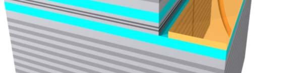
7 Heterostructures: Band gap engineering Combination of different semiconductors with atomic precision Growth techniques: e.g. Molecular beam epitaxy (MBE)


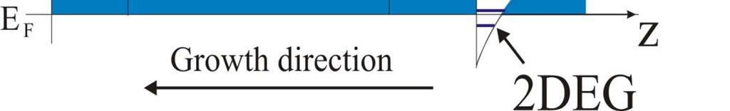
8 GaAs/AlGaAs HEMT Modulation-doped GaAs/AlGaAs heterostruktur (HEMT) Mean free path: 4,K / 50 RT


9 Structuring Top-down route: lithography, etching, Bottom-up route: self-assembly, seeded growth, Different geometries: wires, dots, rings, splitters
10 Outline Nanoelectronic semiconductor electronic devices Technology Mesoscopic devices Nonlinear transport BL Motors Y-branch switch as half adder Quantum dot as a memory Resonant tunneling diode: Sensor, logic stochastic resonance Best detection strategy
11 Characteristic lengths De Broglie wavelength: l debroglie h / p Fermi wavelength: l F l debroglie E E F p k k e k k Mean free path: l m v m e m e Phase coherence length: l h / mkt L a) Diffusive b) Coherent c) Ballistic a) b) c) W


12 Linear mesoscopic transport p p Conductance quantization in 1D wires 1D wires I I I L R R L T T f f E E de h e ev f R L D v D * * *1/ ) ( ~ 1 ev ) ( ~ T h e V I G / Multi-terminal conductor: h Landauer-Büttiker formula j ij i i T e I j j ij i i T h I

.")


 n = 3.")
13 What is nano? A comparison: metals vs semiconductor H. Ohnishi et al., Nature 395, (1998). Metal: Gold film n =.3 x /cm l F = 0.5 nm, E F =5.5 ev l m ~ nm l ~ m Semiconductor: dimensional electron gas (DEG) n = 3.0 x /cm l F = 46 nm, E F = 11 mev l m ~ m T < 4 K l ~ m
 7 6 5 4 3 1 0-1 0,5 1,0 1,5 V g")
14 Quantum wire Electron wave propagation: each occupied subband contributes with e /h to the conductance 8 conductance quantization G (e /h) ,5 1,0 1,5 V g (V)
=G(-B) G(e /h 4, 4,0 ~ 3,8 3,6 h) 3,4 3, 3,0 A( r) dr h f r 59(0) nm e,8-0,06-0,04-0,0 0,00 0,0 0,04 0,06")
15 Quantum ring Quantum oscillations: Aharonov-Bohm effect Magnetic field symmetry in linear mesocopic transport G(B)=G(-B) G(e /h 4, 4,0 ~ 3,8 3,6 h) 3,4 3, 3,0 A( r) dr h f r 59(0) nm e,8-0,06-0,04-0,0 0,00 0,0 0,04 0,06 B(T)
16 Conductor with 3 contacts 1 S S Current conservation symmetry 1 S S ij s ji s ij s ij T 1 r G G r Transmission matrix r r r G r r G G r G r r G G r r G G r G G r T Switching parameter 1 1 r r ), ( 1 V V G g I-V curve 1 1 V V T I h e I I 3 3 V h I
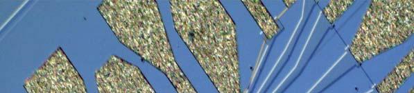
17 Y-branch switch Stem and branches controlled by side gates
18 Non-linear transport via interaction Mesoscopic capacitance: Self-switching in a YBS 1 qd qg 1 Dqd / Cgd Dqd / Dqg C g b C D D b b g C D C lr b g C b lr g
 1.50 1.")
 Push-pull Mode: V")
 0.00-0. -0.1 0.0 0.")
19 YBS V bias = 1.75 V 1.00 V 0.50 V V bl (V) V br (V) Push-pull Mode: V gl + V gr = const (dv gl = -dv gr ) V g (V)
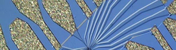
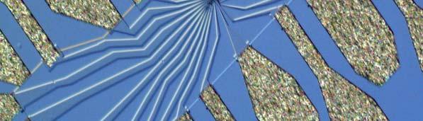
20 Dynamical gate operation in a YBS
21 Outline Nanoelectronic semiconductor electronic devices Technology Mesoscopic devices Nonlinear transport BL Motors Y-branch switch as half adder Quantum dot as a memory Resonant tunneling diode: Sensor, logic stochastic resonance Best detection strategy
22 Solar cell absorption rectifier Optical excitation of electron hole pair Separation by a p-n junction: asymmetry in the device structure Is it possible to generate a current in a symmetric structure?
23 Yes! If the nonlinear noise is asymmetric: Transport as a consequence of state-dependent diffusion Diffusion constants: Double well potential with minima located at A and D. D is the energetic favorable point D with D < A. Consider two temperatures at the slopes T hot and T cold with T hot >T cold. For systems subject to thermal noise, the Boltzmann factor is V exp( ) kt M. Büttiker, Z. Phys. B 68, 161 (1987). R. Landauer, J. Stat. Phys. 53, 33 (1988). For systems with mobility µ subject to drift and state dependent diffusion the Boltzmann factor is with exp( (q))
. Ya. M. Blanter and M.")
sin( ) T 0 1 0 0 I With: T E0 exp(")
24 Transport as a consequence of state-dependent diffusion M. Büttiker, Z. Phys. B 68, 161 (1987). Ya. M. Blanter and M. Büttiker, Phys. Rev. Lett. 81, (1998). I ov E T L T E 0 exp( )sin( ) T I With: T E0 exp( )sin( ) T 1 mt 0 0
25 Outline Nanoelectronic semiconductor electronic devices Technology Mesoscopic devices Nonlinear transport BL Motors Y-branch switch as half adder Quantum dot as a memory Resonant tunneling diode: Sensor, logic stochastic resonance Best detection strategy
26 Y-branch as ballistic rectification Rectification due to junctions: pn-junction Metal-semiconductor junction Y-branch junction: no geometrical asymmetry! V (Y) r 0,00 V l (X) V s (X AND Y) V r V s (V) -0, ,10 V s -0,15 Experiment Theory: diffusive ballistic -0,4-0, 0,0 0, 0,4 V l V xy (V)

 -0,10")

27 Y-branch as ballistic rectification diffusive Transport V l V r 0,00-0,05 V s (V) -0,10 Quasi-ballistic Transport -0,15 diffusive ballistic V s -0,4 0,0 0,4 V xy (V)
28 YBS nonlinearity used for a compact adder Half-Adder: binary addition with carry bit Truth table X Y Z C H H L H Sh Scheme X & = AND Y & C = = XOR H L H L L H H L = Z L L L L > 10 FETs + interconnects t


29 Nanoelectronic Half-Adder planar Half-Adder is based on ballistic Y-junctions Inputs: x and y x g Outputs: c and z Working point: s Control: v v y c l z r 100 nm s L. Worschech et al., Appl. Phys. Lett. 83, 46 (003)
30 Model control of V z via V c : gate a) Injection of electrons l r s b) Gating No external gate! V c c R z V s V z Self induced switching V d
31 V g Demonstration o of logic ogc function at RT: V x x V y y c z y c z V c l R V d r V z s V s z (V) V z 0,10 0,00 T = 4. K T = 50 K T = 300 K -0,10 X Y Z C H H L H H L H L L H H L V c (V) 000 0,00-0,5-0,50-0,75 (HH) (LH) (HL) (LL) (HH) (LH) (HL) (LL) L L L L Logic inputs (XY) (HH) (LH) (HL) (LL)
32 Outline Nanoelectronic semiconductor electronic devices Technology Mesoscopic devices Nonlinear transport BL Motors Y-branch switch as half adder Quantum dot as a memory Resonant tunneling diode: Sensor, logic stochastic resonance Best detection strategy

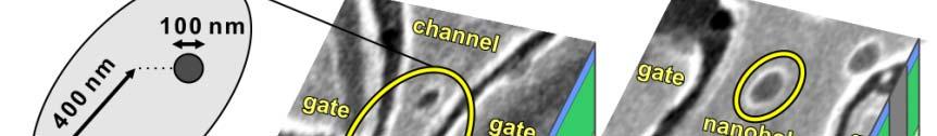
33 Positioned QDs


 Coulomb")


34 SET by positioning of QDs in a wire M. Stopa, Harvard 0,0 G/G 0 0, ,00 0,3 0,4 0,5 0,6 0,7 0,8 0,9 1,0 1,1 1, V g (V) Coulomb oscillations due to charging of island with single electrons Coulomb-Diamond used to extract capacitances, charging energy > 10 mev
 Schaltspannung V W V g CWq 1 C g Q Cgq C C Wq")
35 Memory: threshold shift of read-out transistor 7,5 5,0,5 0,0 17,5 V th I d (A A) 15,0 1,5 10,0 7,5 5,0,5 0, V g (V) Schaltspannung V W V g CWq 1 C g Q Cgq C C Wq gq
36 Outline Nanoelectronic semiconductor electronic devices Technology Mesoscopic devices Nonlinear transport BL Motors Y-branch switch as half adder Quantum dot as a memory Resonant tunneling diode: Sensor, logic stochastic resonance Best detection strategy


37 Resonant-tunneling diode fast operation ~THz negative differential resistance ballistic operation at room temperature
38 RTD operation
39 Logic operation with RTD mesas V (mv) split RTD diameter: 600nm 0,00 0,5 0,50 0,75 1,00 1,5 1,50 V dc (V)
40 Noise-activated switching Ultra-miniaturized circuits: Small signal-to-noise ratios (SNR) & feedback between different devices are unavoidable Subtle strategy: exploit ambient noise and feedback action for electronic applications


41 No thermal transconductance limit ultra small switching voltages
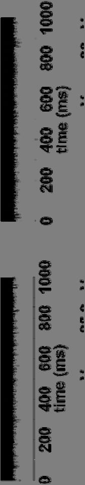
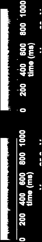
42 Logic RTD gates V ac = 3 mv V ac = 4.5 mv V ac = 5 mv V 1 = V = 0 mv == Log. input I = I 1 +I =0+0=0


43 Logic RTD gates V ac = 5 mv V ac = 6 mv V ac = 6.5 mv V 1 = 0, V =,0 mv == Log. input I = I 1 +I =1+0=0+1=1

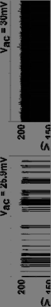
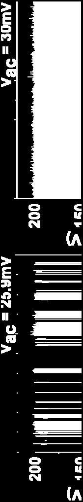
44 Logic RTD gates V ac = 6.5 mv V ac = 7.5 mv V ac = 9 mv V 1 = V = mv == Log. input I = I 1 +I =1+1=


45 Logic RTD gates NOR NAND transition from NOR to NAND opertation for amplitude changes smaller than 1 mv


. L. W., F. Hartmann,T. Y.")

46 Logic stochastic resonance Murali, K., Sinha, S., Ditto, W., Bulsara, A. Phys. Rev. Lett. 10, (009). Murali, K., Rajamohamed, I., Sinha, S., Ditto, W., and Bulsara, A., Appl. Phys. Lett. 95, (009). L. W., F. Hartmann,T. Y. Kim,S. Höfling,M. Kamp,A. Forchel,J. Ahopelto,I. Neri,A. Dari, L. Gammaitoni, APL 010
47 Stochastic resonance : A short introduction L. Gammaitoni et al., Stochastic resonance, Reviews of Modern Physics, Vol. 70, No. 1, January 1998 Overdamped motion of a Brownian particle in a bistable potential in the presence of noise and periodic forcing. with x V `( x) A0 V 1 cos( t ) ( t) ( x) x x Noise-induced hopping between the local equilibrium states with the Kramers rate 1 V r K exp( D The time-scale matching condition for stochastic resonance: T T K )


48 Stochastic resonance in resonant tunneling diodes: Exploiting noise & nonlinearity RTD is bistable with stable outputs I H = 800 µa and I L = 70 µa. RT PVR ~ 3 Noise induced switching between the two stable states appear. Time scale T k is given by the inverse of the Kramer s rate.


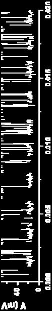
49 Recording of SR: Spectral response <V> versus the noise power added to the device For P noise <P SR no spectral component at f = 500 Hz is found. For P noise > P SR the spectral component at f = 500 Hz is still apparent. At the optimum noise level P SR, the spectral amplitude reaches a maximum value and is decreasing apart from P SR.


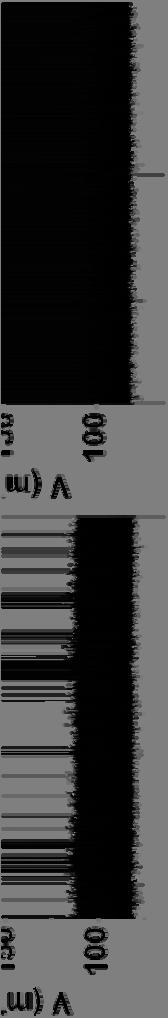
50 Stochastic resonance: Time trace signals P noise = nw P noise = 3 nw noise P noise = 11 nw At P noise = 3 nw the output follows almost perfectly the input signal!!


 V g 0 V")
51 YBS: Residence time magnetic field detector The input and the working point voltages set the condition of the Y-branch switch. Self-gating leads to a bistable transfer characteristic. Noise induced oscillations occur All 0K. Input signal: V g ( t) V g 0 V sin( ), g t Weak periodic signal: V g mV


52 Magnetic field sensors based on the residence time difference in electron waveguides The detector in biased in the strongly noise activated regime. Switching between V H and V L solely controlled by the internal noise. Magnetic field is applied perpendicular to the motion of electrons. Measure the time spent in each of the two stable states: n H, L 1 T H T H, L nh, L i1 T T H i, L Output of the detector is the residence time difference: T H T L i
53 Vb br (V) Magnetic field sensors based on the residence time difference in electron waveguides V br,th Vbarrier (V) ,50-0, , , , B B th -0, B (T) The magnetic-field induced switching (between V H and V L ) is associated with an interplay between a scattering asymmetry at the boundaries. [1] Increasing magnetic field: The output V br decreases linearly down to a magnetic field threshold B th. Transitions between the two stable states occur within a magnetic field range B. The output V br changed its stable state from V br = V H to V br = V L. Vbr r,th (V) [1] D. Hartmann et al., PHYSICAL REVIEW B 78, (008) Vbarrier (V) Bth B (T)
54 mean res sidence ti ime (s) Magnetic field sensors based on the residence time difference in electron waveguides.0 TH TL B (mt) T (s) 1.5 Measurement 1.0 Simulation Linear Fit B (mt) The residence time T H (high state) is decreasing and T L (low state) is increasing with increasing B. Output T is a linear function of the magnetic field around the symmetric point T = 0 s. Target signal (magnetic field) independent sensitivity. T ( B) T0 cb T S ( B) c B
Energy harvesting in nanoelectronic devices. Technische Physik, Universität Würzburg, Germany
 Energy harvesting in nanoelectronic devices Lukas Worschech Technische Physik, Universität Würzburg, Germany Energy harvesting with nanoelectronics Energy harvesting: Energy provider+transducer+rectifier
Nano-electronic Stochastic Logic Gates - Memory Devices - Sensors and Energy Harvester
 Nano-electronic Stochastic Logic Gates - Memory Devices - Sensors and Energy Harvester F. Hartmann 1, A. Pfenning 1, P. Maier 1, P. Pfeffer 1, I.Neri 2, A. Forchel 1, L. Gammaitoni 2 and L. Worschech 1
single-electron electron tunneling (SET)
") single-electron electron tunneling (SET) classical dots (SET islands): level spacing is NOT important; only the charging energy (=classical effect, many electrons on the island) quantum dots: : level spacing
single-electron electron tunneling (SET) classical dots (SET islands): level spacing is NOT important; only the charging energy (=classical effect, many electrons on the island) quantum dots: : level spacing
Introduction to semiconductor nanostructures. Peter Kratzer Modern Concepts in Theoretical Physics: Part II Lecture Notes
 Introduction to semiconductor nanostructures Peter Kratzer Modern Concepts in Theoretical Physics: Part II Lecture Notes What is a semiconductor? The Fermi level (chemical potential of the electrons) falls
QUANTUM INTERFERENCE IN SEMICONDUCTOR RINGS
 QUANTUM INTERFERENCE IN SEMICONDUCTOR RINGS PhD theses Orsolya Kálmán Supervisors: Dr. Mihály Benedict Dr. Péter Földi University of Szeged Faculty of Science and Informatics Doctoral School in Physics
PHYSICS OF NANOSTRUCTURES
 PHYSICS OF NANOSTRUCTURES Proceedings of the Thirty-Eighth Scottish Universities Summer School in Physics, St Andrews, July-August 1991. A NATO Advanced Study Institute. Edited by J H Davies Glasgow University
Nanoelectronics. Topics
 Nanoelectronics Topics Moore s Law Inorganic nanoelectronic devices Resonant tunneling Quantum dots Single electron transistors Motivation for molecular electronics The review article Overview of Nanoelectronic
Electronic transport in low dimensional systems
 Electronic transport in low dimensional systems For example: 2D system l
Physics and Material Science of Semiconductor Nanostructures
 Physics and Material Science of Semiconductor Nanostructures PHYS 570P Prof. Oana Malis Email: omalis@purdue.edu Course website: http://www.physics.purdue.edu/academic_programs/courses/phys570p/ 1 Introduction
Quantum physics in quantum dots
 Quantum physics in quantum dots Klaus Ensslin Solid State Physics Zürich AFM nanolithography Multi-terminal tunneling Rings and dots Time-resolved charge detection Moore s Law Transistors per chip 10 9
Quantum-Effect and Single-Electron Devices
 368 IEEE TRANSACTIONS ON NANOTECHNOLOGY, VOL. 2, NO. 4, DECEMBER 2003 Quantum-Effect and Single-Electron Devices Stephen M. Goodnick, Fellow, IEEE, and Jonathan Bird, Senior Member, IEEE Abstract In this
Terahertz sensing and imaging based on carbon nanotubes:
 Terahertz sensing and imaging based on carbon nanotubes: Frequency-selective detection and near-field imaging Yukio Kawano RIKEN, JST PRESTO ykawano@riken.jp http://www.riken.jp/lab-www/adv_device/kawano/index.html
Surfaces, Interfaces, and Layered Devices
 Surfaces, Interfaces, and Layered Devices Building blocks for nanodevices! W. Pauli: God made solids, but surfaces were the work of Devil. Surfaces and Interfaces 1 Interface between a crystal and vacuum
Chapter 3 Properties of Nanostructures
 Chapter 3 Properties of Nanostructures In Chapter 2, the reduction of the extent of a solid in one or more dimensions was shown to lead to a dramatic alteration of the overall behavior of the solids. Generally,
Quantum Phenomena & Nanotechnology (4B5)
") Quantum Phenomena & Nanotechnology (4B5) The 2-dimensional electron gas (2DEG), Resonant Tunneling diodes, Hot electron transistors Lecture 11 In this lecture, we are going to look at 2-dimensional electron
Quantum Phenomena & Nanotechnology (4B5) The 2-dimensional electron gas (2DEG), Resonant Tunneling diodes, Hot electron transistors Lecture 11 In this lecture, we are going to look at 2-dimensional electron
Current mechanisms Exam January 27, 2012
 Current mechanisms Exam January 27, 2012 There are four mechanisms that typically cause currents to flow: thermionic emission, diffusion, drift, and tunneling. Explain briefly which kind of current mechanisms
Saroj P. Dash. Chalmers University of Technology. Göteborg, Sweden. Microtechnology and Nanoscience-MC2
 Silicon Spintronics Saroj P. Dash Chalmers University of Technology Microtechnology and Nanoscience-MC2 Göteborg, Sweden Acknowledgement Nth Netherlands University of Technology Sweden Mr. A. Dankert Dr.
Electron counting with quantum dots
 Electron counting with quantum dots Klaus Ensslin Solid State Physics Zürich with S. Gustavsson I. Shorubalko R. Leturcq T. Ihn A. C. Gossard Time-resolved charge detection Single photon detection Time-resolved
Three-terminal quantum-dot thermoelectrics
 Three-terminal quantum-dot thermoelectrics Björn Sothmann Université de Genève Collaborators: R. Sánchez, A. N. Jordan, M. Büttiker 5.11.2013 Outline Introduction Quantum dots and Coulomb blockade Quantum
OPTI510R: Photonics. Khanh Kieu College of Optical Sciences, University of Arizona Meinel building R.626
 OPTI510R: Photonics Khanh Kieu College of Optical Sciences, University of Arizona kkieu@optics.arizona.edu Meinel building R.626 Announcements Homework #6 is assigned, due May 1 st Final exam May 8, 10:30-12:30pm
Tunneling transport. Courtesy Prof. S. Sawyer, RPI Also Davies Ch. 5
 unneling transport Courtesy Prof. S. Sawyer, RPI Also Davies Ch. 5 Electron transport properties l e : electronic mean free path l φ : phase coherence length λ F : Fermi wavelength ecture Outline Important
Quantum coherence in quantum dot - Aharonov-Bohm ring hybrid systems
 Superlattices and Microstructures www.elsevier.com/locate/jnlabr/yspmi Quantum coherence in quantum dot - Aharonov-Bohm ring hybrid systems S. Katsumoto, K. Kobayashi, H. Aikawa, A. Sano, Y. Iye Institute
The Physics of Nanoelectronics
 The Physics of Nanoelectronics Transport and Fluctuation Phenomena at Low Temperatures Tero T. Heikkilä Low Temperature Laboratory, Aalto University, Finland OXFORD UNIVERSITY PRESS Contents List of symbols
Physics of Semiconductors
 Physics of Semiconductors 9 th 2016.6.13 Shingo Katsumoto Department of Physics and Institute for Solid State Physics University of Tokyo Site for uploading answer sheet Outline today Answer to the question
Surfaces, Interfaces, and Layered Devices
 Surfaces, Interfaces, and Layered Devices Building blocks for nanodevices! W. Pauli: God made solids, but surfaces were the work of Devil. Surfaces and Interfaces 1 Role of surface effects in mesoscopic
Introduction to Molecular Electronics. Lecture 1: Basic concepts
 Introduction to Molecular Electronics Lecture 1: Basic concepts Conductive organic molecules Plastic can indeed, under certain circumstances, be made to behave very like a metal - a discovery for which
THz operation of self-switching nano-diodes and nano-transistors
 THz operation of self-switching nano-diodes and nano-transistors J. Mateos 1, A.M. Song 2, B.G. Vasallo 1, D. Pardo 1, and T. González 1 1 Departamento de Física Aplicada, Universidad de Salamanca, Salamanca,
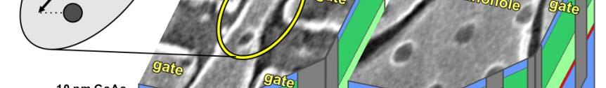
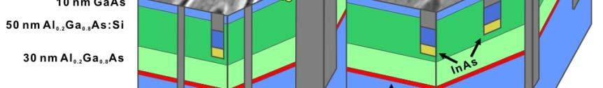
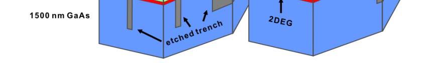
SUPPLEMENTARY FIGURES
 1 SUPPLEMENTARY FIGURES Supplementary Figure 1: Schematic representation of the experimental set up. The PC of the hot line being biased, the temperature raises. The temperature is extracted from noise
Nano-Electro-Mechanical Systems (NEMS) in the Quantum Limit
 in the Quantum Limit") Nano-Electro-Mechanical Systems (NEMS) in the Quantum Limit Eva Weig, now postdoc at University of California at Santa Barbara. Robert H. Blick, University of Wisconsin-Madison, Electrical & Computer Engineering,
Nano-Electro-Mechanical Systems (NEMS) in the Quantum Limit Eva Weig, now postdoc at University of California at Santa Barbara. Robert H. Blick, University of Wisconsin-Madison, Electrical & Computer Engineering,
Schottky diodes. JFETs - MESFETs - MODFETs
 Technische Universität Graz Institute of Solid State Physics Schottky diodes JFETs - MESFETs - MODFETs Quasi Fermi level When the charge carriers are not in equilibrium the Fermi energy can be different
Spin Filtering: how to write and read quantum information on mobile qubits
 Spin Filtering: how to write and read quantum information on mobile qubits Amnon Aharony Physics Department and Ilse Katz Nano institute Ora Entin-Wohlman (BGU), Guy Cohen (BGU) Yasuhiro Tokura (NTT) Shingo
Supplementary Figure 1. Supplementary Figure 1 Characterization of another locally gated PN junction based on boron
 Supplementary Figure 1 Supplementary Figure 1 Characterization of another locally gated PN junction based on boron nitride and few-layer black phosphorus (device S1). (a) Optical micrograph of device S1.
Carbon based Nanoscale Electronics
 Carbon based Nanoscale Electronics 09 02 200802 2008 ME class Outline driving force for the carbon nanomaterial electronic properties of fullerene exploration of electronic carbon nanotube gold rush of
For the following statements, mark ( ) for true statement and (X) for wrong statement and correct it.
 for true statement and (X) for wrong statement and correct it.") Benha University Faculty of Engineering Shoubra Electrical Engineering Department First Year communications. Answer all the following questions Illustrate your answers with sketches when necessary. The
Benha University Faculty of Engineering Shoubra Electrical Engineering Department First Year communications. Answer all the following questions Illustrate your answers with sketches when necessary. The
From nanophysics research labs to cell phones. Dr. András Halbritter Department of Physics associate professor
 From nanophysics research labs to cell phones Dr. András Halbritter Department of Physics associate professor Curriculum Vitae Birth: 1976. High-school graduation: 1994. Master degree: 1999. PhD: 2003.
Application II: The Ballistic Field-E ect Transistor
 Chapter 1 Application II: The Ballistic Field-E ect Transistor 1.1 Introduction In this chapter, we apply the formalism we have developed for charge currents to understand the output characteristics of
Physics of Semiconductors (Problems for report)
") Physics of Semiconductors (Problems for report) Shingo Katsumoto Institute for Solid State Physics, University of Tokyo July, 0 Choose two from the following eight problems and solve them. I. Fundamentals
Physics of Semiconductors (Problems for report) Shingo Katsumoto Institute for Solid State Physics, University of Tokyo July, 0 Choose two from the following eight problems and solve them. I. Fundamentals
Developing Quantum Logic Gates: Spin-Resonance-Transistors
 Developing Quantum Logic Gates: Spin-Resonance-Transistors H. W. Jiang (UCLA) SRT: a Field Effect Transistor in which the channel resistance monitors electron spin resonance, and the resonance frequency
ECE Branch GATE Paper The order of the differential equation + + = is (A) 1 (B) 2
 1 (B) 2") Question 1 Question 20 carry one mark each. 1. The order of the differential equation + + = is (A) 1 (B) 2 (C) 3 (D) 4 2. The Fourier series of a real periodic function has only P. Cosine terms if it is
Question 1 Question 20 carry one mark each. 1. The order of the differential equation + + = is (A) 1 (B) 2 (C) 3 (D) 4 2. The Fourier series of a real periodic function has only P. Cosine terms if it is
Graphene and Carbon Nanotubes
 Graphene and Carbon Nanotubes 1 atom thick films of graphite atomic chicken wire Novoselov et al - Science 306, 666 (004) 100μm Geim s group at Manchester Novoselov et al - Nature 438, 197 (005) Kim-Stormer
Classification of Solids
 Classification of Solids Classification by conductivity, which is related to the band structure: (Filled bands are shown dark; D(E) = Density of states) Class Electron Density Density of States D(E) Examples
Session 6: Solid State Physics. Diode
 Session 6: Solid State Physics Diode 1 Outline A B C D E F G H I J 2 Definitions / Assumptions Homojunction: the junction is between two regions of the same material Heterojunction: the junction is between
Martes Cuánticos. Quantum Capacitors. (Quantum RC-circuits) Victor A. Gopar
 Victor A. Gopar") Martes Cuánticos Quantum Capacitors (Quantum RC-circuits) Victor A. Gopar -Universal resistances of the quantum resistance-capacitance circuit. Nature Physics, 6, 697, 2010. C. Mora y K. Le Hur -Violation
Martes Cuánticos Quantum Capacitors (Quantum RC-circuits) Victor A. Gopar -Universal resistances of the quantum resistance-capacitance circuit. Nature Physics, 6, 697, 2010. C. Mora y K. Le Hur -Violation
Single Photon detectors
 Single Photon detectors Outline Motivation for single photon detection Semiconductor; general knowledge and important background Photon detectors: internal and external photoeffect Properties of semiconductor
Avalanche breakdown. Impact ionization causes an avalanche of current. Occurs at low doping
 Avalanche breakdown Impact ionization causes an avalanche of current Occurs at low doping Zener tunneling Electrons tunnel from valence band to conduction band Occurs at high doping Tunneling wave decays
Nanoscience, MCC026 2nd quarter, fall Quantum Transport, Lecture 1/2. Tomas Löfwander Applied Quantum Physics Lab
 Nanoscience, MCC026 2nd quarter, fall 2012 Quantum Transport, Lecture 1/2 Tomas Löfwander Applied Quantum Physics Lab Quantum Transport Nanoscience: Quantum transport: control and making of useful things
Room-Temperature Ballistic Nanodevices
 Encyclopedia of Nanoscience and Nanotechnology www.aspbs.com/enn Room-Temperature Ballistic Nanodevices Aimin M. Song Department of Electrical Engineering and Electronics, University of Manchester Institute
GaAs and InGaAs Single Electron Hex. Title. Author(s) Kasai, Seiya; Hasegawa, Hideki. Citation 13(2-4): Issue Date DOI
 Kasai, Seiya; Hasegawa, Hideki. Citation 13(2-4): Issue Date DOI") Title GaAs and InGaAs Single Electron Hex Circuits Based on Binary Decision D Author(s) Kasai, Seiya; Hasegawa, Hideki Citation Physica E: Low-dimensional Systems 3(2-4): 925-929 Issue Date 2002-03 DOI
Title GaAs and InGaAs Single Electron Hex Circuits Based on Binary Decision D Author(s) Kasai, Seiya; Hasegawa, Hideki Citation Physica E: Low-dimensional Systems 3(2-4): 925-929 Issue Date 2002-03 DOI
SPINTRONICS. Waltraud Buchenberg. Faculty of Physics Albert-Ludwigs-University Freiburg
 SPINTRONICS Waltraud Buchenberg Faculty of Physics Albert-Ludwigs-University Freiburg July 14, 2010 TABLE OF CONTENTS 1 WHAT IS SPINTRONICS? 2 MAGNETO-RESISTANCE STONER MODEL ANISOTROPIC MAGNETO-RESISTANCE
QUANTUM- CLASSICAL ANALOGIES
 D. Dragoman M. Dragoman QUANTUM- CLASSICAL ANALOGIES With 78 Figures ^Ü Springer 1 Introduction 1 2 Analogies Between Ballistic Electrons and Electromagnetic Waves 9 2.1 Analog Parameters for Ballistic
Zeeman splitting of single semiconductor impurities in resonant tunneling heterostructures
 Superlattices and Microstructures, Vol. 2, No. 4, 1996 Zeeman splitting of single semiconductor impurities in resonant tunneling heterostructures M. R. Deshpande, J. W. Sleight, M. A. Reed, R. G. Wheeler
Scanning gate microscopy and individual control of edge-state transmission through a quantum point contact
 Scanning gate microscopy and individual control of edge-state transmission through a quantum point contact Stefan Heun NEST, CNR-INFM and Scuola Normale Superiore, Pisa, Italy Coworkers NEST, Pisa, Italy:
Conventional Paper I (a) (i) What are ferroelectric materials? What advantages do they have over conventional dielectric materials?
 (i) What are ferroelectric materials? What advantages do they have over conventional dielectric materials?") Conventional Paper I-03.(a) (i) What are ferroelectric materials? What advantages do they have over conventional dielectric materials? (ii) Give one example each of a dielectric and a ferroelectric material
Conventional Paper I-03.(a) (i) What are ferroelectric materials? What advantages do they have over conventional dielectric materials? (ii) Give one example each of a dielectric and a ferroelectric material
Spin-orbit Effects in Semiconductor Spintronics. Laurens Molenkamp Physikalisches Institut (EP3) University of Würzburg
 University of Würzburg") Spin-orbit Effects in Semiconductor Spintronics Laurens Molenkamp Physikalisches Institut (EP3) University of Würzburg Collaborators Hartmut Buhmann, Charlie Becker, Volker Daumer, Yongshen Gui Matthias
Spin-orbit Effects in Semiconductor Spintronics Laurens Molenkamp Physikalisches Institut (EP3) University of Würzburg Collaborators Hartmut Buhmann, Charlie Becker, Volker Daumer, Yongshen Gui Matthias
Charging and Kondo Effects in an Antidot in the Quantum Hall Regime
 Semiconductor Physics Group Cavendish Laboratory University of Cambridge Charging and Kondo Effects in an Antidot in the Quantum Hall Regime M. Kataoka C. J. B. Ford M. Y. Simmons D. A. Ritchie University
8. Schottky contacts / JFETs
 Technische Universität Graz Institute of Solid State Physics 8. Schottky contacts / JFETs Nov. 21, 2018 Technische Universität Graz Institute of Solid State Physics metal - semiconductor contacts Photoelectric
Junction Diodes. Tim Sumner, Imperial College, Rm: 1009, x /18/2006
 Junction Diodes Most elementary solid state junction electronic devices. They conduct in one direction (almost correct). Useful when one converts from AC to DC (rectifier). But today diodes have a wide
File name: Supplementary Information Description: Supplementary Figures and Supplementary References. File name: Peer Review File Description:
 File name: Supplementary Information Description: Supplementary Figures and Supplementary References File name: Peer Review File Description: Supplementary Figure Electron micrographs and ballistic transport
Impact of disorder and topology in two dimensional systems at low carrier densities
 Impact of disorder and topology in two dimensional systems at low carrier densities A Thesis Submitted For the Degree of Doctor of Philosophy in the Faculty of Science by Mohammed Ali Aamir Department
An RF Circuit Model for Carbon Nanotubes
 IEEE TRANSACTIONS ON NANOTECHNOLOGY, VOL. 2, NO. 1, MARCH 2003 55 An RF Circuit Model for Carbon Nanotubes Abstract We develop an RF circuit model for single walled carbon nanotubes for both dc and capacitively
Optical Nonlinearities in Quantum Wells
 Harald Schneider Institute of Ion-Beam Physics and Materials Research Semiconductor Spectroscopy Division Rosencher s Optoelectronic Day Onéra 4.05.011 Optical Nonlinearities in Quantum Wells Harald Schneider
Chapter 5. Semiconductor Laser
 Chapter 5 Semiconductor Laser 5.0 Introduction Laser is an acronym for light amplification by stimulated emission of radiation. Albert Einstein in 1917 showed that the process of stimulated emission must
9. Semiconductor Devices /Phonons
 Technische Universität Graz Institute of Solid State Physics 9. Semiconductor Devices /Phonons Oct 29, 2018 p and n profiles p n V bi ~ 1 V E c W ~ 1 m E F E max ~ 10 4 V/cm ev bi E v p Ev E F Nv exp kt
Semiconductors and Optoelectronics. Today Semiconductors Acoustics. Tomorrow Come to CH325 Exercises Tours
 Semiconductors and Optoelectronics Advanced Physics Lab, PHYS 3600 Don Heiman, Northeastern University, 2017 Today Semiconductors Acoustics Tomorrow Come to CH325 Exercises Tours Semiconductors and Optoelectronics
SUPPLEMENTARY INFORMATION
 SUPPLEMENTARY INFORMATION DOI: 10.1038/NNANO.2011.138 Graphene Nanoribbons with Smooth Edges as Quantum Wires Xinran Wang, Yijian Ouyang, Liying Jiao, Hailiang Wang, Liming Xie, Justin Wu, Jing Guo, and
Physics of Low-Dimensional Semiconductor Structures
 Physics of Low-Dimensional Semiconductor Structures Edited by Paul Butcher University of Warwick Coventry, England Norman H. March University of Oxford Oxford, England and Mario P. Tosi Scuola Normale
Lecture 2. Introduction to semiconductors Structures and characteristics in semiconductors
 Lecture 2 Introduction to semiconductors Structures and characteristics in semiconductors Semiconductor p-n junction Metal Oxide Silicon structure Semiconductor contact Literature Glen F. Knoll, Radiation
Spring Semester 2012 Final Exam
 Spring Semester 2012 Final Exam Note: Show your work, underline results, and always show units. Official exam time: 2.0 hours; an extension of at least 1.0 hour will be granted to anyone. Materials parameters
Preview from Notesale.co.uk Page 4 of 35
 field 64 If a dielectric is inserted b/w the plates of a charged capacitor, its Remains Becomes infinite capacitance constant decreases increases 65 Selenium is an insulator in the dark but when exposed
Semiconductor Quantum Structures And Energy Conversion. Itaru Kamiya Toyota Technological Institute
 Semiconductor Quantum Structures And nergy Conversion April 011, TTI&NCHU Graduate, Special Lectures Itaru Kamiya kamiya@toyota-ti.ac.jp Toyota Technological Institute Outline 1. Introduction. Principle
Enhancement-mode quantum transistors for single electron spin
 Purdue University Purdue e-pubs Other Nanotechnology Publications Birck Nanotechnology Center 8-1-2006 Enhancement-mode quantum transistors for single electron spin G. M. Jones B. H. Hu C. H. Yang M. J.
Quantum-dot cellular automata
 Quantum-dot cellular automata G. L. Snider, a) A. O. Orlov, I. Amlani, X. Zuo, G. H. Bernstein, C. S. Lent, J. L. Merz, and W. Porod Department of Electrical Engineering, University of Notre Dame, Notre
Project Periodic Report
 Project Periodic Report Publishable Summary Grant Agreement n. 256959 Project title Nanoscale energy management for powering ICT devices Project acronym NANOPOWER Call identifier FP7-ICT-2009-5 Funding
Quantum Interference and Decoherence in Hexagonal Antidot Lattices
 Quantum Interference and Decoherence in Hexagonal Antidot Lattices Yasuhiro Iye, Masaaki Ueki, Akira Endo and Shingo Katsumoto Institute for Solid State Physics, University of Tokyo, -1- Kashiwanoha, Kashiwa,
Universal valence-band picture of. the ferromagnetic semiconductor GaMnAs
 Universal valence-band picture of the ferromagnetic semiconductor GaMnAs Shinobu Ohya *, Kenta Takata, and Masaaki Tanaka Department of Electrical Engineering and Information Systems, The University of
Demonstration of a functional quantum-dot cellular automata cell
 Demonstration of a functional quantum-dot cellular automata cell Islamshah Amlani, a) Alexei O. Orlov, Gregory L. Snider, Craig S. Lent, and Gary H. Bernstein Department of Electrical Engineering, University
Operation and Modeling of. The MOS Transistor. Second Edition. Yannis Tsividis Columbia University. New York Oxford OXFORD UNIVERSITY PRESS
 Operation and Modeling of The MOS Transistor Second Edition Yannis Tsividis Columbia University New York Oxford OXFORD UNIVERSITY PRESS CONTENTS Chapter 1 l.l 1.2 1.3 1.4 1.5 1.6 1.7 Chapter 2 2.1 2.2
OPTI510R: Photonics. Khanh Kieu College of Optical Sciences, University of Arizona Meinel building R.626
 OPTI510R: Photonics Khanh Kieu College of Optical Sciences, University of Arizona kkieu@optics.arizona.edu Meinel building R.626 Announcements HW#3 is assigned due Feb. 20 st Mid-term exam Feb 27, 2PM
Final Examination EE 130 December 16, 1997 Time allotted: 180 minutes
 Final Examination EE 130 December 16, 1997 Time allotted: 180 minutes Problem 1: Semiconductor Fundamentals [30 points] A uniformly doped silicon sample of length 100µm and cross-sectional area 100µm 2
Formation of unintentional dots in small Si nanostructures
 Superlattices and Microstructures, Vol. 28, No. 5/6, 2000 doi:10.1006/spmi.2000.0942 Available online at http://www.idealibrary.com on Formation of unintentional dots in small Si nanostructures L. P. ROKHINSON,
Solid State Device Fundamentals
 Solid State Device Fundamentals ENS 345 Lecture Course by Alexander M. Zaitsev alexander.zaitsev@csi.cuny.edu Tel: 718 982 2812 Office 4N101b 1 Outline - Goals of the course. What is electronic device?
Correlated 2D Electron Aspects of the Quantum Hall Effect
 Correlated 2D Electron Aspects of the Quantum Hall Effect Magnetic field spectrum of the correlated 2D electron system: Electron interactions lead to a range of manifestations 10? = 4? = 2 Resistance (arb.
Impact of Silicon Wafer Orientation on the Performance of Metal Source/Drain MOSFET in Nanoscale Regime: a Numerical Study
 JNS 2 (2013) 477-483 Impact of Silicon Wafer Orientation on the Performance of Metal Source/Drain MOSFET in Nanoscale Regime: a Numerical Study Z. Ahangari *a, M. Fathipour b a Department of Electrical
Coulomb blockade in metallic islands and quantum dots
 Coulomb blockade in metallic islands and quantum dots Charging energy and chemical potential of a metallic island Coulomb blockade and single-electron transistors Quantum dots and the constant interaction
ECE 546 Lecture 10 MOS Transistors
 ECE 546 Lecture 10 MOS Transistors Spring 2018 Jose E. Schutt-Aine Electrical & Computer Engineering University of Illinois jesa@illinois.edu NMOS Transistor NMOS Transistor N-Channel MOSFET Built on p-type
Review of Semiconductor Physics. Lecture 3 4 Dr. Tayab Din Memon
 Review of Semiconductor Physics Lecture 3 4 Dr. Tayab Din Memon 1 Electronic Materials The goal of electronic materials is to generate and control the flow of an electrical current. Electronic materials
Charge spectrometry with a strongly coupled superconducting single-electron transistor
 PHYSICAL REVIEW B, VOLUME 64, 245116 Charge spectrometry with a strongly coupled superconducting single-electron transistor C. P. Heij, P. Hadley, and J. E. Mooij Applied Physics and Delft Institute of
Solar Cell Materials and Device Characterization
 Solar Cell Materials and Device Characterization April 3, 2012 The University of Toledo, Department of Physics and Astronomy SSARE, PVIC Principles and Varieties of Solar Energy (PHYS 4400) and Fundamentals
Physics and Material Science of Semiconductor Nanostructures
 Physics and Material Science of Semiconductor Nanostructures PHYS 570P Prof. Oana Malis Email: omalis@purdue.edu Course website: http://www.physics.purdue.edu/academic_programs/courses/phys570p/ 1 Course
Photonic Crystal Nanocavities for Efficient Light Confinement and Emission
 Journal of the Korean Physical Society, Vol. 42, No., February 2003, pp. 768 773 Photonic Crystal Nanocavities for Efficient Light Confinement and Emission Axel Scherer, T. Yoshie, M. Lončar, J. Vučković
CME 300 Properties of Materials. ANSWERS: Homework 9 November 26, As atoms approach each other in the solid state the quantized energy states:
 CME 300 Properties of Materials ANSWERS: Homework 9 November 26, 2011 As atoms approach each other in the solid state the quantized energy states: are split. This splitting is associated with the wave
Laurens W. Molenkamp. Physikalisches Institut, EP3 Universität Würzburg
 Laurens W. Molenkamp Physikalisches Institut, EP3 Universität Würzburg Onsager Coefficients I electric current density J particle current density J Q heat flux, heat current density µ chemical potential
Index. buried oxide 35, 44 51, 89, 238 buried channel 56
 Index A acceptor 275 accumulation layer 35, 45, 57 activation energy 157 Auger electron spectroscopy (AES) 90 anode 44, 46, 55 9, 64, 182 anode current 45, 49, 65, 77, 106, 128 anode voltage 45, 52, 65,
Anisotropic spin splitting in InGaAs wire structures
 Available online at www.sciencedirect.com Physics Physics Procedia Procedia 3 (010) 00 (009) 155 159 000 000 14 th International Conference on Narrow Gap Semiconductors and Systems Anisotropic spin splitting
Construction of a reconfigurable dynamic logic cell
 PRAMANA c Indian Academy of Sciences Vol. 64, No. 3 journal of March 2005 physics pp. 433 441 Construction of a reconfigurable dynamic logic cell K MURALI 1, SUDESHNA SINHA 2 and WILLIAM L DITTO 3 1 Department
Graphene photodetectors with ultra-broadband and high responsivity at room temperature
 SUPPLEMENTARY INFORMATION DOI: 10.1038/NNANO.2014.31 Graphene photodetectors with ultra-broadband and high responsivity at room temperature Chang-Hua Liu 1, You-Chia Chang 2, Ted Norris 1.2* and Zhaohui
Quantum Size Effect of Two Couple Quantum Dots
 EJTP 5, No. 19 2008) 33 42 Electronic Journal of Theoretical Physics Quantum Size Effect of Two Couple Quantum Dots Gihan H. Zaki 1), Adel H. Phillips 2) and Ayman S. Atallah 3) 1) Faculty of Science,
Quantum Confinement in Graphene
 Quantum Confinement in Graphene from quasi-localization to chaotic billards MMM dominikus kölbl 13.10.08 1 / 27 Outline some facts about graphene quasibound states in graphene numerical calculation of
Lecture 18: Semiconductors - continued (Kittel Ch. 8)
") Lecture 18: Semiconductors - continued (Kittel Ch. 8) + a - Donors and acceptors J U,e e J q,e Transport of charge and energy h E J q,e J U,h Physics 460 F 2006 Lect 18 1 Outline More on concentrations
Lecture 18: Semiconductors - continued (Kittel Ch. 8) + a - Donors and acceptors J U,e e J q,e Transport of charge and energy h E J q,e J U,h Physics 460 F 2006 Lect 18 1 Outline More on concentrations
Principles and Applications of Superconducting Quantum Interference Devices (SQUIDs)
") Principles and Applications of Superconducting Quantum Interference Devices (SQUIDs) PHY 300 - Junior Phyics Laboratory Syed Ali Raza Roll no: 2012-10-0124 LUMS School of Science and Engineering Thursday,
Principles and Applications of Superconducting Quantum Interference Devices (SQUIDs) PHY 300 - Junior Phyics Laboratory Syed Ali Raza Roll no: 2012-10-0124 LUMS School of Science and Engineering Thursday,