Tackling the Little Box Challenge - New circuit architectures to achieve a 216 W/in 3 power density 2 kw inverter
|
|
|
- Basil Blankenship
- 6 years ago
- Views:
Transcription
1 Tackling the Little Box Challenge - New circuit architectures to achieve a 6 W/in 3 power density kw inverter Robert Pilawa-Podgurski, Yutian Lei, Shibin Qin, Chris Barth, Wen-Chuen Liu, Andrew Stillwell, Intae Moon, Derek Chou, Thomas Foulkes, Zitao Liao, Zichao Ye Pilawa Research Group University of Illinois Urbana-Champaign IEEE PELS Webinar, May 5, 06
2 Outline Competition background Technical challenges Twice line frequency ripple compensation Conventional approaches Series-stacked buffer architecture Experimental measurements AC waveform generation Conventional approaches Flying-capacitor multi-level converter background Integrated switching cell development Experimental results Performance evaluation and comparison Lessons learned and future research directions

, must run for 00 hours")
3 Google/IEEE Little Box Challenge kw, single-phase 40 V, 60 Hz AC Example usage: solar inverter, electric car charger, grid storage integration Current state-of-the-art: 95% efficiency, 400 in 3. Target goal: >95% efficiency, 0x smaller (40 in 3 ), must run for 00 hours $M prize to winning entry 3
4 To Participate or not Participate? Why not participate? We had no prior inverter experience Winning solution likely one that sacrifices reliability (e.g., 0 hour operation) Rules more suitable for industry -year timeline to develop inverter from scratch Rigorous testing protocol -> robustness required FCC Class B (including radiated!) Most people told us that Kolar s team at ETH will likely win anyway Why participate? Compete against the best teams in the world Students will learn valuable skills EMI, packaging, thermal, etc. A chance to compare our new research ideas against a common benchmark 4
5 Our Goal Develop a radically different solution make significant research contribution to the field of power electronics. May not win competition, but will have long-term impact 5


6 Original Team Chris Barth Integration Mechanical Thermal Capacitor evaluation Yutian Lei Inverter design Inverter control Shibin Qin Twice-linefrequency buffering System control $30k funding through Google Academic Grant 6

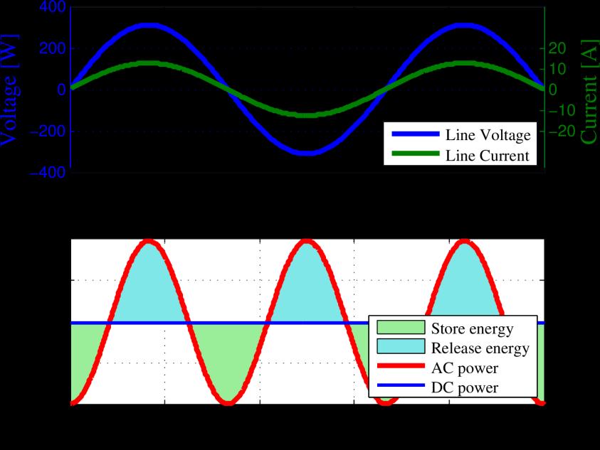
7 Key Technical Challenges E store = P dc πf line 7

8 Conventional Solution -Passive Filtering Capacitor as energy storage E store = P dc πf line = CV max CV min = C V max + V min V max V min nominal bus voltage bus voltage ripple 8
9 Active Filtering Ripple Port Converter π P ave Advantages Capacitor ripple decoupled from bus ripple Increased energy utilization of capacitor Smaller overall size Disadvantages High buffer converter power rating High voltage stress Low switching frequency, large inductor(s) Overall efficiency reduced: η buf = η dc-ac = 95% η total = 9.4% Krein et al., Minimum energy and capacitor requirement for single-phase inverters and rectifiers using a ripple port, IEEE TPELS, Nov, 0 Hu et al., A single-stage micro-inverter without using electrolytic capacitors, IEEE TPELS, June, 03 9
10 Stacked Switched-Capacitor Buffer Advantages No inductor Potentially higher efficiency (slow switching action) Reduced switch rating possible Disadvantages Large bus ripple Lower energy utilization of capacitors Increased circuit complexity Gate drivers, etc. Chen et al, "Stacked Switched Capacitor Energy Buffer Architecture," TPELS 03 0
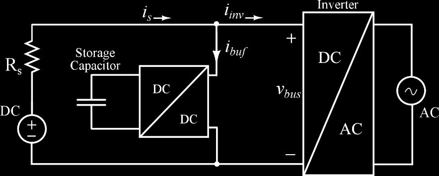

11 Series-Stacked Buffer Architecture Series-Stacked Buffer
12 Series-Stacked Buffer Converter A series-connected buffer converter Reduced voltage stress (C blocks majority of voltage) Enable low voltage transistors - > Buffer converter size reduction Partial power processing (extreme efficiencies possible) Low power rating of buffer converter Size reduction Qin et al., A High-Efficiency High Energy Density Buffer Architecture for Power Pulsation Decoupling in Grid-Interfaced Converters, ECCE 05
 of overall power -> greatly improved efficiency")
13 Circuit Architecture - Overview i buf controlled to provide difference between i s and i inv v c + v ab constant Buffer converter processes fraction (7% here) of overall power -> greatly improved efficiency 3
14 Control Challenge: Voltage Balancing Buffer converter introduces loss C will slowly discharge, unless compensated Must provide additional charge to C Can recharge C through external means - undesirable 4
 i buf pure AC, v C pure AC v bus DC + small AC")

15 Control Challenge: Voltage Balancing Load step Enable compensation Buffer converter power =i buf v ab = i buf (v bus v C ) i buf pure AC, v C pure AC v bus DC + small AC (ripple) Qin et al., Architecture and control of an high energy density buffer for power pulsation decoupling in grid-interfaced applications, COMPEL 05 [Best paper award] 5


16 Hardware Implementation Capacitor Choices Metal film Very low loss Constant capacitance Low energy density Ceramic Low loss Capacitance reduced with applied voltage High energy density Electrolytic High loss High constant capacitance RMS current limited Poor reliablity 6


17 Experimental Verification of Energy Storage Experimental test setup is configured to measure energy storage over wide voltage swing. Voltage swing and bias are independently adjustable. Capacitor test fixture 7


18 Experimental Results Experimental waveforms: Film capacitor with constant capacitance Ceramic capacitor with varying capacitance 8
19 Experimental Results Measured energy density for a range of capacitors and voltage ratings. RMS current limited C. Barth, I. Moon, Y. Lei, S. Qin and R.C.N. Pilawa-Podgurski Experimental Evaluation of Capacitors for Power Buffering in Single-Phase Power Converters, IEEE Energy Conversion Congress and Exposition, Montreal, Canada, 05 9
20 Experimental Results Quality factor normalizes energy stored by loss. 0
21 Experimental Results Film (PP), 300V, 60uF X7T, 450 V,. uf X6S, 450V,. uf C. Barth, I. Moon, Y. Lei, S. Qin and R.C.N. Pilawa-Podgurski Experimental Evaluation of Capacitors for Power Buffering in Single-Phase Power Converters, IEEE Energy Conversion Congress and Exposition, Montreal, Canada, 05
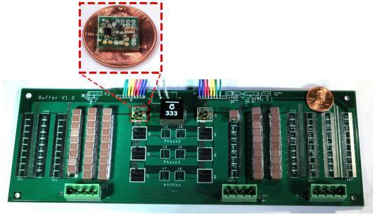
22 Hardware Prototypes TI LMG W/inch^3 ~80 W/inch^3
 - 400 V ~ 450V bus voltage, - 0 A peak to peak current 98.")

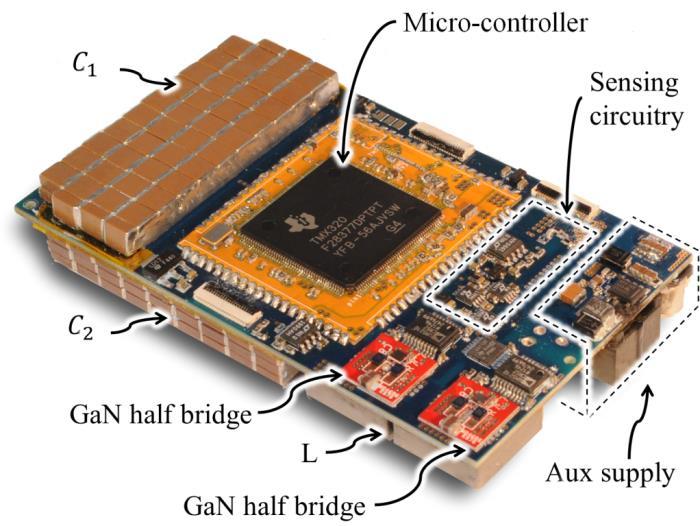
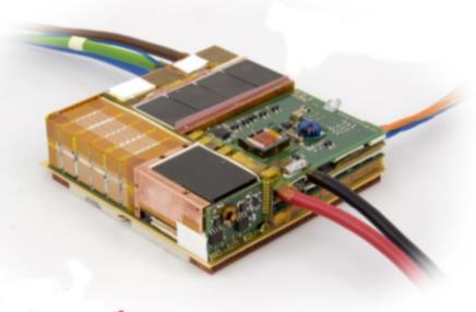
23 Hardware Prototype Energy Density Design requirement: - kva (PF = 0.7~) V ~ 450V bus voltage, - 0 A peak to peak current 98.0mm auxiliary supply Way of measurement Volume Power density 58.3mm sensing circuitry Rectangular box 4.88 inch^3 40 W/inch^3 4.0mm C microcontroller GaN full bridge passive component.0 inch^3 995 W/inch^3 C inductor 99% efficiency across load range C C 3 C bus auxiliary supply 3


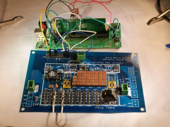
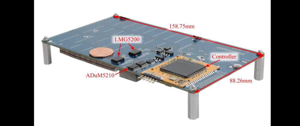
24 Final Hardware Prototype Isolator ADuM50 Current sensing: LT999 Voltage sensing: LT990 EPC 06C / LMG V switch TDK X6S capacitors TI Delfino F8377D 4

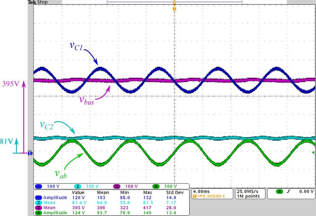
25 Experiment - Steady State Operation 5


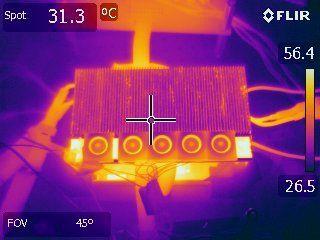
26 Experiment - Transient Operation 5% load to 50% load 00% load to 75% load 6

27 Experiment - Efficiency Digital power meter, integral function to ensure accuracy Same setup that was used to characterize capacitors Efficiency measurement excludes about 3 W control and gate driving power 7
28 Key Technical Challenges E store = P dc πf line 8
")

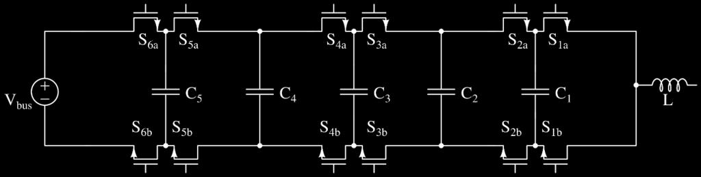
29 Inverter Conventional Topology Conventional Inverter H-bridge (likely dual interleaved) 650 V GaN transistors High switch stress High dv/dt Large inductor Localized hot spots 9
 Heat spreading Inductor reduced by (N ) T. Meynard and H.")
30 Multi-Level Flying-Capacitor Converter Inductor ripple frequency: f sw (N ) Reduced ripple voltage amplitude: V DC (N ) Reduced switch voltage stress: V DC (N ) Heat spreading Inductor reduced by (N ) T. Meynard and H. Foch, Multi-level conversion: high voltage choppers and voltage-source inverters, PESC 9 30
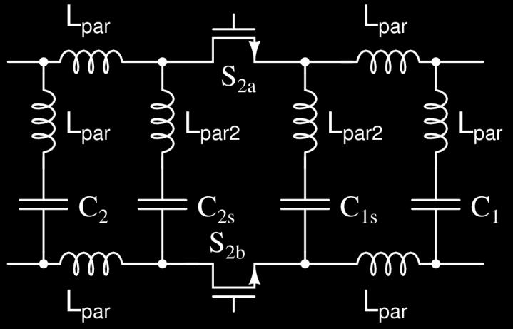
31 Multi-level Operation S 3a S a S a C C V sw V sw V in V in V in + V in V in
32 Multi-level Operation S 3a S a S a C C V sw V sw V in V in V in + V in V in
33 Multi-level Operation S 3a S a S a C C V sw V sw V in V in V in + V in V in
34 Multi-level Operation S 3a S a S a C C V sw V sw V in V in V in + V in V in
35 Multi-level Operation S 3a S a S a C C V sw V sw V in V in V in + V in V in
36 Multi-level Operation S 3a S a S a C C V sw V sw V in V in V in + V in V in
37 Multi-level Operation S 3a S a S a C C V sw V sw V in V in V in + V in V in
38 Multi-level Operation S 3a S a S a C C V sw V sw V in S 3a S a S a 3 V V in sw 0 0
39 Multi-level Operation S 3a S a S a C C V sw V sw V in S 3a S a S a 3 V V in sw 0 0 0
40 Multi-level Operation S 3a S a S a C C V sw V sw V in S 3a S a S a 3 V V in sw 0 0
41 Multi-level Operation S 3a S a S a C C V sw V sw V in S 3a S a S a 3 V V in sw 0 0 0
42 Multi-level Operation S 3a S a S a C C V sw V sw V in S 3a S a S a 3 V V in sw 0 0
43 Multi-level Operation S 3a S a S a C C V sw V sw V in S 3a S a S a 3 V V in sw 0 0 0

44 Multi-level Operation S 3a S a S a C C V sw V sw V in S 3a S a pulse in each period S a 3 V V in sw 3 pulses in each switching period
, 450 V -> 75 V Alternates")
 Reduction")

45 Our Proposed DC-AC Conversion Stage Advantages Low voltage switch: V DC /(N-), 450 V -> 75 V Alternates capacitor charging and discharging at switching frequency (compare to line frequency of MMC) Reduction in output filter size T. Meynard and H. Foch, Multi-level conversion: high voltage choppers and voltage-source inverters, PESC 9 45
46 Implementation Challenges Few experimentally demonstrated examples of > 5 level flying capacitor multi-level inverter, and none switching in the 00 s of khz at kw levels. Challenges Capacitor voltage balancing Approach: natural balancing with phase-shifted PWM Gate driving complexity Approach: Half-bridge gate drivers (LM53) and integrated isolated dcdc converter (ADUM50) Parasitic inductance Fast turn-on needed to reduce the V-I overlap loss during switching High dv/dt causes V ds ringing 46

47 Implementation Challenges 47

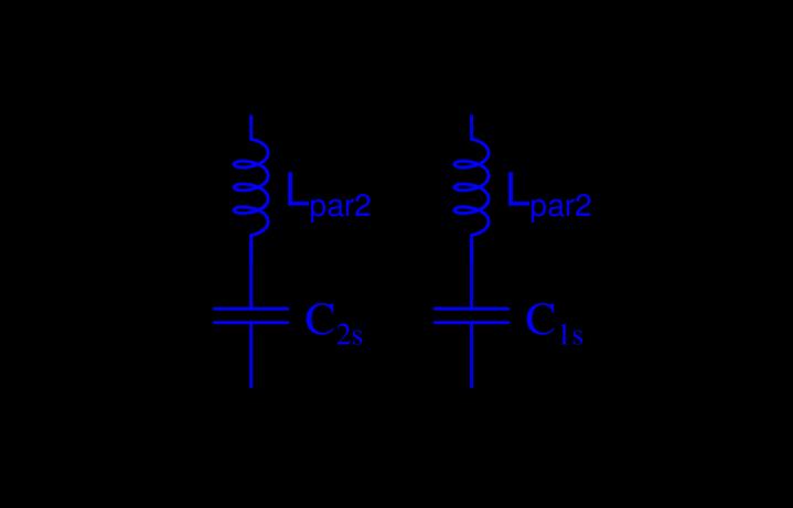
48 Parasitic Loop Inductance 48


49 Integrated Switching Cell 49

50 Digital Control Control objective: Generate correct amplitude Switch only minimum inductance loops Maintain capacitor voltage balance 50

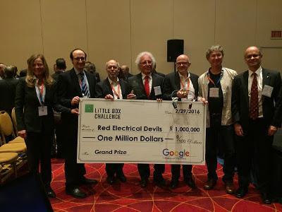
51 Prototype # 80 W/in 3, 98% efficient 000+ total entries July 3, 05, 00+ submitted final report 8 finalists selected to October, 05 NREL testing 5
52 Growing the Team 5


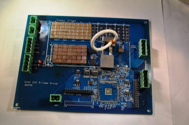
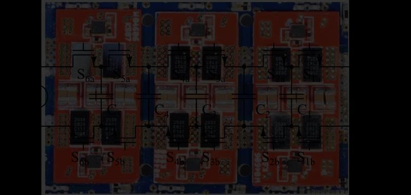
53 Shrinking the Hardware 53

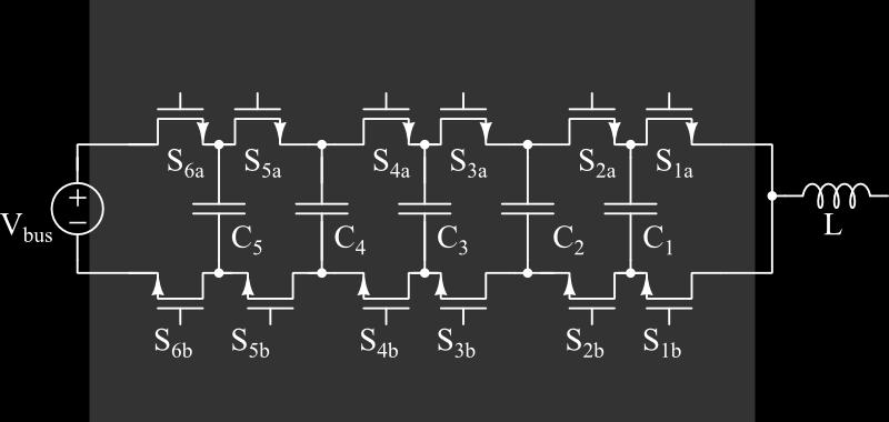
54 kw Hardware Prototype Y. Lei, C. Barth, S. Qin, W.-C. Liu, I. Moon, A. Stillwell, D. Chou, T. Foulkes, Z. Ye, Z. Liao and R.C.N. Pilawa-Podgurski A kw, Single-Phase, 7-Level, GaN Inverter with an Active Energy Buffer Achieving 6 W/in^3 Power Density and 97.6% Peak Efficiency, IEEE Applied Power Electronics Conference, Long Beach, CA, 06 54
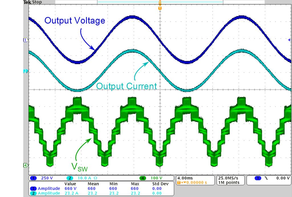
55 Experimental Results 0.3% THD 55

56 Resulting Performance 97.6% efficiency 6 W/in^3 Commercial off-the-shelf components No electrolytic buffer capacitors All student-team $30k budget (not including night and weekend work!) Innovation in both inverter and buffer converter Our nd iteration Plenty of room for improvements EMI filtering inductors 56
 Drop-off inverters for extensive testing")
 00 hour continuous operation")
57 NREL Testing October st, NREL Finalist symposium 8 teams invited (3 no-shows) Drop-off inverters for extensive testing Check all specifications Ripple, EMI, temperature, etc Load steps (extent unknown to teams) 00 hour continuous operation 57
58 Performance Comparison (Best Estimate) Excellent technical details/comparison by Prof. Johann Kolar at CIPS 06 Keynote: CIPS_6_Keynote_Presentation_FINAL_as_published_09036.pdf 58


59 Selected Teams (efficiencies at kw) 59


60 NREL Testing Details Difficult to exactly replicate testing scenarios 60
61 Research Impact Demonstrated the feasibility of multi-level flying capacitor power converters At kw-scale Using GaN technology With 70 khz effective switching frequency Achieved high efficiency and high power density through a new series-stacked active buffer Much work remains to be done for industry adoption Gate driver, isolated power supplies, level shifting Robustness, integration Approach likely to be relevant in applications where power density is a key requirement Laid the foundation for several promising future research areas 6
62 Lessons Learned Teams: Tempting to try to squeeze in too much innovation Timeline very challenging Great opportunity to learn from other teams Fantastic technical discussions Common bonding experience Reliability was overlooked by many teams Organizers: Difficult to set specs correctly the first time Many good teams left out from finalist selection Should consider allowing participants to test inverter at testing location IEEE: Significant value in having a common benchmark to compare approaches 6
63 Acknowledgments Google Texas Instruments NASA TDK Grainger CEME at UIUC 63

64 The Team Questions? 64
65 Backup Slides 65


66 Estimated Power Loss Breakdown 66
67 Full Specifications 67
THE power transfer capability is one of the most fundamental
 4172 IEEE TRANSACTIONS ON POWER ELECTRONICS, VOL. 27, NO. 9, SEPTEMBER 2012 Letters Power Characterization of Isolated Bidirectional Dual-Active-Bridge DC DC Converter With Dual-Phase-Shift Control Biao
Electrical and Thermal Packaging Challenges for GaN Devices. Paul L. Brohlin Texas Instruments Inc. October 3, 2016
 Electrical and Thermal Packaging Challenges for GaN Devices Paul L. Brohlin Texas Instruments Inc. October 3, 2016 1 Outline Why GaN? Hard-Switching Losses Parasitic Inductance Effects on Switching Thermal
Power electronics Slobodan Cuk
 Power electronics Slobodan Cuk came to Caltech in 1974 and obtained his PhD degree in Power Electronics in 1976. From 1977 until December, 1999 he was at the California Institute of Technology where he
Novel DC-AC Converter Topology for Multilevel Battery Energy Storage Systems. Mario Gommeringer, Felix Kammerer, Johannes Kolb, Michael Braun
 Elektrotechnisches Institut (ETI) Prof. Dr.-Ing. Michael Braun Prof. Dr.-Ing. Martin Doppelbauer Prof. Dr.-Ing. Marc Hiller Kaiserstr.12. 76131 Karlsruhe 13. Sept. 216 Title: Novel DC-C Converter Topology
LECTURE 8 Fundamental Models of Pulse-Width Modulated DC-DC Converters: f(d)
") 1 ECTURE 8 Fundamental Models of Pulse-Width Modulated DC-DC Converters: f(d) I. Quasi-Static Approximation A. inear Models/ Small Signals/ Quasistatic I V C dt Amp-Sec/Farad V I dt Volt-Sec/Henry 1. Switched
1 ECTURE 8 Fundamental Models of Pulse-Width Modulated DC-DC Converters: f(d) I. Quasi-Static Approximation A. inear Models/ Small Signals/ Quasistatic I V C dt Amp-Sec/Farad V I dt Volt-Sec/Henry 1. Switched
Distributing Tomorrow s Technologies For Today s Designs Toll-Free:
 2W, Ultra-High Isolation DIP, Single & DC/DC s Key Features Low Cost 6 Isolation MTBF > 6, Hours Short Circuit Protection Input, and 24 Output,, 1, {, { and {1 Regulated Outputs Low Isolation Capacitance
ET4119 Electronic Power Conversion 2011/2012 Solutions 27 January 2012
 ET4119 Electronic Power Conversion 2011/2012 Solutions 27 January 2012 1. In the single-phase rectifier shown below in Fig 1a., s = 1mH and I d = 10A. The input voltage v s has the pulse waveform shown
 Distributed by: www.jameco.com 1-800-831-4242 The content and copyrights of the attached material are the property of its owner. DS0026 Dual High-Speed MOS Driver General Description DS0026 is a low cost
Design and Control of a Buck Boost Charger-Discharger for DC-Bus Regulation in Microgrids
 energies Article Design and Control of a Buck Boost Charger-Discharger for DC-Bus Regulation in Microgrids Carlos Andrés Ramos-Paja 1, *, ID, Juan David Bastidas-Rodríguez 2 ID, Daniel González 3 ID, Santiago
MAU100 Series. 1W, Miniature SIP, Single & Dual Output DC/DC Converters MINMAX. Key Features
 W, Miniature SIP, Single & Dual Output DC/DC s Key Features Efficiency up to % 000 Isolation MTBF >,000,000 Hours Low Cost Input,, and Output 3.3,,9,,,{,{9,{ and { Temperature Performance -0] to +] UL
R. W. Erickson. Department of Electrical, Computer, and Energy Engineering University of Colorado, Boulder
 . W. Erickson Department of Electrical, Computer, and Energy Engineering University of Colorado, Boulder Part II" Converter Dynamics and Control! 7.!AC equivalent circuit modeling! 8.!Converter transfer
Power Density Optimization of Resonant Tanks Using Standard Capacitors
 Power Density Optimization of Resonant Tanks Using Standard Capacitors Phyo Aung Kyaw, Aaron L.F. Stein, Charles R. Sullivan Thayer School of Engineering at Dartmouth Hanover, NH 03755, USA {phyo.a.kyaw.th,
ECE1750, Spring Week 11 Power Electronics
 ECE1750, Spring 2017 Week 11 Power Electronics Control 1 Power Electronic Circuits Control In most power electronic applications we need to control some variable, such as the put voltage of a dc-dc converter,
The output voltage is given by,
 71 The output voltage is given by, = (3.1) The inductor and capacitor values of the Boost converter are derived by having the same assumption as that of the Buck converter. Now the critical value of the
Application Note. Paralleling of EconoPACK TM + Date: Page
 Date: 27.09.2004 Page 1 Paralleling of EconoPACK TM + 1. EconoPACK TM + Design 2. Paralleling of IGBT 3 and EmCon HE diodes 3. Methods of paralleling EconoPACK TM + 4. Dynamic and static current sharing
MAU100 Series. 1W, Miniature SIP, Single & Dual Output DC/DC Converters MINMAX. Block Diagram. Key Features
 MAU Series W, Miniature SIP, Single & DC/DC s Key Features Efficiency up to 0 Isolation MTBF >,000,000 Hours Low Cost Input,, and Output 3.3,,9,,,{,{9,{ and { Temperature Performance -0 to UL 9V-0 Package
Requirements for Circuit Components of Single-Phase Inverter Applied with Power Decoupling Capability toward High Power Density
 Requirements for Circuit Components of Single-Phase Inverter Applied with Power Decoupling Capability toward High Power Density Keywords Jun-ichi Itoh, Tomokazu Sakuraba, Hoai Nam Le, Keisuke Kusaka Nagaoka
Implementation Possibilities of SMD Capacitors for High Power Applications
 doi: 10.2478/v10314-012-0003-2 2012 / 1 Implementation Possibilities of MD Capacitors for High Power Applications Janis Zakis (enior Research Fellow, Tallinn University of Technology), Dmitri Vinnikov
Regulated DC-DC Converter
 Regulated DC-DC Converter Zabir Ahmed Lecturer, BUET Jewel Mohajan Lecturer, BUET M A Awal Graduate Research Assistant NSF FREEDM Systems Center NC State University Former Lecturer, BUET 1 Problem Statement
Hybrid Predictive and Input-output feedback linearization controllers design for Half Bridge Multicellular Inverter: Comparative study
 The nd International Conference on Power Electronics and their Applications (ICPEA 5), Djelfa on 9-3 March 5, Algeria Hybrid Predictive and Input-output feedback linearization controllers design for Half
Benefits of Stacked-Wafer Capacitors for High-Frequency Buck Converters
 Benefits of Stacked-Wafer Capacitors for High-Frequency Buck Converters Michael W. Baker, PhD Maxim Integrated Power SoC Northeastern University, Boston MA. October 7, 2014 Mobile Device Trends Power Management
MAU200 Series. 1W, High Isolation SIP, Single & Dual Output DC/DC Converters MINMAX. Block Diagram. Key Features
 Component Distributors, Inc. ~ www.cdiweb.com ~ sales@cdiweb.com ~ -0--33 W, High Isolation SIP, Single & DC/DC s Key Features Efficiency up to 00 Isolation MTBF >,000,000 Hours Low Cost Input, and Output
Chapt ha e pt r e r 9 Capacitors
 Chapter 9 Capacitors Basics of a Capacitor In its simplest form, a capacitor is an electrical device constructed of two parallel plates separated by an insulating material called the dielectric In the
Switched Capacitor Circuits I. Prof. Paul Hasler Georgia Institute of Technology
 Switched Capacitor Circuits I Prof. Paul Hasler Georgia Institute of Technology Switched Capacitor Circuits Making a resistor using a capacitor and switches; therefore resistance is set by a digital clock
Designing an LLC Resonant Half-Bridge Power Converter
 Topic 3 Designing an LLC Resonant Half-Bridge Power Converter Hong Huang Agenda. Introduction Brief review Advantages 2. Design Prerequisites Configuration Operation Modeling Voltage gain function 3. Design
Power Electronics
 Prof. Dr. Ing. Joachim Böcker Power Electronics 3.09.06 Last Name: Student Number: First Name: Study Program: Professional Examination Performance Proof Task: (Credits) (0) (0) 3 (0) 4 (0) Total (80) Mark
DISTURBANCE LOAD MODELLING WITH EQUIVALENT VOLTAGE SOURCE METHOD IN GRID HARMONIC ASSESSMENT
 DISTURBANCE LOAD MODELLING WITH EQUIVALENT VOLTAGE SOURCE METHOD IN GRID HARMONIC ASSESSMENT Xavier YANG Xingyan NIU Bruno PASZKIER EDF R&D France EDF R&D China EDF R&D - France xavier.yang@edf.fr xingyan.niu@edf.fr
Centralized Supplementary Controller to Stabilize an Islanded AC Microgrid
 Centralized Supplementary Controller to Stabilize an Islanded AC Microgrid ESNRajuP Research Scholar, Electrical Engineering IIT Indore Indore, India Email:pesnraju88@gmail.com Trapti Jain Assistant Professor,
n-channel Solar Inverter Induction Heating G C E Gate Collector Emitter
 INSULATED GATE BIPOLAR TRANSISTOR WITH ULTRAFAST SOFT RECOVERY DIODE Features C Low V CE (ON) trench IGBT technology Low switching losses Square RBSOA 1% of the parts tested for I LM Positive V CE (ON)
Chapter 3. Steady-State Equivalent Circuit Modeling, Losses, and Efficiency
 Chapter 3. Steady-State Equivalent Circuit Modeling, Losses, and Efficiency 3.1. The dc transformer model 3.2. Inclusion of inductor copper loss 3.3. Construction of equivalent circuit model 3.4. How to
1000 to pf (E3 series) Dielectric material K2000 K5000 K14000 Rated DC voltage 100 V 100 V 63 V Tolerance on capacitance ±10% 20/+50% 20/+80%
 Dielectric material K2000 K5000 K14000 Rated DC voltage 100 V 100 V 63 V Tolerance on capacitance ±10% 20/+50% 20/+80%") , Class 2, 63,, V and 1 V (DC) handbook, 4 columns FEATURES General purpose Coupling and decoupling Space saving. APPLICATIONS In electronic circuits where non-linear change of capacitance with temperature
, Class 2, 63,, V and 1 V (DC) handbook, 4 columns FEATURES General purpose Coupling and decoupling Space saving. APPLICATIONS In electronic circuits where non-linear change of capacitance with temperature
Novel Approach to Develop Behavioral Model Of 12-Pulse Converter
 Novel Approach to Develop Behavioral Model Of 12-Pulse Converter Amit Sanglikar, and Vinod John, Member, IEEE Abstract--A novel approach to develop behavioral model of 12- pulse converter, which reduces
PASSIVE COMPONENTS FOR A 3D ENVIRONMENT
 PASSIVE COMPONENTS FOR A 3D ENVIRONMENT Prof. Braham Ferreira Dr. I. Josifovic TU Delft Delft, Netherlands Commercial Power Electronics - drawbacks 2D layout + Non-uniform height + Poor thermal properties
A Review and Modeling of Different Droop Control Based Methods for Battery State of the Charge Balancing in DC Microgrids
 A Review and Modeling of Different Droop Control Based Methods for Battery State of the Charge Balancing in DC Microgrids Niloofar Ghanbari, M. Mobarrez 2, and S. Bhattacharya Department of Electrical
Transient Response of Transmission Lines and TDR/TDT
 Transient Response of Transmission Lines and TDR/TDT Tzong-Lin Wu, Ph.D. EMC Lab. Department of Electrical Engineering National Sun Yat-sen University Outlines Why do we learn the transient response of
Ceramic Capacitors with Base Metal Electrodes for Power Electronics Applications
 Ceramic Capacitors with Base Metal Electrodes for Power Electronics Applications Abhijit Gurav KEMET Electronics Corporation 2835 Kemet Way Simpsonville, SC 29681 USA KEMET Contributors: John Bultitude,
PDN Planning and Capacitor Selection, Part 1
 by Barry Olney column BEYOND DESIGN PDN Planning and Capacitor Selection, Part 1 In my first column on power distribution network (PDN) planning, Beyond Design: Power Distribution Network Planning, I described
Repetitive control : Power Electronics. Applications
 Repetitive control : Power Electronics Applications Ramon Costa Castelló Advanced Control of Energy Systems (ACES) Instituto de Organización y Control (IOC) Universitat Politècnica de Catalunya (UPC) Barcelona,
SUB-MODULE DIFFERENTIAL POWER PROCESSING FOR PHOTOVOLTAIC APPLICATIONS SHIBIN QIN THESIS
 c 2014 Shibin Qin SUB-MODULE DIFFERENTIAL POWER PROCESSING FOR PHOTOVOLTAIC APPLICATIONS BY SHIBIN QIN THESIS Submitted in partial fulfillment of the requirements for the degree of Master of Science in
DS0026 Dual High-Speed MOS Driver
 Dual High-Speed MOS Driver General Description DS0026 is a low cost monolithic high speed two phase MOS clock driver and interface circuit. Unique circuit design provides both very high speed operation
High performance DC link capacitor/bus sourcing dual Infineon HybridPACK TM Drive inverters for EV applications
 High performance DC link capacitor/bus sourcing dual Infineon HybridPACK TM Drive inverters for EV applications Michael A. Brubaker, SBE Inc., USA, MichaelB@sbelectronics.com Terry A. Hosking, SBE Inc.,
Pre-charging of module capacitors of MMC when the module switches are driven by a source derived from the module capacitor
 Sādhanā Vol. 42, No. 8, August 2017, pp. 1251 1262 DOI 10.1007/s12046-017-0655-3 Ó Indian Academy of Sciences Pre-charging of module capacitors of MMC when the module switches are driven by a source derived
Core Technology Group Application Note 3 AN-3
 Measuring Capacitor Impedance and ESR. John F. Iannuzzi Introduction In power system design, capacitors are used extensively for improving noise rejection, lowering power system impedance and power supply
R. W. Erickson. Department of Electrical, Computer, and Energy Engineering University of Colorado, Boulder
 . W. Erickson Department of Electrical, Computer, and Energy Engineering University of Colorado, Boulder 2.4 Cuk converter example L 1 C 1 L 2 Cuk converter, with ideal switch i 1 i v 1 2 1 2 C 2 v 2 Cuk
EMC Considerations for DC Power Design
 EMC Considerations for DC Power Design Tzong-Lin Wu, Ph.D. Department of Electrical Engineering National Sun Yat-sen University Power Bus Noise below 5MHz 1 Power Bus Noise below 5MHz (Solution) Add Bulk
Master Degree in Electronic Engineering. Analog and Telecommunication Electronics course Prof. Del Corso Dante A.Y Switched Capacitor
 Master Degree in Electronic Engineering TOP-UIC Torino-Chicago Double Degree Project Analog and Telecommunication Electronics course Prof. Del Corso Dante A.Y. 2013-2014 Switched Capacitor Working Principles
handbook, 050/052 4 columns smaller
 4/5 PED-ST FEATURES Polarized aluminium electrolytic capacitors, non-solid Large types, cylindrical aluminium case, insulated with a blue sleeve Also available in bolt version (PED-STB) Pressure relief
MUR3020WT. Ultrafast Rectifier. t rr = 35ns I F(AV) = 30Amp V R = 200V. Bulletin PD rev. C 05/01. Features. Package Outline
 = 30Amp V R = 200V. Bulletin PD rev. C 05/01. Features. Package Outline") Ultrafast Rectifier MUR300WT Features Ultrafast Recovery Time Low Forward Voltage Drop Low Leakage Current 75 C Operating unction Temperature BASE COMMON CATHODE 3 ANODE COMMON ANODE CATHODE t rr = 35ns
Ultrafast Rectifier MUR300WT Features Ultrafast Recovery Time Low Forward Voltage Drop Low Leakage Current 75 C Operating unction Temperature BASE COMMON CATHODE 3 ANODE COMMON ANODE CATHODE t rr = 35ns
Power Distribution Network Design for High-Speed Printed Circuit Boards
 Power Distribution Network Design for High-Speed Printed Circuit Boards Jun Fan NCR Corporation 1 Outline Overview of PDN design in multi-layer PCBs Interconnect Inductance Individual Capacitor Values
HighpowerfactorforwardAC-DC converter with low storage capacitor voltage stress
 HAIT Journal of Science and Engineering B, Volume 2, Issues 3-4, pp. 305-326 Copyright C 2005 Holon Academic Institute of Technology HighpowerfactorforwardAC-DC converter with low storage capacitor voltage
Application Note 321. Flex Power Modules. Output Filter Impedance Design - 3E POL Regulators
 Application Note 321 Flex Power Modules Output Filter Impedance Design - 3E POL Regulators Introduction In this application note Output Filter Impedance Design aspects and guidelines of 3E Point of Load
METALLIZED POLYPROPYLENE AC FILTERING CAPACITORS
 METALLIZED POLYPROPYLENE AC FILTERING CAPACITORS Technology looking ahead With the new LNF series a new level of safety for the AC capacitors has been reached: Active safety: When the capacitor is stressed
Chapter 13. Capacitors
 Chapter 13 Capacitors Objectives Describe the basic structure and characteristics of a capacitor Discuss various types of capacitors Analyze series capacitors Analyze parallel capacitors Analyze capacitive
ELECTROMAGNETIC OSCILLATIONS AND ALTERNATING CURRENT
 Chapter 31: ELECTROMAGNETIC OSCILLATIONS AND ALTERNATING CURRENT 1 A charged capacitor and an inductor are connected in series At time t = 0 the current is zero, but the capacitor is charged If T is the
FEATURES AND APPLICATIONS OF POLYMER THIN FILM MULTI-LAYER CAPACITOR PML CAP
 FEATURES AND APPLICATIONS OF POLYMER THIN FILM MULTI-LAYER CAPACITOR PML CAP PML CAP Polymer Multi-Layer Capacitor (PML CAP) is a surface mounting capacitor with multiple metal-deposited polymer layers
Synergetic Synthesis Of Dc-Dc Boost Converter Controllers: Theory And Experimental Analysis
 Synergetic Synthesis Of Dc-Dc Boost Converter Controllers: Theory And Experimental Analysis A. Kolesnikov ( + ), G. Veselov ( + ), A. Kolesnikov ( + ), A. Monti ( ++ ), F. Ponci ( ++ ), E. Santi ( ++ ),
The Basic Capacitor. Water Tower / Capacitor Analogy. "Partnering With Our Clients for Combined Success"
 CAPACITOR BASICS I How s Work The Basic A capacitor is an electrical device which serves to store up electrical energy for release at a predetermined time. In its most basic form, it is comprised of three
A simple model based control of self excited induction generators over a wide speed range
 ISSN 1 746-7233, England, UK World Journal of Modelling and Simulation Vol. 10 (2014) No. 3, pp. 206-213 A simple model based control of self excited induction generators over a wide speed range Krishna
Part II Converter Dynamics and Control
 Part II Converter Dynamics and Control 7. AC equivalent circuit modeling 8. Converter transfer functions 9. Controller design 10. Ac and dc equivalent circuit modeling of the discontinuous conduction mode
TRM Professional Multianode
 Tantalum Ultra Low Capacitor FEATURES Improved reliability 0.5%/1khrs (twice better than standard) reduced by 25% to 0.0075 CV Robust against higher thermo-mechanical stresses during assembly process Multi-anode
DVSA2800D Series HIGH RELIABILITY HYBRID DC-DC CONVERTERS DESCRIPTION FEATURES
 HIGH RELIABILITY HYBRID DC-DC CONVERTERS DESCRIPTION The DVSA series of high reliability DC-DC converters is operable over the full military (- C to +12 C) temperature range with no power derating. Unique
6.3. Transformer isolation
 6.3. Transformer isolation Objectives: Isolation of input and output ground connections, to meet safety requirements eduction of transformer size by incorporating high frequency isolation transformer inside
MM74C150 MM82C19 16-Line to 1-Line Multiplexer 3-STATE 16-Line to 1-Line Multiplexer
 MM74C150 MM82C19 16-Line to 1-Line Multiplexer 3-STATE 16-Line to 1-Line Multiplexer General Description The MM74C150 and MM82C19 multiplex 16 digital lines to 1 output. A 4-bit address code determines
Comprehensive Large-Signal Performance Analysis of Ceramic Capacitors for Power Pulsation Buffers
 IEEE Proceedings of the th IEEE Workshop on Control and Modeling for Power Electronics (COMPEL ), Trondheim, Norway, June -, Comprehensive Large-Signal Performance Analysis of Ceramic Capacitors for Power
LED lamp driving technology using variable series-parallel charge pump
 LETTER IEICE Electronics Express, Vol.10, No.13, 1 7 LED lamp driving technology using variable series-parallel charge pump Jeongduk Ryeom a) Department of Electrical Engineering, Soongsil University,
Over Current Protection Circuits Voltage controlled DC-AC Inverters Maximum operating temperature of 175 C
 Description United Silicon Carbide, Inc offers the xj series of high-performance SiC normally-on JFET transistors. This series exhibits ultra-low on resistance (R DS(ON) ) and gate charge (Q G ) allowing
Coupled Electrical Oscillators Physics Advanced Physics Lab - Summer 2018 Don Heiman, Northeastern University, 5/24/2018
 Coupled Electrical Oscillators Physics 3600 - Advanced Physics Lab - Summer 08 Don Heiman, Northeastern University, 5/4/08 I. INTRODUCTION The objectives of this experiment are: () explore the properties
Features MIC4468 V S GND. Micrel, Inc Fortune Drive San Jose, CA USA tel + 1 (408) fax + 1 (408)
 fax + 1 (408)") MIC// Quad.-Peak Low-Side MOSFET Driver Bipolar/CMOS/DMOS General Description The MIC// family of -output CMOS buffer/drivers is an expansion from the earlier single- and dual-output drivers, to which
MIC// Quad.-Peak Low-Side MOSFET Driver Bipolar/CMOS/DMOS General Description The MIC// family of -output CMOS buffer/drivers is an expansion from the earlier single- and dual-output drivers, to which
AN INHERENTLY LINEAR TRANSDUCER USING THERMAL SIGMA-DELTA MODULATOR
 XIX IMEKO World Congress Fundamental and Applied Metrology September 6 11, 2009, Lisbon, Portugal AN INHERENTLY LINEAR TRANSDUCER USING THERMAL SIGMA-DELTA MODULATOR Valter C. Rosa, Amauri Oliveira, Lígia
(d) describe the action of a 555 monostable timer and then use the equation T = 1.1 RC, where T is the pulse duration
 describe the action of a 555 monostable timer and then use the equation T = 1.1 RC, where T is the pulse duration") Chapter 1 - Timing Circuits GCSE Electronics Component 2: Application of Electronics Timing Circuits Learners should be able to: (a) describe how a RC network can produce a time delay (b) describe how
Chapter 1 - Timing Circuits GCSE Electronics Component 2: Application of Electronics Timing Circuits Learners should be able to: (a) describe how a RC network can produce a time delay (b) describe how
Features. Y Wide supply voltage range 3 0V to 15V. Y Guaranteed noise margin 1 0V. Y High noise immunity 0 45 VCC (typ )
") MM70C95 MM80C95 MM70C97 MM80C97 TRI-STATE Hex Buffers MM70C96 MM80C96 MM70C98 MM80C98 TRI-STATE Hex Inverters General Description These gates are monolithic complementary MOS (CMOS) integrated circuits
MM70C95 MM80C95 MM70C97 MM80C97 TRI-STATE Hex Buffers MM70C96 MM80C96 MM70C98 MM80C98 TRI-STATE Hex Inverters General Description These gates are monolithic complementary MOS (CMOS) integrated circuits
Stability and Control of dc Micro-grids
 Stability and Control of dc Micro-grids Alexis Kwasinski Thank you to Mr. Chimaobi N. Onwuchekwa (who has been working on boundary controllers) May, 011 1 Alexis Kwasinski, 011 Overview Introduction Constant-power-load
Advances in Material Technology Enable Game-Changing MLCC Performance
 WHITE PAPER Advances in Material Technology Enable Game-Changing MLCC Performance INTRODUCTION Although electrolytic capacitors have long been the preferred solution for decoupling applications where capacitance
HIGH ENERGY DENSITY CAPACITOR CHARACTERIZATION
 GENERAL ATOMICS ENERGY PRODUCTS Engineering Bulletin HIGH ENERGY DENSITY CAPACITOR CHARACTERIZATION Joel Ennis, Xiao Hui Yang, Fred MacDougall, Ken Seal General Atomics Energy Products General Atomics
Rg2 Lg2 Rg6 Lg6 Rg7 Lg7. PCB Trace & Plane. Figure 1 Bypass Decoupling Loop
 TECHNICAL NOTE This article was originally published in 1996. INTRODUCTION In order to guarantee better performance from highspeed digital integrated circuits (ICs), manufacturers are tightening power
Parasitic Capacitance E qoss Loss Mechanism, Calculation, and Measurement in Hard-Switching for GaN HEMTs
 Parasitic Capacitance E qoss Loss Mechanism, Calculation, and Measurement in Hard-Switching for GaN HEMTs Ruoyu Hou, Juncheng Lu, and Di Chen GaN Systems Inc. 1 Agenda 1. Introduction 2. E qoss loss mechanism
Knowledge Integration Module 1 Fall 2016
 Knowledge Integration Module 1 Fall 2016 1 Basic Objective of KI-1: The knowledge integration module 1 or KI-1 is a vehicle to help you better grasp the commonality and correlations between concepts covered
Nonlinear dynamic simulation model of switched reluctance linear machine
 Procedia Earth and Planetary Science 1 (2009) 1320 1324 Procedia Earth and Planetary Science www.elsevier.com/locate/procedia The 6 th International Conference on Mining Science & Technology Nonlinear
TEPZZ A T EP A2 (19) (11) EP A2 (12) EUROPEAN PATENT APPLICATION. (51) Int Cl.: H02M 7/483 ( )
 (11) EP A2 (12) EUROPEAN PATENT APPLICATION. (51) Int Cl.: H02M 7/483 ( )") (19) TEPZZ 7849 6A T (11) EP 2 784 926 A2 (12) EUROPEAN PATENT APPLICATION (43) Date of publication: 01..14 Bulletin 14/40 (1) Int Cl.: H02M 7/483 (07.01) (21) Application number: 14162389.2 (22) Date
(19) TEPZZ 7849 6A T (11) EP 2 784 926 A2 (12) EUROPEAN PATENT APPLICATION (43) Date of publication: 01..14 Bulletin 14/40 (1) Int Cl.: H02M 7/483 (07.01) (21) Application number: 14162389.2 (22) Date
Design Engineering MEng EXAMINATIONS 2016
 IMPERIAL COLLEGE LONDON Design Engineering MEng EXAMINATIONS 2016 For Internal Students of the Imperial College of Science, Technology and Medicine This paper is also taken for the relevant examination
EM Simulations using the PEEC Method - Case Studies in Power Electronics
 EM Simulations using the PEEC Method - Case Studies in Power Electronics Andreas Müsing Swiss Federal Institute of Technology (ETH) Zürich Power Electronic Systems www.pes.ee.ethz.ch 1 Outline Motivation:
Basic RL and RC Circuits R-L TRANSIENTS: STORAGE CYCLE. Engineering Collage Electrical Engineering Dep. Dr. Ibrahim Aljubouri
 st Class Basic RL and RC Circuits The RL circuit with D.C (steady state) The inductor is short time at Calculate the inductor current for circuits shown below. I L E R A I L E R R 3 R R 3 I L I L R 3 R
Model M3484 Industrial Line Noise Filter Module Customer Reference Manual
 Model M3484 Industrial Line Noise Filter Module Customer Reference Manual Web: www.bonitron.com Tel: 615-244-2825 Email: info@bonitron.com Bonitron, Inc. Bonitron, Inc. Nashville, TN An industry leader
Automotive Grade Silicon Capacitors for Under the Hood Applications
 Automotive Grade Silicon Capacitors for Under the Hood Applications Sébastien Jacqueline, Laurent Lengignon, Laëtitia Omnès IPDiA, 2 rue de la Girafe, 14000 Caen, France laetitia.omnes@ipdia.com, +33 (0)
ES51919/ES51920 LCR meter chipset
 ES51919/ES51920 LCR meter chipset Features 19,999/1,999 counts dual LCD display Application Handheld LCR bridge meter Current consumption: Typ. 25mA @ 100kHz QFP-100L package for ES51919 SSOP-48L package
A Link Capacitor Design for On-Board Charger in Electric Vehicle
 EVS28 KINTEX, Korea, May 3-6, 2015 A Link Capacitor Design for On-Board Charger in Electric Vehicle Dongyoon, Noh 1 DAS Center Engineering Design Team 4, Mando, 619 Sampyeong-Dong, Bundang-Gu, Seongnam-Si,
GEOPLEX: Back-to-back converter for an electrical machine application. C. Batlle, A. Dòria, E. Fossas, C. Gaviria, R. Griñó
 GEOPLEX: Back-to-back converter for an electrical machine application C. Batlle, A. Dòria, E. Fossas, C. Gaviria, R. Griñó IOC-DT-P-2004-22 Octubre 2004 A back-to-back converter for an electrical machine
ECE2262 Electric Circuits. Chapter 6: Capacitance and Inductance
 ECE2262 Electric Circuits Chapter 6: Capacitance and Inductance Capacitors Inductors Capacitor and Inductor Combinations Op-Amp Integrator and Op-Amp Differentiator 1 CAPACITANCE AND INDUCTANCE Introduces
Modeling, Analysis and Control of an Isolated Boost Converter for System Level Studies
 1 Modeling, Analysis and Control of an Isolated Boost Converter for System Level Studies Bijan Zahedi, Student Member, IEEE, and Lars E. Norum, Senior Member, IEEE Abstract-- This paper performs a modeling
Universal Utility Interface for Plug-in Hybrid Electric Vehicles with Vehicle-to-Grid Functionality
 Universal Utility Interface for Plug-in Hybrid Electric Vehicles with Vehicle-to-Grid Functionality A DISSERTATION SUBMITTED TO THE FACULTY OF THE GRADUATE SCHOOL OF THE UNIVERSITY OF MINNESOTA BY Nathan
MM82C19 16-Line to 1-Line Multiplexer
 16-Line to 1-Line Multiplexer General Description The multiplex 16 digital lines to 1 output. A 4-bit address code determines the particular 1-of-16 inputs which is routed to the output. The data is inverted
Converter System Modeling via MATLAB/Simulink
 Converter System Modeling via MATLAB/Simulink A powerful environment for system modeling and simulation MATLAB: programming and scripting environment Simulink: block diagram modeling environment that runs
FEM Based Parametric Analysis of AC Line Reactors
 FEM Based Parametric Analysis of AC Line Reactors S. Balci 1, N. Altin, S. Ozdemir 3 and I. Sefa 4 1 Department of Electric, Institute of Science and Technology, Gazi University, Ankara, Turkey, selamibalci@gazi.edu.tr
HFDN-39.0 Rev.2; 04/08
 Design Note: HFDN-39.0 Rev.2; 04/08 Improving Speed Performance of Slow LEDs using the MAX3967A with Added Peaking Elements AVAILABLE Improving Speed Performance of Slow LEDs using the MAX3967A with Added
How Resonant Structures Affect Power Distribution Networks and Create Emissions.
 How Resonant Structures Affect Power Distribution Networks and Create Emissions. Presented by Joanna McLellan January 17, 2019 JoannaEMC@iCloud.com 248-765-3599 Lots of people have the paradigm that adding
! Memory. " RAM Memory. ! Cell size accounts for most of memory array size. ! 6T SRAM Cell. " Used in most commercial chips
 ESE 57: Digital Integrated Circuits and VLSI Fundamentals Lec : April 3, 8 Memory: Core Cells Today! Memory " RAM Memory " Architecture " Memory core " SRAM " DRAM " Periphery Penn ESE 57 Spring 8 - Khanna
Miniature Electronically Trimmable Capacitor V DD. Maxim Integrated Products 1
 19-1948; Rev 1; 3/01 Miniature Electronically Trimmable Capacitor General Description The is a fine-line (geometry) electronically trimmable capacitor (FLECAP) programmable through a simple digital interface.
Switched Mode Power Conversion Prof. L. Umanand Department of Electronics Systems Engineering Indian Institute of Science, Bangalore
 Switched Mode Power Conversion Prof. L. Umanand Department of Electronics Systems Engineering Indian Institute of Science, Bangalore Lecture - 19 Modeling DC-DC convertors Good day to all of you. Today,
High-Supply-Voltage, Precision Voltage Reference in SOT23 MAX6035
 19-2606; Rev 3; 11/06 High-Supply-Voltage, Precision General Description The is a high-voltage, precision micropower voltage reference. This three-terminal device is available with output voltage options
Compact, Dual-Output Charge Pump
 9-7; Rev ; 7/97 Compact, Dual-Output Charge Pump General Description The is a CMOS charge-pump DC-DC converter in an ultra-small µmax package. It produces positive and negative outputs from a single positive