Light-trapping optimization in wet-etched silicon photonic crystal solar cells. Ontario, M5S 1A7, Canada.
|
|
|
- Gwenda Spencer
- 6 years ago
- Views:
Transcription
1 Light-trapping optimization in wet-etched silicon photonic crystal solar cells Sergey Eyderman 1 *, Sajeev John 1,2, M. Hafez 2, S. S. Al-Ameer 2, T. S. Al-Harby 2, Y. Al-Hadeethi 2 and D.M. Bouwes 3 1 Department of Physics, University of Toronto, 60 St. George Street, Toronto, Ontario, M5S 1A7, Canada. 2 Department of Physics, King Abdul-Aziz University, Jeddah, Saudi Arabia 3 ix-factory GmbH, Konrad Adenauer Allee 11, Dortmund, Germany *Corresponding author sergey.eyderman@utoronto.ca Abstract We demonstrate, by numerical solution of Maxwell s equations, nearperfect solar light-trapping and absorption over the nm wavelength band in silicon photonic crystal (PhC) architectures, amenable to fabrication by wetetching and requiring less than 10 microns (equivalent bulk thickness) of crystalline silicon. These PhC s consist of square lattices of inverted pyramids with sides comprised of various (111) silicon facets and pyramid center-to-center spacing in the range of microns. For a wet-etched slab with overall height H=10 microns and lattice constant a = 2.5 microns, we find a maximum achievable photo-current density (MAPD) of 42.5 ma/cm 2, falling not far from 43.5 ma/cm 2, corresponding to 100% solar absorption in the range of nm. We also demonstrate a MAPD of 37.8mA/cm 2 for a thinner silicon PhC slab of overall height H=5 microns and lattice constant a = 1.9 microns. When H is further reduced to 3 microns, the optimal lattice constant for inverted pyramids reduces to a=1.3 microns and provides the MAPD of 35.5mA/cm 2. These wet-etched structures require more than double the volume of silicon, in comparison to the overall mathematically optimum PhC structure (consisting of slanted conical pores), to achieve the same degree of solar absorption. It is suggested these 3-10 micron thick structures are valuable alternatives to currently utilized 300 micronthick textured solar cells and are suitable for large-scale fabrication by wet-etching. 1
2 1. Introduction Multiple light scattering and wave interference effects provide a fundamental mechanism for light trapping. In a weakly absorbing medium, the resulting long dwell time for light enables significant absorption enhancement [1]. Photonic crystals (PhC s) [2, 3] are special class of light-trapping materials in which this capability is often associated with suppression of the electromagnetic density of states [4]. A less widely studied form of photonic crystal light-trapping occurs when this density of states is enhanced rather than suppressed [5]. This alternative form of light trapping is useful for absorption of light from a broadband external source [6-8] and has been exploited for the design of thin-film (200 nm- 1 micron) solar cells with high power conversion efficiencies [9,10]. Other applications of photonic crystals include optical interconnects [11], imaging devices [12], optical sensors [13] and biosensors [14]. In this paper, we show that suitably structured, intermediate thickness (~10 micron) silicon photonic crystals can achieve solar light-trapping and absorption comparable to and possibly surpassing the best available [15] thick ( micron) silicon solar cells. Crystalline silicon wafers are currently the most widely used materials in the solar cell industry with up to 25% power conversion efficiency in a 300 micron thick wafer [16]. However, untextured crystalline silicon wafers have high solar reflectivity, around 40%, in the visible wavelength range and very weak absorption 2
3 in the red to infrared spectral range. In order to improve the cell efficiency, antireflective surface texturing [17] is applied to crystalline silicon solar cells to reduce light reflection [18-20] at the wafer surface. If the lattice constant of surface texturing is large compared to the wavelengths of incident photons, the texture will induce light reflection between the surfaces of the texture, resulting in solar raytrapping [21-26] and reduced light reflection. On the other hand, if the period of the surface texture is comparable to or smaller than the wavelengths of incident photons, enhanced solar light-trapping can occur through multiple scattering and wave interference. In addition to reduced light reflection due to a graded refractive index near the surface, parallel to interface refraction (PIR) [5] and slow-light effects [6, 19] lead to a strong light absorption in thin-film (~ 1 micron) silicon PhC solar cells even at near infrared wavelengths. This anomalous type of refraction is negative and usually out of the plane of incidence. Sunlight impinging on photonic crystal interface, couples to Bloch modes propagating nearly parallel to the interface. This leads to anomalously long optical path lengths and long dwell times before the light beam exits the thin film. This effect becomes especially pronounced in the wavelength region where intrinsic absorption of silicon is weak, manifesting itself as strong absorption peaks in the infrared region. 3
4 The PIR effect cannot be captured by ordinary ray tracing methods. This effect has purely wave nature and manifests itself as a parallel-to-interface energy flow as well as its circulation in certain areas [7]. Also despite of the fact that the lattice constant is greater than a typical wavelength, our structure, described below, has areas (close to the tips of pyramids where they are narrowing), where the wavelength is comparable or even greater than the size of the structure. This further makes geometrical optics approach insufficient. It was recently shown [7] that the mathematically optimum thin-film structure consists of a square lattice of slanted conical pores (Fig.1). Fig.1 (a) Mathematically optimum silicon PhC architecture for solar lighttrapping and absorption consists of a periodic array of slanted conical pores with top radius r=500nm, lattice constant a=850nm and variable height h, placed on metallic back-reflector (for details see Ref [7]). (b) Depicted is the maximum achievable photo-current density of a PhC (with unit cell depicted in (a)) as a function of cone height h for the case of (i) air filling and in regions 2 and 3 (upper blue curve) and (ii) SiO 2 encapsulated filling regions 2 and 3 (lower green curve). 4
5 The equivalent bulk thickness of silicon is given by dividing h by a factor of 1.6. This architecture simultaneously provides good antireflective and light trapping properties. With less than 1 micron equivalent bulk thickness of silicon, it is possible for this PhC to rival the solar absorption and power conversion efficiencies of conventional 300 micron thick silicon wafers. This is possible with silicon exhibiting carrier diffusion lengths of less than 10 microns, provided that suitable surface passivation is applied. However, this thin-film architecture is not easily amenable to wet-etching fabrication methods and may require more advanced nano-imprinting and deposition techniques. In this paper, we describe an alternative PhC architecture, amenable to wet-etching, consisting of inverted pyramids rather than slanted cones, involving an intermediate thickness (3-10 microns) of silicon. While requiring more than double the volume of silicon compared to its slanted cone counterpart, the inverted pyramid PhC s facilitate nearly perfect solar absorption using less than an order of magnitude volume of silicon than conventional silicon solar cells. Texturing the top (100) surface of a silicon wafer is commonly achieved by wet-etching [27, 28] using potassium hydroxide (KOH). In KOH, etching parallel to the silicon (111) crystal planes occurs 200 times faster than etching parallel to (100) planes. When the fast etching (111) planes meet, etching is terminated. The etched depth is determined by the mask opening and the angle (of ) between 5
6 the (111) and (100) planes. When the mask opening has a square shape, the four equivalent (111) planes meet, resulting in an inverted pyramid shape. A square lattice of such inverted pyramids provides a simplified approximant of the mathematically optimal slanted-pore PhC (see Fig.2). For comparison purposes, we begin by considering an infinitely thick silicon wafer perforated with a square array of inverted pyramids on the top, created by wetetching. We retain a distance d=100nm between the sides of adjacent pyramid bases, as an aid in the wet etching technique. We note, however, that the best solar absorption is achieved when the separation d=0. The height of each pyramid is given by h = a p /2*tan(α), where a p = a d is the base side length and α = is the angle between the (111) and (100) planes. The solar absorption in this structure increases with lattice constant a (Fig. 3) but saturates to a MAPD of 38.3 ma/cm 2 for lattice constant a>2 microns (Fig. 4). For a= 1.5μm, this structure provides an MAPD of 37.8mA/cm 2, which is roughly 30% better than the MAPD for an unpatterned silicon wafer. We show below, that an improved MAPD of 40mA/cm 2 is possible for H=10μm thick inverted pyramid PhC placed on a silver mirror with a lattice constant a = 2.5μm (Fig.6). This MAPD reduces to 37.8mA/cm 2 when H=5μm at the lattice constant a= 2μm and 35.5mA/cm 2 when H=3μm at the lattice constant a= 1.3μm (Fig.6). These values are improved when the separation, d, between pyramid bases is reduced to zero and thin (~200 nm) surface passivation 6
7 coating layer of SiO 2 is added on top of the silicon. In this case a MAPD of 42.5 ma/cm 2 is realized for the H=10μm thick inverted pyramid PhC. There is significant difference in the optimal lattice constants for inverted pyramid and slanted conical pore structures. This difference is a result of the constraint implied by the wet-etching technique, namely, the dependence of pyramids height on the lattice constant. This constraint does not simultaneously allow the ideal antireflective and light-trapping properties. For ideal lighttrapping of sunlight in the nm range, a smaller lattice constant is required. However for inverted pyramids with a fixed etch angle, this would lead to a small depth and provide inadequate anti-reflection. The optimized inverted pyramid lattice constant is the best compromise between these two functions. There is no such constraint for our slanted conical pores, which would use a much different technique for fabrication. If, on the other hand, inverted pyramids of an arbitrary angle could be wet-etched, we expect that the optimal lattice constants would be similar for both structures. In Sec. II, we describe our method of calculation. In Sec. III, we compare the optimized MAPD of a patterned 300μm thick silicon wafer with intermediate thickness (3-10µm) counterparts imposed on silver back-reflector. These in turn are benchmarked to the mathematically optimum slanted conical pore PhC s. In Sec. IV we make concluding remarks. 7
8 2. Method of simulation Numerical simulations are performed using the finite-difference time-domain (FDTD) method [29] with the help of the Electromagnetic Template Library [30]. We use a standard scheme of the FDTD calculation in which propagation of a wave impulse through the structure is modeled. During the numerical experiment, the amplitudes of the reflected and transmitted waves are recorded, transformed to the frequency domain, and normalized by the incident spectrum. In this way, we obtain directly the transmission T(ω), reflection R(ω), and indirectly the absorption A(ω)= 1 - T(ω) - R(ω) coefficients for given light frequency ω, incident angle, and polarization. The absorption coefficient is also independently and directly evaluated using the formulae: 2 Im( ) E(, r) (, r) * c Re[E H ] nˆdxdy 3, A( ) d r (, r) (1) 0 0 Here, ω is an angular frequency, E is the electric field amplitude calculated at each point of a computational grid located within silicon, ε is the frequency-dependent and complex dielectric permittivity of silicon, E 0 and H 0 are electric and magnetic vectors of the incident plane wave, nˆ is a normal unit vector, and the superscript * indicates the complex conjugate. Both the direct and indirect methods for calculating the absorption give identical results. However, when the structure is imposed on a metallic substrate, the indirect method of absorption simulation also 8
9 includes absorption in metal, which doesn t contribute to the MAPD. Therefore, this approach leads to a slight overestimate of the MAPD. In the present paper we use an indirect method since it is less time and resource consuming. The overestimation of the MAPD does not exceed mA/cm 2 depending on the geometry. Experimental data on the silicon dielectric permittivity is taken from [31]. The frequency dependence ε(ω) is assigned in the FDTD by considering a modified Lorentz model where dielectric polarization depends both on the electric field and its first time derivative [31]. This model provides an accurate fit of the optical response of bulk crystalline silicon to sunlight over the wavelength range from 300 to 1100 nm, while conventional Debye, Drude, and Lorentz approximations fail. Fitting of the silicon dielectric function is found with the help of an open MATLAB program [32]. The MAPD, in which all generated carriers are assumed to be collected, is calculated by integrating the simulated absorption with incident solar Air Mass 1.5 Global Spectrum [33] intensity I(λ) over the required wavelength range. Assuming that each absorbed photon is converted into a single electron-hole pair that is separated across a P-N junction and collected without recombination losses, we obtain the maximum achievable short circuit current for AM 1.5 solar spectrum [33] in the spectral window [λ min, λ max ], all collimated into normal incidence: 9
10 max e J I( ) A( ) d. hc min (2) Here, I(λ) is the incident AM 1.5 light intensity, A(λ) is the absorption coefficient obtained indirectly as A(ω)= 1 - T(ω) - R(ω), h is Planck s constant, e is the electronic charge, and c is the speed of light. 3. Maximal short circuit current calculation The short circuit current is an alternative measure of the total amount of AM 1.5 sunlight absorbed in a given structure. For 100% absorption of sunlight in the range of nm, the MAPD corresponds to 43.5mA/cm 2. For reference purposes, we calculate the MAPD of a free-standing (with air above and air below) bulk silicon slab with the thickness of 300μm. Calculating the absorption coefficient and using formula (2) in the spectral range of nm, we obtain the MAPD of J=26.1mA/cm 2. In other words, only 60% of the AM 1.5 sunlight in the nm is absorbed. This flat cell architecture lacks adequate light trapping and antireflective properties. We now consider the effect of optimized periodic arrays of inverted pyramids wet etched across the top surface for various thicknesses of silicon wafers (Fig.2). 10
 Inverted pyramid single unit cell, where h is the pyramid height and H is the total thickness of the structure. In Fig.")
11 Fig.2 a) Top view of wet-etched PhC showing many periods, where a is a lattice constant and d is the separation between pyramid bases. b) Inverted pyramid single unit cell, where h is the pyramid height and H is the total thickness of the structure. In Fig. 3, we present a map for MAPD optimization using an array of inverted pyramids in bulk (infinitely thick) silicon arranged in a square lattice. 11
 for inverted pyramids in bulk (H ) silicon arranged in a square lattice and filled with air as function of the lattice constant, a, and the pyramid base side length a p = a d.")
12 Fig.3 Short circuit current (normal incidence of AM 1.5 sunlight) for inverted pyramids in bulk (H ) silicon arranged in a square lattice and filled with air as function of the lattice constant, a, and the pyramid base side length a p = a d. The overall photonic crystal slab width is 300 μm. The angle between a lateral face and the base of pyramid is The optimal parameters lie along the lowest slanted line which corresponds to the minimal possible distance between the sides of pyramids of d=100nm. The MAPD shows a gradual growth along this line. The parameters corresponding to the highest MAPD achieved are shown in the inset. The color bar on the right indicates MAPD in units of ma/cm 2. The maximal photo current density obtained is J = 37.8 ma/cm 2 (in the spectral range of nm) for a lattice constant a = 1400nm. This continues to increase very slowly as a is increased further (see Fig. 4). Sunlight is assumed collimated at normal incidence and the silicon pores are filled with air (n=1). The structure shown in the inset of Fig.3 provides a gradual increase of a MAPD with increasing pyramid base side length. The optimal parameters lie along the lowest slanted line which corresponds to the minimal 12
13 possible distance of 100nm between the sides of pyramids. We extend this region up to a=3µm (see Fig.4). Fig.4 Short circuit current (normal incidence of AM 1.5 sunlight) dependence on lattice constant for inverted pyramids on silicon, arranged in a square lattice and filled with air. The photonic crystal slab thickness is H=300μm (see Fig.3). The distance between the sides of pyramids is 100nm. Maximal short circuit current obtained is J = 38.3 ma/cm 2 for a=2.8μm in the spectral range of nm. Fig.4 shows that the MAPD growth saturates after the lattice constant reaches 1.5μm. When a = 1.5μm and h = 1.1μm, the MAPD is close to 38 ma/cm 2 in the nm wavelength range. This occurs for100nm distance between pyramids bases and is almost 30% better than the unpatterned silicon wafer reference case (with the MAPD of only 26.1mA/cm 2 ).We find that the H=300μm thick silicon wafer and the semi-infinite wafer (H ) give practically the same MAPD. 13
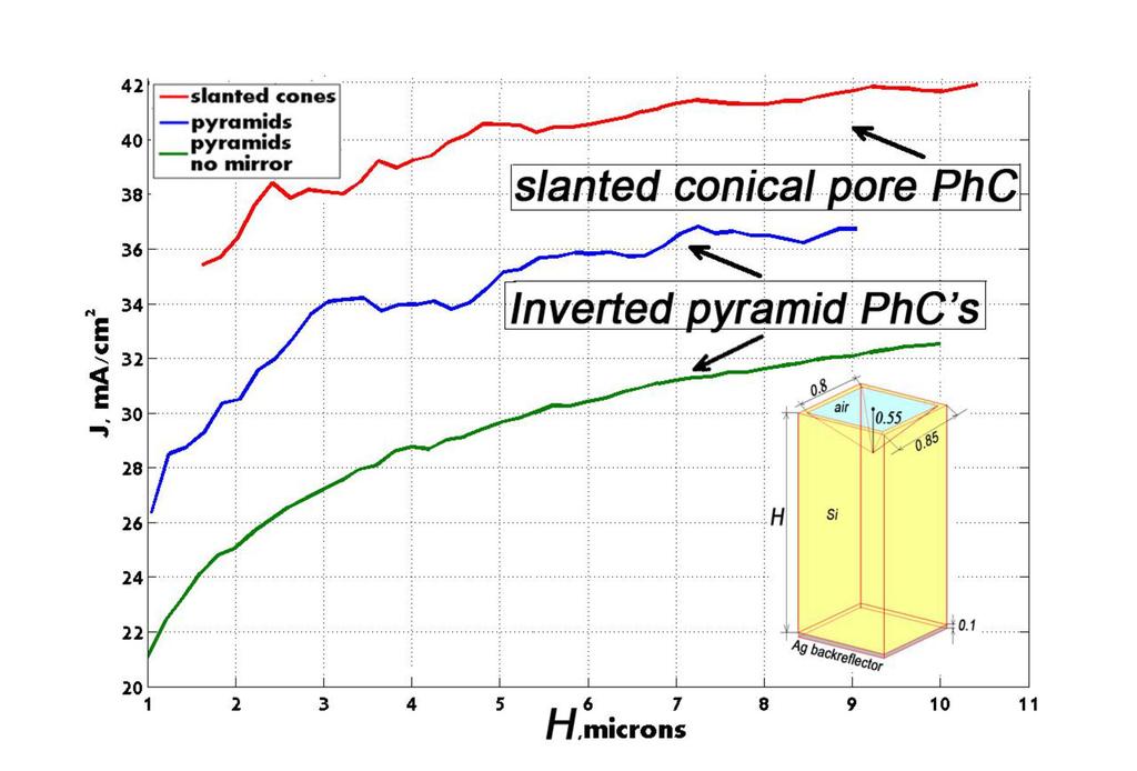
14 We examine the dependence of the MAPD on the silicon wafer thickness for intermediate values of H = 3-10μm (Fig. 5). For this purpose, we fix the lattice constant a=850nm (the optimal value found for the slanted conical PhC), keeping the minimal possible distance between the sides of pyramids equal d=100nm. For a=850nm, the MAPD demonstrates a gradual increase with wafer thickness but begins to saturate when the overall thickness H 5μm. We compare the MAPD dependence on the silicon wafer thickness, H, for three cases: 1) with no silver back-reflector (the PhC is placed on an infinite glass substrate), 2) with silver back-reflector (see Fig.2b), and 3) mathematically optimized slanted conical pore PhC with the lattice constant a=850nm and base radius r=500nm [7], placed on a silver back-reflector (Fig.1). For the specific choice of a=850nm, the slanted conical pore PhC (red curve) exhibits better performance than wet-etched structure of the same overall height H by about 3-5mA/cm 2. We find a MAPD J=35.5 ma/cm 2 in the spectral range of nm for H=h=1.6μm wafer thickness, which corresponds just 1μm effective bulk thickness of silicon [7]. As the thickness of slanted pore PhC is increased to H=10μm (h remains equal 1.6μm) the MAPD reaches almost J=42 ma/cm 2, only slightly below the perfect solar absorption value of 43.5 ma/cm 2. For the inverted pyramid PhC with lattice constant a=850nm (Fig.5 blue curve), when the overall height H=1.6μm (1.43μm equivalent bulk thickness) the 14
15 MAPD is about J=29 ma/cm 2. As the wafer thickness H increases, the MAPD reaches almost J=37 ma/cm 2 at H= 9μm. This is just slightly below the MAPD for a 300μm thick wafer with the same lattice periodicity. For calibration purposes and to delineate the role of the silver back-reflector, we also calculate the dependence of the MAPD on H for an inverted pyramid PhC s (with a=850nm) sitting on a semi-infinite glass substrate (green curve). In this case the MAPD reaches only J=32.5 ma/cm 2 for H=10μm. Fig.5 Short circuit current dependence (normal incidence of AM 1.5 sunlight) on the height H of silicon wafer, with a=850nm and pyramid depth h=550nm, for three cases: 1) Inverted pyramids with no silver back-reflector (the structure is placed on an infinite glass substrate), 2) Inverted pyramids placed on a silver back-reflector (see the inset), 3) Slanted conical pores of depth 1.6 microns with the lattice constant a=850nm, base radius r=500nm and silver backreflector. 15
16 For inverted pyramid PhC s, the optimal lattice constant is considerably larger than for the slanted conical pore PhC. Substantial improvements in the MAPD for H=3, 5 and 10μm thick inverted pyramid PC s are found when a is increased to 1.3μm, 1.9μm and 2.5μm respectively (see Fig.6). Fig.6 MAPD (normal incidence of AM 1.5 sunlight) dependence on lattice constant for inverted pyramid PhC s in bulk silicon, arranged in a square lattice and filled with air for three silicon heights. The structures are placed on silver back-reflectors. The distance between the sides of pyramids is 100nm. Maximal short circuit current obtained is J = 35.5 ma/cm 2 for H=3μm and a=1.3μm, J = 37.8 ma/cm 2 for H=5μm and a=1900nm, and J=40mA/cm 2 for a=2.5μm and H=10μm in the spectral range of nm. For an inverted pyramid PhC with H=3μm (blue curve) the MAPD reaches its maximum of 35.5mA/cm 2 for a=1.3μm. In the case of H=5μm this maximum shifts to a=1.9μm and the MAPD J = 37.8 ma/cm 2. This latter value coincides with the 16
17 best MAPD achieved for a 300μm thick wafer patterned with inverse pyramids (see Fig.4). Finally, for H=10μm, the optimum lattice constant is a=2.5 μm, for which the MAPD of J = 40 ma/cm 2 is found. We also investigate the influence of an anti-reflection coating (ARC) on the MAPD. A thin layer of SiO 2 on the surface can provide additional antireflective properties and at the same time passivate the silicon surface from unwanted carrier recombination. In our simulations, we consider a conformal, non-absorbing coating with a refractive index n=1.45 (see the inset in Fig.7). Fig.7 The MAPD dependence on the conformal coating thickness z for inverted pyramids in silicon placed on a silver back-reflector. The coating, consisting of glass with the refractive index n=1.45, is schematically depicted in the inset. The 17
18 overall height of silicon is H=10μm and the lattice constant a=2.5 μm. The distance between the sides of silicon pyramids is 100nm. Maximal short circuit current obtained is J = 41.1 ma/cm 2 for z=200nm. We consider the best case achieved in Fig.6. Namely, the overall height of the structure is H=10μm and the lattice constant a=2.5 μm. For these parameters the MAPD of J = 40 ma/cm 2 is found. It is seen that the MAPD increases with glass coating thickness, z, and reaches its maximum of 41.1mA/cm 2 for z=200nm. By including this antireflective passivation layer, we gain an additive contribution of 1.1 ma/cm 2 to solar cell performance. Furthermore, if the spacing between the sides of pyramids of 100nm is removed (d=0), we attain a MAPD of 42.5 ma/cm 2. Conclusion In conclusion, we have identified a set of intermediate thickness (3-10μm) silicon photonic crystals that enable strong light-trapping and solar absorption in the nm wavelength range. These structures require one to two orders of magnitude less silicon than conventional silicon solar cells used today, but provide a maximum achievable photocurrent density comparable to or even better than their much thicker counterparts. Our intermediate thickness photonic crystals are amenable to large scale fabrication by wet-etching, making them an attractive alternative to previously identified (mathematically optimum) structures consisting of a lattice of slanted conical pores. Unlike, the slanted conical pores that require a 18
19 curved surface profile, our intermediate thickness, inverted pyramid structures involve flat (111) and (100) surfaces of silicon. Our best 10-micron thick inverted pyramid PhC offers a MAPD of 40 ma/cm 2, compared to the corresponding slanted conical pore PhC with the MAPD of 42mA/cm 2 and compared to the perfect solar absorption limit of 43.5mA/cm 2. With a suitable surface passivation layer, an additive 1.1 ma/cm 2 is obtained for the inverted pyramid PhC. When the spacing between the sides of the inverted pyramids is removed (d=0 in Fig 2), we gain an additional 1.4 ma/cm 2 to reach our best MAPD of 42.5 ma/cm 2 for a 10- micron-height inverted-pyramid silicon photonic crystal. Even higher MAPD is expected for slanted-conical-pore photonic crystals of comparable thickness. These results are obtained by studying a relatively unexplored regime of thickness where novel wave effects and light trapping phenomena, remarkably, enable better solar absorption than in a 300 micron thick silicon solar cell. Given, the shorter carrier diffusion length required in a 10 micron thick silicon PhC solar cell, it is anticipated that this architecture may provide higher power conversion efficiency than currently employed thick ( μm) silicon solar cells. A recent study of black silicon [34] shows that surface recombination velocities can be reduced to ~ 10 cm/sec if the silicon surface is treated by conformal atomic layer deposition of Al 2 O 3. These results suggests that using a factor of 30 less active material, intermediate thickness silicon photonic crystals can approach and possibly surpass 19
20 the current world record power conversion efficiency (of about 25%) for silicon solar cells. Acknowledgements: S.E. and S.J. acknowledge support from the United States Department of Energy through contract DE-FG02-06ER KAU co-authors were funded by the Deanship of Scientific Research (DSR), King Abdulaziz University (KAU) under grant No. ( HiCi) and acknowledge technical and financial support of KAU. 4. Reference 1. S. John, "Electromagnetic Absorption in a Disordered Medium near a Photon Mobility Edge", Phys. Rev. Lett. 53, 2169 (1984). 2. S. John, "Strong Localization of Photons in Certain Disordered Dielectric Superlattices", Phys. Rev. Lett. 58, 2486 (1987). 3. E. Yablonovitch, Inhibited Spontaneous Emission in Solid-State Physics and Electronics, Phys. Rev. Lett. 58, 2059 (1987). 4. S. John and R. Rangarajan, "Optimal Structures for Classical Wave Localization: An Alternative to the Ioffe-Regel Criterion", Phys. Rev. B38, (1988). 5. Alongkarn Chutinan and Sajeev John, "Light trapping and absorption optimization in certain thin-film photonic crystal architectures", Physical Review A 78, (2008). 6. G. Demesy and S. John, Solar energy trapping with modulated silicon nanowire photonic crystals, J. Appl. Phys., 112, , (2012). 7. S. Eyderman, Sajeev John, and Alexei Deinega, Solar light trapping in slanted conical-pore photonic crystals: Beyond statistical ray trapping, J. Appl. Phys. 113, (2013). 8. S. Eyderman, Alexei Deinega and Sajeev John, Near perfect solar absorption in ultra-thin-film GaAs photonic crystals, J. Mater. Chem. A, 2, , (2014). 9. A. Deinega and S. John, J. Appl. Phys. 112, (2012) "Solar power conversion efficiency in modulated silicon nanowire photonic crystals". 20
21 10. A. Deinega, S. Eyderman, and S. John, Coupled optical and electrical modeling of solar cell based on conical pore silicon photonic crystals, J. Appl. Phys. 113, (2013). 11. Xingyu Zhang, Amir Hosseini, Polymer-based Hybrid Integrated Photonic Devices for Silicon On-chip Modulation and Board-level Optical Interconnects," Selected Topics in Quantum Electronics, IEEE Journal of, vol.19, no.6, pp (2013). 12. Jiali Yu et al.,"characterization and application of chirped photonic crystal fiber in multiphoton imaging," Optics Express, Vol. 22, Issue 9, pp (2014). 13. Xingyu Zhang et al., "Integrated Photonic Electromagnetic Field Sensor Based on Broadband Bowtie Antenna Coupled Silicon Organic Hybrid Modulator," IEEE Journal of Lightwave Technology, vol.32, no.20, pp (2014) 14. A. Al-Rashid and S. John, Optical Bio-sensing of Multiple Disease Markers in a Photonic-Band-Gap Lab-on-a-Chip: A Conceptual Paradigm, Phys. Rev. Applied 3, (2015). 15. T. Saga, Advances in crystalline silicon solar cell technology for industrial mass production, NPG Asia Mater. 2 (3) 96 (2010). 16. Green M. A., The path to 25% silicon solar cell efficiency: History of silicon cell evolution, Progress in Photovoltaics: Research and Applications, 17, , (2009). 17. P. Campbell, M. Green, Light trapping properties of pyramidally textured surfaces, Journal of Applied Physics, 52, pp , (1987). 18. F.-J. Haug et al., Resonances and absorption enhancement in thin film silicon solar cells with periodic interface texture, J. Appl. Phys. 109, (2011). 19. A. Deinega, I. Valuev, B. Potapkin, and Yu. Lozovik, Minimizing light reflection from dielectric textured surfaces, JOSA A 28, pp (2011). 20. Peter Bermel, Chiyan Luo, Lirong Zeng, Lionel C. Kimerling, and John D. Joannopoulos, Improving thin-film crystalline silicon solar cell efficiencies with photonic crystals, OPTICS EXPRESS, Vol. 15, No. 25, (2007). 21. J. Gjessing et al., Comparison of periodic light-trapping structures in thin crystalline silicon solar cells, J. Appl. Phys. 110, (2011). 22. E. Garnett and P. Yang, Light trapping in silicon nanowire solar cells, Nano Lett. 10(3), (2010). 23. Ping Kuang, Alexei Deinega, Mei-Li Hsieh, Sajeev John and Shawn-Yu Lin Light trapping and near-unity solar absorption in a three-dimensional photoniccrystal", Optics Letters 38, No. 20, 4200 (2013). 21
22 24. Xing Sheng, Lirong Z. Broderick, Lionel C. Kimerling, Photonic crystal structures for light trapping in thin-film Si solar cells: Modeling, process and optimizations, Volume 314,Pages 41 47, (2014). 25. X. H. Li et al., Light trapping in thin-film solar cells via scattering by nanostructured antireflection coatings, JOURNAL OF APPLIED PHYSICS, 114, (2013). 26. X. Li, et al., "Subwavelength nanostructures integrated with polymerpackaged III-V solar cells for omnidirectional, broad-spectrum improvement of photovoltaic performance," Prog. Photovolt: Res. Appl. DOI: /pip.2565 (2014). 27. Hsin-Han Lin and Wen-Hwa Chen, "Improvement of polycrystalline silicon wafer solar cell efficiency by forming nanoscale pyramids on wafer surface using a self-mask etching technique", J Vac Sci Technol B Nanotechnol Microelectron., 31(3), , (2013). 28. T. Deng, J. Chen, C. N. Wu, and Z. W. Liu, "Fabrication of Inverted-Pyramid Silicon Nanopore Arrays with Three-Step Wet Etching", ECS Journal of Solid State Science and Technology, 2(11), pp , (2013). 29. A. Taflove and S. C. Hagness, Computational Electrodynamics: The Finite- Difference Time-Domain Method, 3rd ed. (Artech House Publishers, 2005). 30. See for Electromagnetic Template Library (EMTL), Kintech Lab Ltd. 31. A. Deinega and S. John, Effective optical response of silicon to sunlight in the finite-difference time-domain method, Opt. Lett. 37, 112 (2012). 32. See for Fitting of dielectric function. 33. See for Reference Solar Spectral Irradiance: Air Mass Hele Savin et al., Black silicon solar cells with interdigitated back-contacts achieve 22.1% efficiency, Nature Nanotechnology, DOI: /NNANO
23
24
25
26
27
28
29
Nanophotonics: solar and thermal applications
 Nanophotonics: solar and thermal applications Shanhui Fan Ginzton Laboratory and Department of Electrical Engineering Stanford University http://www.stanford.edu/~shanhui Nanophotonic Structures Photonic
PHOTOVOLTAICS Fundamentals
 PHOTOVOLTAICS Fundamentals PV FUNDAMENTALS Semiconductor basics pn junction Solar cell operation Design of silicon solar cell SEMICONDUCTOR BASICS Allowed energy bands Valence and conduction band Fermi
(Co-PIs-Mark Brongersma, Yi Cui, Shanhui Fan) Stanford University. GCEP Research Symposium 2013 Stanford, CA October 9, 2013
 Stanford University. GCEP Research Symposium 2013 Stanford, CA October 9, 2013") High-efficiency thin film nano-structured multi-junction solar James S. cells Harris (PI) (Co-PIs-Mark Brongersma, Yi Cui, Shanhui Fan) Stanford University GCEP Research Symposium 2013 Stanford, CA October
High-efficiency thin film nano-structured multi-junction solar James S. cells Harris (PI) (Co-PIs-Mark Brongersma, Yi Cui, Shanhui Fan) Stanford University GCEP Research Symposium 2013 Stanford, CA October
Demonstration of Near-Infrared Negative-Index Materials
 Demonstration of Near-Infrared Negative-Index Materials Shuang Zhang 1, Wenjun Fan 1, N. C. Panoiu 2, K. J. Malloy 1, R. M. Osgood 2 and S. R. J. Brueck 2 1. Center for High Technology Materials and Department
Fundamentals of Light Trapping
 Fundamentals of Light Trapping James R. Nagel, PhD November 16, 2017 Salt Lake City, Utah About Me PhD, Electrical Engineering, University of Utah (2011) Research Associate for Dept. of Metallurgical Engineering
Bulk crystalline silicon (c-si) solar cells dominate the
 solar cells dominate the") pubs.acs.org/nanolett Efficient Light Trapping in Inverted Nanopyramid Thin Crystalline Silicon Membranes for Solar Cell Applications Anastassios Mavrokefalos, Sang Eon Han, Selcuk Yerci, Matthew S. Branham,
pubs.acs.org/nanolett Efficient Light Trapping in Inverted Nanopyramid Thin Crystalline Silicon Membranes for Solar Cell Applications Anastassios Mavrokefalos, Sang Eon Han, Selcuk Yerci, Matthew S. Branham,
Organic Solar Cell: Optics in Smooth and Pyramidal Rough Surface
 IOSR Journal of Electrical and Electronics Engineering (IOSR-JEEE) e-issn: 2278-1676,p-ISSN: 2320-3331, Volume 10, Issue 4 Ver. III (July Aug. 2015), PP 67-72 www.iosrjournals.org Organic Solar Cell: Optics
Efficient Light Trapping in Inverted Nanopyramid Thin Crystalline Silicon Membranes for Solar Cell Applications
 Efficient Light Trapping in Inverted Nanopyramid Thin Crystalline Silicon Membranes for Solar Cell Applications The MIT Faculty has made this article openly available. Please share how this access benefits
Research on the Wide-angle and Broadband 2D Photonic Crystal Polarization Splitter
 Progress In Electromagnetics Research Symposium 2005, Hangzhou, China, August 22-26 551 Research on the Wide-angle and Broadband 2D Photonic Crystal Polarization Splitter Y. Y. Li, P. F. Gu, M. Y. Li,
Light trapping in ultrathin silicon photonic crystal superlattices with randomly-textured dielectric incouplers
 Light trapping in ultrathin silicon photonic crystal superlattices with randomly-textured dielectric incouplers Dennis M. Callahan, 1,* Kelsey A. W. Horowitz, 1 and Harry A. Atwater 1 1 Thomas J. Watson
3.1 Introduction to Semiconductors. Y. Baghzouz ECE Department UNLV
 3.1 Introduction to Semiconductors Y. Baghzouz ECE Department UNLV Introduction In this lecture, we will cover the basic aspects of semiconductor materials, and the physical mechanisms which are at the
Graded S i N x /S i O x N y Layers as Antireflective Coatings for Solar Cells Based on GaAs and Silicon Crystalline
 Science Research 2016; 4(1): 21-25 Published online February 25, 2016 (http://www.sciencepublishinggroup.com/j/sr) doi: 10.11648/j.sr.20160401.14 ISSN: 2329-0935 (Print); ISSN: 2329-0927 (Online) Graded
Nanostrukturphysik (Nanostructure Physics)
") Nanostrukturphysik (Nanostructure Physics) Prof. Yong Lei & Dr. Yang Xu Fachgebiet 3D-Nanostrukturierung, Institut für Physik Contact: yong.lei@tu-ilmenau.de; yang.xu@tu-ilmenau.de Office: Unterpoerlitzer
Nanostrukturphysik (Nanostructure Physics) Prof. Yong Lei & Dr. Yang Xu Fachgebiet 3D-Nanostrukturierung, Institut für Physik Contact: yong.lei@tu-ilmenau.de; yang.xu@tu-ilmenau.de Office: Unterpoerlitzer
A Novel Design of Photonic Crystal Lens Based on Negative Refractive Index
 PIERS ONLINE, VOL. 4, NO. 2, 2008 296 A Novel Design of Photonic Crystal Lens Based on Negative Refractive Index S. Haxha 1 and F. AbdelMalek 2 1 Photonics Group, Department of Electronics, University
Nanomaterials and their Optical Applications
 Nanomaterials and their Optical Applications Winter Semester 2012 Lecture 08 rachel.grange@uni-jena.de http://www.iap.uni-jena.de/multiphoton Outline: Photonic crystals 2 1. Photonic crystals vs electronic
Optimizing the performance of metal-semiconductor-metal photodetectors by embedding nanoparticles in the absorption layer
 Journal of Electrical and Electronic Engineering 2015; 3(2-1): 78-82 Published online February 10, 2015 (http://www.sciencepublishinggroup.com/j/jeee) doi: 10.11648/j.jeee.s.2015030201.27 ISSN: 2329-1613
Tooth-shaped plasmonic waveguide filters with nanometeric. sizes
 Tooth-shaped plasmonic waveguide filters with nanometeric sizes Xian-Shi LIN and Xu-Guang HUANG * Laboratory of Photonic Information Technology, South China Normal University, Guangzhou, 510006, China
FINITE DIFFERENCE TIME DOMAIN SIMULATION OF LIGHT TRAPPING IN A GaAs COMPLEX STRUCTURE
 Romanian Reports in Physics 70, XYZ (2018) FINITE DIFFERENCE TIME DOMAIN SIMULATION OF LIGHT TRAPPING IN A GaAs COMPLEX STRUCTURE MOHAMMED M. SHABAT 1, NADARA S. El-SAMAK 1, DANIEL M. SCHAADT 2 1 Physics
Supplemental Discussion for Multijunction Solar Cell Efficiencies: Effect of Spectral Window, Optical Environment and Radiative Coupling
 Electronic Supplementary Material (ESI) for Energy & Environmental Science. This journal is The Royal Society of Chemistry 2014 Supplemental Discussion for Multijunction Solar Cell Efficiencies: Effect
TUNABLE MULTI-CHANNEL FILTERING USING 1-D PHOTONIC QUANTUM WELL STRUCTURES
 Progress In Electromagnetics Research Letters, Vol. 27, 43 51, 2011 TUNABLE MULTI-CHANNEL FILTERING USING 1-D PHOTONIC QUANTUM WELL STRUCTURES B. Suthar * and A. Bhargava Nanophysics Laboratory, Department
Chapter 5. Effects of Photonic Crystal Band Gap on Rotation and Deformation of Hollow Te Rods in Triangular Lattice
 Chapter 5 Effects of Photonic Crystal Band Gap on Rotation and Deformation of Hollow Te Rods in Triangular Lattice In chapter 3 and 4, we have demonstrated that the deformed rods, rotational rods and perturbation
FINITE-DIFFERENCE FREQUENCY-DOMAIN ANALYSIS OF NOVEL PHOTONIC
 FINITE-DIFFERENCE FREQUENCY-DOMAIN ANALYSIS OF NOVEL PHOTONIC WAVEGUIDES Chin-ping Yu (1) and Hung-chun Chang (2) (1) Graduate Institute of Electro-Optical Engineering, National Taiwan University, Taipei,
Absorption enhancement in double-sided nanocone hole arrays for solar cells
 University of Wollongong Research Online Faculty of Engineering and Information Sciences - Papers: Part A Faculty of Engineering and Information Sciences 2015 Absorption enhancement in double-sided nanocone
High efficiency solar cells by nanophotonic design
 High efficiency solar cells by nanophotonic design Piero Spinelli Claire van Lare Jorik van de Groep Bonna Newman Mark Knight Paula Bronsveld Frank Lenzmann Ruud Schropp Wim Sinke Albert Polman Center
Supplementary Information
 Electronic Supplementary Material (ESI) for Nanoscale. This journal is The Royal Society of Chemistry 2014 Supplementary Information Large-scale lithography-free metasurface with spectrally tunable super
DIELECTRIC nanoparticles (NPs) have recently been proposed
 have recently been proposed") IEEE JOURNAL OF PHOTOVOLTAICS 1 Effect of EVA Encapsulation on Antireflection Properties of Mie Nanoscatterers for c-si Solar Cells P. Spinelli, F. Lenzmann, A. Weeber, and A. Polman Abstract Dielectric
IEEE JOURNAL OF PHOTOVOLTAICS 1 Effect of EVA Encapsulation on Antireflection Properties of Mie Nanoscatterers for c-si Solar Cells P. Spinelli, F. Lenzmann, A. Weeber, and A. Polman Abstract Dielectric
Graded SiO x N y layers as antireflection coatings for solar cells application
 Materials Science-Poland, Vol. 24, No. 4, 2006 Graded SiO x N y layers as antireflection coatings for solar cells application M. LIPIŃSKI 1*, S. KLUSKA 2, H. CZTERNASTEK 2, P. ZIĘBA 1 1 Institute of Metallurgy
Simulations of solar cell absorption enhancement using resonant modes of a nanosphere array
 Green Photonics Award Paper Simulations of solar cell absorption enhancement using resonant modes of a nanosphere array Jonathan Grandidier* a, Michael G. Deceglie a, Dennis M. Callahan a, Harry A. Atwater
Nanoscale optical circuits: controlling light using localized surface plasmon resonances
 Nanoscale optical circuits: controlling light using localized surface plasmon resonances T. J. Davis, D. E. Gómez and K. C. Vernon CSIRO Materials Science and Engineering Localized surface plasmon (LSP)
Introduction to Semiconductor Integrated Optics
 Introduction to Semiconductor Integrated Optics Hans P. Zappe Artech House Boston London Contents acknowledgments reface itroduction Chapter 1 Basic Electromagnetics 1 1.1 General Relationships 1 1.1.1
U-Shaped Nano-Apertures for Enhanced Optical Transmission and Resolution
 U-Shaped Nano-Apertures for Enhanced Optical Transmission and Resolution Mustafa Turkmen 1,2,3, Serap Aksu 3,4, A. Engin Çetin 2,3, Ahmet A. Yanik 2,3, Alp Artar 2,3, Hatice Altug 2,3,4, * 1 Electrical
The Electromagnetic Properties of Materials
 The Electromagnetic Properties of Materials Electrical conduction Metals Semiconductors Insulators (dielectrics) Superconductors Magnetic materials Ferromagnetic materials Others Photonic Materials (optical)
Plasmonic fractals: ultrabroadband light trapping in thin film solar cells by a Sierpinski nanocarpet
 Plasmonic fractals: ultrabroadband light trapping in thin film solar cells by a Sierpinski nanocarpet Hanif Kazerooni 1, Amin Khavasi, 2,* 1. Chemical Engineering Faculty, Amirkabir University of Technology
Supporting information. Unidirectional Doubly Enhanced MoS 2 Emission via
 Supporting information Unidirectional Doubly Enhanced MoS 2 Emission via Photonic Fano Resonances Xingwang Zhang, Shinhyuk Choi, Dake Wang, Carl H. Naylor, A. T. Charlie Johnson, and Ertugrul Cubukcu,,*
Wideband enhancement of infrared absorption in a direct band-gap semiconductor by using nonabsorptive pyramids
 Wideband enhancement of infrared absorption in a direct band-gap semiconductor by using nonabsorptive pyramids The MIT Faculty has made this article openly available. Please share how this access benefits
Light trapping in thin-film solar cells: the role of guided modes
 Light trapping in thin-film solar cells: the role of guided modes T. Søndergaard *, Y.-C. Tsao, T. G. Pedersen, and K. Pedersen Department of Physics and Nanotechnology, Aalborg University, Skjernvej 4A,
Superconductivity Induced Transparency
 Superconductivity Induced Transparency Coskun Kocabas In this paper I will discuss the effect of the superconducting phase transition on the optical properties of the superconductors. Firstly I will give
Terahertz antireflection coating enabled by a subwavelength metallic mesh capped with a thin dielectric film
 Invited Paper Terahertz antireflection coating enabled by a subwavelength metallic mesh capped with a thin dielectric film Li Huang 1*, Beibei Zeng 2, Chun-Chieh Chang 2 and Hou-Tong Chen 2* 1 Physics
High resolution THz scanning for optimization of dielectric layer opening process on doped Si surfaces
 High resolution THz scanning for optimization of dielectric layer opening process on doped Si surfaces P. Spinelli 1, F.J.K. Danzl 1, D. Deligiannis 1,2, N. Guillevin 1, A.R. Burgers 1, S. Sawallich 3,
SURFACE PLASMONS AND THEIR APPLICATIONS IN ELECTRO-OPTICAL DEVICES
 SURFACE PLASMONS AND THEIR APPLICATIONS IN ELECTRO-OPTICAL DEVICES Igor Zozouleno Solid State Electronics Department of Science and Technology Linöping University Sweden igozo@itn.liu.se http://www.itn.liu.se/meso-phot
Polarization control and sensing with two-dimensional coupled photonic crystal microcavity arrays. Hatice Altug * and Jelena Vučković
 Polarization control and sensing with two-dimensional coupled photonic crystal microcavity arrays Hatice Altug * and Jelena Vučković Edward L. Ginzton Laboratory, Stanford University, Stanford, CA 94305-4088
transmission reflection absorption
 Optical Cages V. Kumar*, J. P. Walker* and H. Grebel The Electronic Imaging Center and the ECE department at NJIT, Newark, NJ 0702. grebel@njit.edu * Contributed equally Faraday Cage [], a hollow structure
Plasmon enhancement of optical absorption in ultra-thin film solar cells by rear located aluminum nanodisk arrays
 Opt Quant Electron (2017)49:161 DOI 10.1007/s11082-017-0930-x Plasmon enhancement of optical absorption in ultra-thin film solar cells by rear located aluminum nanodisk arrays Debao Zhang 1 Yawei Kuang
Introduction to Photonic Crystals
 1 Introduction to Photonic Crystals Summary. Chapter 1 gives a brief introduction into the basics of photonic crystals which are a special class of optical media with periodic modulation of permittivity.
Band structure of honeycomb photonic crystal slabs
 JOURNAL OF APPLIED PHYSICS 99, 093102 2006 Band structure of honeycomb photonic crystal slabs Tai-I Weng and G. Y. Guo a Department of Physics, National Taiwan University, Taipei, Taiwan 106, Republic
Photonic band gaps with layer-by-layer double-etched structures
 Photonic band gaps with layer-by-layer double-etched structures R. Biswas a) Microelectronics Research Center, Ames Laboratory USDOE and Department of Physics and Astronomy, Iowa State University, Ames,
ECE 695 Numerical Simulations Lecture 35: Solar Hybrid Energy Conversion Systems. Prof. Peter Bermel April 12, 2017
 ECE 695 Numerical Simulations Lecture 35: Solar Hybrid Energy Conversion Systems Prof. Peter Bermel April 12, 2017 Ideal Selective Solar Absorber Efficiency Limits Ideal cut-off wavelength for a selective
EE495/695 Introduction to Semiconductors I. Y. Baghzouz ECE Department UNLV
 EE495/695 Introduction to Semiconductors I Y. Baghzouz ECE Department UNLV Introduction Solar cells have always been aligned closely with other electronic devices. We will cover the basic aspects of semiconductor
Theoretical Study on Graphene Silicon Heterojunction Solar Cell
 Copyright 2015 American Scientific Publishers All rights reserved Printed in the United States of America Journal of Nanoelectronics and Optoelectronics Vol. 10, 1 5, 2015 Theoretical Study on Graphene
Progress In Electromagnetics Research Letters, Vol. 42, 13 22, 2013
 Progress In Electromagnetics Research Letters, Vol. 42, 3 22, 23 OMNIDIRECTIONAL REFLECTION EXTENSION IN A ONE-DIMENSIONAL SUPERCONDUCTING-DIELECTRIC BINARY GRADED PHOTONIC CRYSTAL WITH GRADED GEOMETRIC
Negative Index of Refraction in Optical Metamaterials
 1 Negative Index of Refraction in Optical Metamaterials V. M. Shalaev, W. Cai, U. Chettiar, H.-K. Yuan, A. K. Sarychev, V. P. Drachev, and A. V. Kildishev School of Electrical and Computer Engineering,
Citation for published version (APA): Shen, C. (2006). Wave Propagation through Photonic Crystal Slabs: Imaging and Localization. [S.l.]: s.n.
![Citation for published version (APA): Shen, C. (2006). Wave Propagation through Photonic Crystal Slabs: Imaging and Localization. [S.l.]: s.n.](/thumbs/95/124821987.jpg "Citation for published version (APA): Shen, C. (2006). Wave Propagation through Photonic Crystal Slabs: Imaging and Localization. [S.l.]: s.n.") University of Groningen Wave Propagation through Photonic Crystal Slabs Shen, Chuanjian IMPORTANT NOTE: You are advised to consult the publisher's version (publisher's PDF) if you wish to cite from it.
University of Groningen Wave Propagation through Photonic Crystal Slabs Shen, Chuanjian IMPORTANT NOTE: You are advised to consult the publisher's version (publisher's PDF) if you wish to cite from it.
Supplementary Figure 1 Schematics of an optical pulse in a nonlinear medium. A Gaussian optical pulse propagates along z-axis in a nonlinear medium
 Supplementary Figure 1 Schematics of an optical pulse in a nonlinear medium. A Gaussian optical pulse propagates along z-axis in a nonlinear medium with thickness L. Supplementary Figure Measurement of
PHYSICS nd TERM Outline Notes (continued)
") PHYSICS 2800 2 nd TERM Outline Notes (continued) Section 6. Optical Properties (see also textbook, chapter 15) This section will be concerned with how electromagnetic radiation (visible light, in particular)
PHYSICS 2800 2 nd TERM Outline Notes (continued) Section 6. Optical Properties (see also textbook, chapter 15) This section will be concerned with how electromagnetic radiation (visible light, in particular)
Self-assembled nanostructures for antireflection optical coatings
 Self-assembled nanostructures for antireflection optical coatings Yang Zhao 1, Guangzhao Mao 2, and Jinsong Wang 1 1. Deaprtment of Electrical and Computer Engineering 2. Departmentof Chemical Engineering
Flexible Organic Photovoltaics Employ laser produced metal nanoparticles into the absorption layer 1. An Introduction
 Flexible Organic Photovoltaics Employ laser produced metal nanoparticles into the absorption layer 1. An Introduction Among the renewable energy sources that are called to satisfy the continuously increased
Chapter 7. Solar Cell
 Chapter 7 Solar Cell 7.0 Introduction Solar cells are useful for both space and terrestrial application. Solar cells furnish the long duration power supply for satellites. It converts sunlight directly
A. K. Das Department of Physics, P. K. College, Contai; Contai , India.
 IOSR Journal of Applied Physics (IOSR-JAP) e-issn: 2278-4861.Volume 7, Issue 2 Ver. II (Mar. - Apr. 2015), PP 08-15 www.iosrjournals.org Efficiency Improvement of p-i-n Structure over p-n Structure and
Photonic crystal with multiple-hole defect for sensor applications
 Photonic crystal with multiple-hole defect for sensor applications Christopher Kang 1,* and Sharon M. Weiss 1,2 1 Interdisciplinary Graduate Program in Materials Science, Vanderbilt University, Nashville,
Multi-cycle THz pulse generation in poled lithium niobate crystals
 Laser Focus World April 2005 issue (pp. 67-72). Multi-cycle THz pulse generation in poled lithium niobate crystals Yun-Shik Lee and Theodore B. Norris Yun-Shik Lee is an assistant professor of physics
High Efficiency Triple-Junction Solar Cells Employing Biomimetic Antireflective Structures
 High Efficiency Triple-Junction Solar Cells Employing Biomimetic Antireflective Structures M.Y. Chiu, C.-H. Chang, F.-Y. Chang, and Peichen Yu, Green Photonics Laboratory Department of Photonics National
Nanomaterials and their Optical Applications
 Nanomaterials and their Optical Applications Winter Semester 2013 Lecture 02 rachel.grange@uni-jena.de http://www.iap.uni-jena.de/multiphoton Lecture 2: outline 2 Introduction to Nanophotonics Theoretical
Research Article Si Substrate-Based Metamaterials for Ultrabroadband Perfect Absorption in Visible Regime
 Nanomaterials, Article ID 893202, 5 pages http://dx.doi.org/0.55/204/893202 Research Article Si Substrate-Based Metamaterials for Ultrabroadband Perfect in Visible Regime Qi Han, Lei Jin, Yongqi Fu, and
l* = 109 nm Glycerol Clean Water Glycerol l = 108 nm Wavelength (nm)
") 1/ (rad -1 ) Normalized extinction a Clean 0.8 Water l* = 109 nm 0.6 Glycerol b 2.0 1.5 500 600 700 800 900 Clean Water 0.5 Glycerol l = 108 nm 630 660 690 720 750 Supplementary Figure 1. Refractive index
1/ (rad -1 ) Normalized extinction a Clean 0.8 Water l* = 109 nm 0.6 Glycerol b 2.0 1.5 500 600 700 800 900 Clean Water 0.5 Glycerol l = 108 nm 630 660 690 720 750 Supplementary Figure 1. Refractive index
Backscattering enhancement of light by nanoparticles positioned in localized optical intensity peaks
 Backscattering enhancement of light by nanoparticles positioned in localized optical intensity peaks Zhigang Chen, Xu Li, Allen Taflove, and Vadim Backman We report what we believe to be a novel backscattering
Embedded metallic nanopatterns for enhanced optical absorption
 Embedded metallic nanopatterns for enhanced optical absorption Fan Ye, Michael J. Burns, Michael J. Naughton* Department of Physics, Boston College, Chestnut Hill MA 02467 ABSTRACT Novel metallic nanopatterns
Third generation solar cells - How to use all the pretty colours?
 Third generation solar cells - How to use all the pretty colours? Erik Stensrud Marstein Department for Solar Energy Overview The trouble with conventional solar cells Third generation solar cell concepts
Dielectric Meta-Reflectarray for Broadband Linear Polarization Conversion and Optical Vortex Generation
 Supporting Information Dielectric Meta-Reflectarray for Broadband Linear Polarization Conversion and Optical Vortex Generation Yuanmu Yang, Wenyi Wang, Parikshit Moitra, Ivan I. Kravchenko, Dayrl P. Briggs,
The Broadband Fixed-Angle Source Technique (BFAST) LUMERICAL SOLUTIONS INC
 LUMERICAL SOLUTIONS INC") The Broadband Fixed-Angle Source Technique (BFAST) LUMERICAL SOLUTIONS INC. 1 Outline Introduction Lumerical s simulation products Simulation of periodic structures The new Broadband Fixed-Angle Source
The Broadband Fixed-Angle Source Technique (BFAST) LUMERICAL SOLUTIONS INC. 1 Outline Introduction Lumerical s simulation products Simulation of periodic structures The new Broadband Fixed-Angle Source
Polarization control of defect modes in threedimensional woodpile photonic crystals
 Polarization control of defect modes in threedimensional woodpile photonic crystals Michael James Ventura and Min Gu* Centre for Micro-Photonics and Centre for Ultrahigh-bandwidth Devices for Optical Systems,
Design and Characterization of a Dual-Band Metamaterial Absorber Based on Destructive Interferences
 Progress In Electromagnetics Research C, Vol. 47, 95, 24 Design and Characterization of a Dual-Band Metamaterial Absorber Based on Destructive Interferences Saeid Jamilan, *, Mohammad N. Azarmanesh, and
Electroluminescence from Silicon and Germanium Nanostructures
 Electroluminescence from silicon Silicon Getnet M. and Ghoshal S.K 35 ORIGINAL ARTICLE Electroluminescence from Silicon and Germanium Nanostructures Getnet Melese* and Ghoshal S. K.** Abstract Silicon
Design of a Multi-Mode Interference Crossing Structure for Three Periodic Dielectric Waveguides
 Progress In Electromagnetics Research Letters, Vol. 75, 47 52, 2018 Design of a Multi-Mode Interference Crossing Structure for Three Periodic Dielectric Waveguides Haibin Chen 1, Zhongjiao He 2,andWeiWang
Absorption suppression in photonic crystals
 PHYSICAL REVIEW B 77, 442 28 Absorption suppression in photonic crystals A. Figotin and I. Vitebskiy Department of Mathematics, University of California at Irvine, Irvine, California 92697, USA Received
Directional emitter and beam splitter based on self-collimation effect
 Directional emitter and beam splitter based on self-collimation effect W. Y. Liang, J. W. Dong, and H. Z. Wang* State Key Laboratory of Optoelectronic Materials and Technologies, Zhongshan (Sun Yat-Sen)
Nanostrukturphysik (Nanostructure Physics)
") Nanostrukturphysik (Nanostructure Physics) Prof. Yong Lei & Dr. Yang Xu Fachgebiet 3D-Nanostrukturierung, Institut für Physik Contact: yong.lei@tu-ilmenau.de; yang.xu@tu-ilmenau.de Office: Unterpoerlitzer
Nanostrukturphysik (Nanostructure Physics) Prof. Yong Lei & Dr. Yang Xu Fachgebiet 3D-Nanostrukturierung, Institut für Physik Contact: yong.lei@tu-ilmenau.de; yang.xu@tu-ilmenau.de Office: Unterpoerlitzer
Design of Plasmonic Nanoparticles for Efficient Subwavelength Light Trapping in Thin-Film Solar Cells
 Plasmonics (2011) 6:155 161 DOI 10.1007/s11468-010-9181-4 Design of Plasmonic Nanoparticles for Efficient Subwavelength Light Trapping in Thin-Film Solar Cells Yuriy A. Akimov Wee Shing Koh Received: 15
Title. Author(s)Nagasaki, Akira; Saitoh, Kunimasa; Koshiba, Masanori. CitationOptics Express, 19(4): Issue Date Doc URL.
Nagasaki, Akira; Saitoh, Kunimasa; Koshiba, Masanori. CitationOptics Express, 19(4): Issue Date Doc URL.") Title Polarization characteristics of photonic crystal fib Author(s)Nagasaki, Akira; Saitoh, Kunimasa; Koshiba, Masanori CitationOptics Express, 19(4): 3799-3808 Issue Date 2011-02-14 Doc URL http://hdl.handle.net/2115/45257
Title Polarization characteristics of photonic crystal fib Author(s)Nagasaki, Akira; Saitoh, Kunimasa; Koshiba, Masanori CitationOptics Express, 19(4): 3799-3808 Issue Date 2011-02-14 Doc URL http://hdl.handle.net/2115/45257
Surface plasmon waveguides
 Surface plasmon waveguides Introduction Size Mismatch between Scaled CMOS Electronics and Planar Photonics Photonic integrated system with subwavelength scale components CMOS transistor: Medium-sized molecule
6 Correlation between the surface morphology and the current enhancement in n-i-p silicon solar cells
 6 Correlation between the surface morphology and the current enhancement in n-i-p silicon solar cells 6.1 Introduction In order to enhance the generated photocurrent in thin microcrystalline silicon solar
Angular and polarization properties of a photonic crystal slab mirror
 Angular and polarization properties of a photonic crystal slab mirror Virginie Lousse 1,2, Wonjoo Suh 1, Onur Kilic 1, Sora Kim 1, Olav Solgaard 1, and Shanhui Fan 1 1 Department of Electrical Engineering,
Left-handed materials: Transfer matrix method studies
 Left-handed materials: Transfer matrix method studies Peter Markos and C. M. Soukoulis Outline of Talk What are Metamaterials? An Example: Left-handed Materials Results of the transfer matrix method Negative
Enhancing the Rate of Spontaneous Emission in Active Core-Shell Nanowire Resonators
 Chapter 6 Enhancing the Rate of Spontaneous Emission in Active Core-Shell Nanowire Resonators 6.1 Introduction Researchers have devoted considerable effort to enhancing light emission from semiconductors
Electrons are shared in covalent bonds between atoms of Si. A bound electron has the lowest energy state.
 Photovoltaics Basic Steps the generation of light-generated carriers; the collection of the light-generated carriers to generate a current; the generation of a large voltage across the solar cell; and
Strongly Localized Photonic Mode in 2D Periodic Structure Without Bandgap
 Strongly Localized Photonic Mode in D Periodic Structure Without Bandgap V. M. APALKOV M. E. RAIKH Physics Department, University of Utah The work was supported by: the Army Research Office under Grant
PLASMONIC LIGHT TRAPPING FOR THIN FILM A-SI:H SOLAR CELLS
 PLASMONIC LIGHT TRAPPING FOR THIN FILM A-SI:H SOLAR CELLS VIVIAN E. FERRY 1,2, MARC A. VERSCHUUREN 3, HONGBO B. T. LI 4, EWOLD VERHAGEN 1, ROBERT J. WALTERS 1, RUUD E. I. SCHROPP 4, HARRY A. ATWATER 2,
Supplementary Information Supplementary Figures
 Supplementary Information Supplementary Figures Supplementary Figure S1. Schematic defining the relevant physical parameters in our grating coupler model. The schematic shows a normally-incident light
Thermionic Current Modeling and Equivalent Circuit of a III-V MQW P-I-N Photovoltaic Heterostructure
 Thermionic Current Modeling and Equivalent Circuit of a III-V MQW P-I-N Photovoltaic Heterostructure ARGYRIOS C. VARONIDES Physics and Electrical Engineering Department University of Scranton 800 Linden
Sub-wavelength electromagnetic structures
 Sub-wavelength electromagnetic structures Shanhui Fan, Z. Ruan, L. Verselegers, P. Catrysse, Z. Yu, J. Shin, J. T. Shen, G. Veronis Ginzton Laboratory, Stanford University http://www.stanford.edu/group/fan
Model Answer (Paper code: AR-7112) M. Sc. (Physics) IV Semester Paper I: Laser Physics and Spectroscopy
 M. Sc. (Physics) IV Semester Paper I: Laser Physics and Spectroscopy") Model Answer (Paper code: AR-7112) M. Sc. (Physics) IV Semester Paper I: Laser Physics and Spectroscopy Section I Q1. Answer (i) (b) (ii) (d) (iii) (c) (iv) (c) (v) (a) (vi) (b) (vii) (b) (viii) (a) (ix)
Model Answer (Paper code: AR-7112) M. Sc. (Physics) IV Semester Paper I: Laser Physics and Spectroscopy Section I Q1. Answer (i) (b) (ii) (d) (iii) (c) (iv) (c) (v) (a) (vi) (b) (vii) (b) (viii) (a) (ix)
EE 446/646 Photovoltaic Devices I. Y. Baghzouz
 EE 446/646 Photovoltaic Devices I Y. Baghzouz What is Photovoltaics? First used in about 1890, the word has two parts: photo, derived from the Greek word for light, volt, relating to electricity pioneer
Photonic devices for quantum information processing:
 Outline Photonic devices for quantum information processing: coupling to dots, structure design and fabrication Optoelectronics Group, Cavendish Lab Outline Vuckovic s group Noda s group Outline Outline
Semiconductor Disk Laser on Microchannel Cooler
 Semiconductor Disk Laser on Microchannel Cooler Eckart Gerster An optically pumped semiconductor disk laser with a double-band Bragg reflector mirror is presented. This mirror not only reflects the laser
SUPPLEMENTARY INFORMATION
 SUPPLEMENTARY INFORMATION Supplementary Information I. Schematic representation of the zero- n superlattices Schematic representation of a superlattice with 3 superperiods is shown in Fig. S1. The superlattice
Analysis of waveguides coupling in Photonic Crystal Power-Splitter
 International Research Journal of Applied and Basic Sciences 204 Available online at www.irjabs.com ISSN 225-838X / Vol, 8 (9): 259-264 Science Explorer Publications Analysis of waveguides coupling in
Quantum Dot Technology for Low-Cost Space Power Generation for Smallsats
 SSC06-VI- Quantum Dot Technology for Low-Cost Space Power Generation for Smallsats Theodore G. DR Technologies, Inc. 7740 Kenamar Court, San Diego, CA 92020 (858)677-230 tstern@drtechnologies.com The provision
Limiting acceptance angle to maximize efficiency in solar cells
 Limiting acceptance angle to maximize efficiency in solar cells Emily D. Kosten a and Harry A. Atwater a,b a Thomas J. Watson Laboratories of Applied Physics, California Institute of Technology, Pasadena,
Analyze the effect of window layer (AlAs) for increasing the efficiency of GaAs based solar cell
 for increasing the efficiency of GaAs based solar cell") American Journal of Engineering Research (AJER) e-issn: 2320-0847 p-issn : 2320-0936 Volume-4, Issue-7, pp-304-315 www.ajer.org Research Paper Open Access Analyze the effect of window layer (AlAs) for
American Journal of Engineering Research (AJER) e-issn: 2320-0847 p-issn : 2320-0936 Volume-4, Issue-7, pp-304-315 www.ajer.org Research Paper Open Access Analyze the effect of window layer (AlAs) for
Supplementary Figure 1
 Supplementary Figure 1 XRD patterns and TEM image of the SrNbO 3 film grown on LaAlO 3(001) substrate. The film was deposited under oxygen partial pressure of 5 10-6 Torr. (a) θ-2θ scan, where * indicates
Nonreciprocal Bloch Oscillations in Magneto-Optic Waveguide Arrays
 Nonreciprocal Bloch Oscillations in Magneto-Optic Waveguide Arrays Miguel Levy and Pradeep Kumar Department of Physics, Michigan Technological University, Houghton, Michigan 49931 ABSTRACT We show that